

Page 1
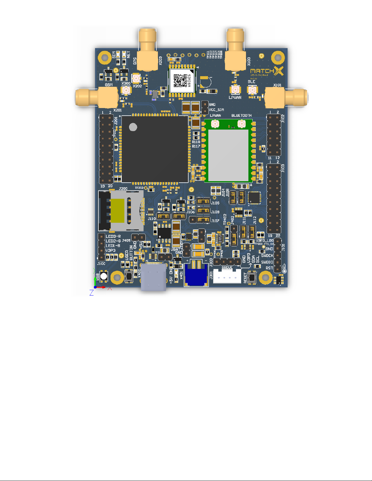
MatchX Dev Kit
LoRa Development Board with Grove Sensors
User Guide
Rev 1.0
Page 2

Copyrightc 2017 MatchX GmbH
WW W.MATC HX.I O
No part of the specifications may be reproduced in any form or by any means or used to make any
derivative such as translation, transformation, or adaptation without permission from MatchX GmbH
All rights reserved.
First release, Nov 2017
Page 3
Contents
1 Introduction . . . . . . . . . . . . . . . . . . . . . . . . . . . . . . . . . . . . . . . . . . . . . . . . . . . . 5
1.1 Product overview . . . . . . . . . . . . . . . . . . . . . . . . . . . . . . . . . . . . . . . . . . . . . . . . 5
1.1.1 Lora . . . . . . . . . . . . . . . . . . . . . . . . . . . . . . . . . . . . . . . . . . . . . . . . . . . . . . . . . . . . 5
1.1.2 BLE . . . . . . . . . . . . . . . . . . . . . . . . . . . . . . . . . . . . . . . . . . . . . . . . . . . . . . . . . . . . . 6
1.2 Main Features . . . . . . . . . . . . . . . . . . . . . . . . . . . . . . . . . . . . . . . . . . . . . . . . . . . 6
1.2.1 Hardware . . . . . . . . . . . . . . . . . . . . . . . . . . . . . . . . . . . . . . . . . . . . . . . . . . . . . . . . 6
1.2.2 Software . . . . . . . . . . . . . . . . . . . . . . . . . . . . . . . . . . . . . . . . . . . . . . . . . . . . . . . . . 6
2 Hardware Architecture - SoM module . . . . . . . . . . . . . . . . . . . . . . . . . . . . 7
2.1 Pin-out and pin description of the SoM module . . . . . . . . . . . . . . . . . . . . . . . 7
2.1.1 Dimensions . . . . . . . . . . . . . . . . . . . . . . . . . . . . . . . . . . . . . . . . . . . . . . . . . . . . . . . 9
2.2 Operating frequency bands . . . . . . . . . . . . . . . . . . . . . . . . . . . . . . . . . . . . . . 10
2.2.1 EU 863-870MHz ISM Band . . . . . . . . . . . . . . . . . . . . . . . . . . . . . . . . . . . . . . . . . . . 10
2.2.2 US 902-928MHz ISM Band . . . . . . . . . . . . . . . . . . . . . . . . . . . . . . . . . . . . . . . . . . . 10
2.2.3 Australia 915-928MHz ISM Band . . . . . . . . . . . . . . . . . . . . . . . . . . . . . . . . . . . . . . 10
3 Hardware Architecture - Evaluation Board . . . . . . . . . . . . . . . . . . . . . . 13
3.1 Block Diagram . . . . . . . . . . . . . . . . . . . . . . . . . . . . . . . . . . . . . . . . . . . . . . . . . . 13
3.2 Hardware features . . . . . . . . . . . . . . . . . . . . . . . . . . . . . . . . . . . . . . . . . . . . . . 15
3.3 Connectors . . . . . . . . . . . . . . . . . . . . . . . . . . . . . . . . . . . . . . . . . . . . . . . . . . . . 16
3.3.1 Connectors pin-out . . . . . . . . . . . . . . . . . . . . . . . . . . . . . . . . . . . . . . . . . . . . . . . 17
3.4 Jumpers and test connectors . . . . . . . . . . . . . . . . . . . . . . . . . . . . . . . . . . . . . 20
Page 4

4
3.5 Hardware selectable options . . . . . . . . . . . . . . . . . . . . . . . . . . . . . . . . . . . . . 21
4 Sensor connection . . . . . . . . . . . . . . . . . . . . . . . . . . . . . . . . . . . . . . . . . . . . . 23
4.1 Grove Digital . . . . . . . . . . . . . . . . . . . . . . . . . . . . . . . . . . . . . . . . . . . . . . . . . . . 23
4.2 Grove Analog . . . . . . . . . . . . . . . . . . . . . . . . . . . . . . . . . . . . . . . . . . . . . . . . . . 23
4.3 Grove UART . . . . . . . . . . . . . . . . . . . . . . . . . . . . . . . . . . . . . . . . . . . . . . . . . . . . 24
4.4 Grove I2C . . . . . . . . . . . . . . . . . . . . . . . . . . . . . . . . . . . . . . . . . . . . . . . . . . . . . . 24
5 Quick Installation Guide . . . . . . . . . . . . . . . . . . . . . . . . . . . . . . . . . . . . . . . 25
5.1 Software and Hardware requirements . . . . . . . . . . . . . . . . . . . . . . . . . . . . . . 25
5.2 Connections . . . . . . . . . . . . . . . . . . . . . . . . . . . . . . . . . . . . . . . . . . . . . . . . . . . 25
5.2.1 Power . . . . . . . . . . . . . . . . . . . . . . . . . . . . . . . . . . . . . . . . . . . . . . . . . . . . . . . . . . 25
5.2.2 Bluetooth connection . . . . . . . . . . . . . . . . . . . . . . . . . . . . . . . . . . . . . . . . . . . . . 26
5.3 Setup . . . . . . . . . . . . . . . . . . . . . . . . . . . . . . . . . . . . . . . . . . . . . . . . . . . . . . . . . . 26
5.4 Registering a node on MarchX server . . . . . . . . . . . . . . . . . . . . . . . . . . . . . . 26
5.5 Setting DevEUI, AppEUI and DevKey . . . . . . . . . . . . . . . . . . . . . . . . . . . . . . . 27
5.6 Region Selection . . . . . . . . . . . . . . . . . . . . . . . . . . . . . . . . . . . . . . . . . . . . . . . . 28
6 Software Development Guide . . . . . . . . . . . . . . . . . . . . . . . . . . . . . . . . . . 30
6.1 References . . . . . . . . . . . . . . . . . . . . . . . . . . . . . . . . . . . . . . . . . . . . . . . . . . . . . 30
6.2 Prerequisites . . . . . . . . . . . . . . . . . . . . . . . . . . . . . . . . . . . . . . . . . . . . . . . . . . . . 30
6.3 Software development under Windows OS . . . . . . . . . . . . . . . . . . . . . . . . . . 31
6.3.1 Using SmartSnippet Studio . . . . . . . . . . . . . . . . . . . . . . . . . . . . . . . . . . . . . . . . . . 33
6.4 Software development under Linux . . . . . . . . . . . . . . . . . . . . . . . . . . . . . . . . 36
7 Product specification . . . . . . . . . . . . . . . . . . . . . . . . . . . . . . . . . . . . . . . . . . 37
7.1 Software environment . . . . . . . . . . . . . . . . . . . . . . . . . . . . . . . . . . . . . . . . . . . 37
7.2 Hardware environment . . . . . . . . . . . . . . . . . . . . . . . . . . . . . . . . . . . . . . . . . . 37
7.2.1 RF performance . . . . . . . . . . . . . . . . . . . . . . . . . . . . . . . . . . . . . . . . . . . . . . . . . . 38
7.2.2 Electrical characteristics . . . . . . . . . . . . . . . . . . . . . . . . . . . . . . . . . . . . . . . . . . . 38
7.2.3 Antenna characteristics . . . . . . . . . . . . . . . . . . . . . . . . . . . . . . . . . . . . . . . . . . . 39
7.3 Dimensions . . . . . . . . . . . . . . . . . . . . . . . . . . . . . . . . . . . . . . . . . . . . . . . . . . . . . 40
7.4 Certification . . . . . . . . . . . . . . . . . . . . . . . . . . . . . . . . . . . . . . . . . . . . . . . . . . . . 41
Page 5
1. Introduction
1.1 Product overview
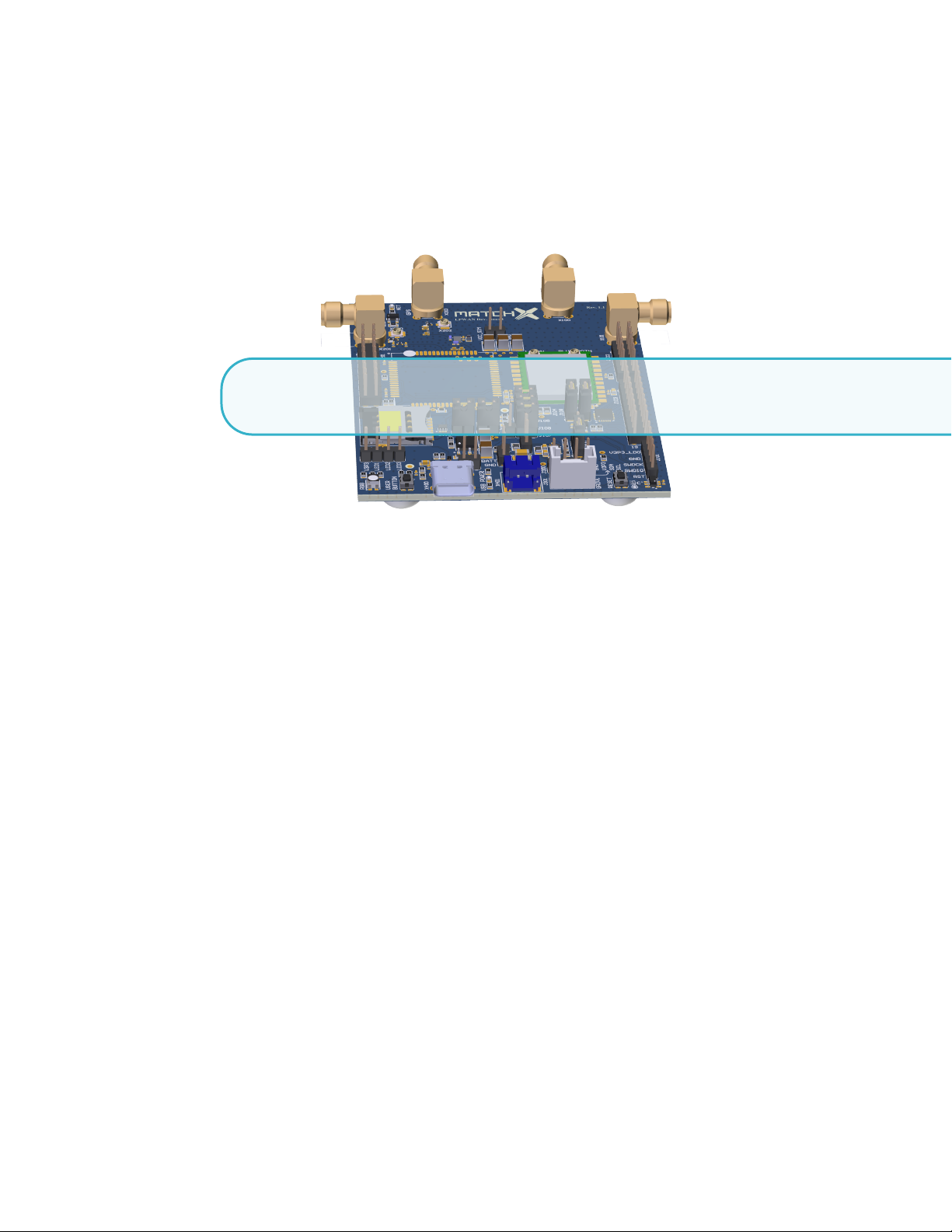
The LPWAN Dev Kit by MatchX is a high performance, ready to use development platform allowing
you to kick-start your IoT project. Together with a MatchX Core module the Dev Kit is an incredibly
flexible solution that can be deployed in a various number of applications which require long distance
communication and long battery life. The unique combination of both LoRa and Bluetooth Low
Energy makes non-contact firmware updates easy, especially when the device is mounted in a
unaccessible place.
This guide covers both the US and EU version of the Dev Kit. The main differences between
these two versions are listed in Table 1.1.number
Parameter US EU
Operating Frequency Band 902-928MHz 863-870MHz
Maximum Output Power +17dBm +14dBm
Lora BW 500k/125kHz 125kHz
SF 7-10 7-12
Certification IEC 60950-1 EN 300200
FCC PART 15.247 EN 301489
1.1.1 Lora
The MatchX Module uses LoRa communication to send messages over long distances (up to 20km
in open spaces). This unique modulation scheme guarantees robust wireless communication even in
difficult from RF point of view environments such as high-rise city landscapes or within the inside
of buildings. The module can output up to 17dBm of power and is fully LoraWAN compatible. It’s
uniquely designed to work with the MatchX Box gateway and can also be used with a LoraWAN
Table 1.1: Comparison of different regions
Page 6

6 Chapter 1. Introduction
compatible Gateway of your choice.
1.1.2 BLE
The module offers a novel firmware solution upgrade by augmenting LoRa, together with Bluetooth
Low Energy (BLE). As LoRa protocol is not suitable for transmitting large amounts of data, MatchX
has combated this with BLE, offering a quick, robust and remote way of updating your software.
It is a perfect method in cases where a sensor may be mounted in an unaccessible place like in a
basement, sealed container box or behind a wall. Moreover BLE together with provided mobile app
enables you to configure your module and read its status and additional data.
1.2 Main Features
LPWAN Dev Kits long range, long battery life, flexible sensor configuration and wireless firmware
update are the key features that are offered by the Core module.
1.2.1 Hardware
• integrated MatchX Core System on Module
• +18.5dBm output power in 868MHz/915MHz
• -146dBm sensitivity of LoraWAN packets
• integrated Semtech SX1276 LoRa and Bluetooth Low Energy
• 0 Hz up to 96 MHz 32-bit ARM Cortex-M0 Dialog DA14680 microcontroller
• GPS receiver with 22 tracking / 66 acquisition- channels
• optional NB-IOT, Tri-Band LTE-FDD and Dual-Band GPRS/EDGE module
• integrated Li-ION battery charger
• 16 bit I/O expander
• GROVE sensor connector
• RGB indicator LED and User Button
• temperature sensor with 0.125◦C resolution and 1◦C accuracy
• unique ID EEPROM memory
• ultra low power design
1.2.2 Software
• Runs LoRa and Bluetooth stack simultaneously
• Low power consumption modes
• Easy to use software package
• Eclipse-based IDE
• Firmware upgrade over the air
• Mobile application
Currently there is no Class B support in server yet, but the hardware and firmware are fully
R
prepared for Class B specification, it is expected to support Class B in future firmware upgrade.
Page 7
2. Hardware Architecture - SoM module
2.1 Pin-out and pin description of the SoM module
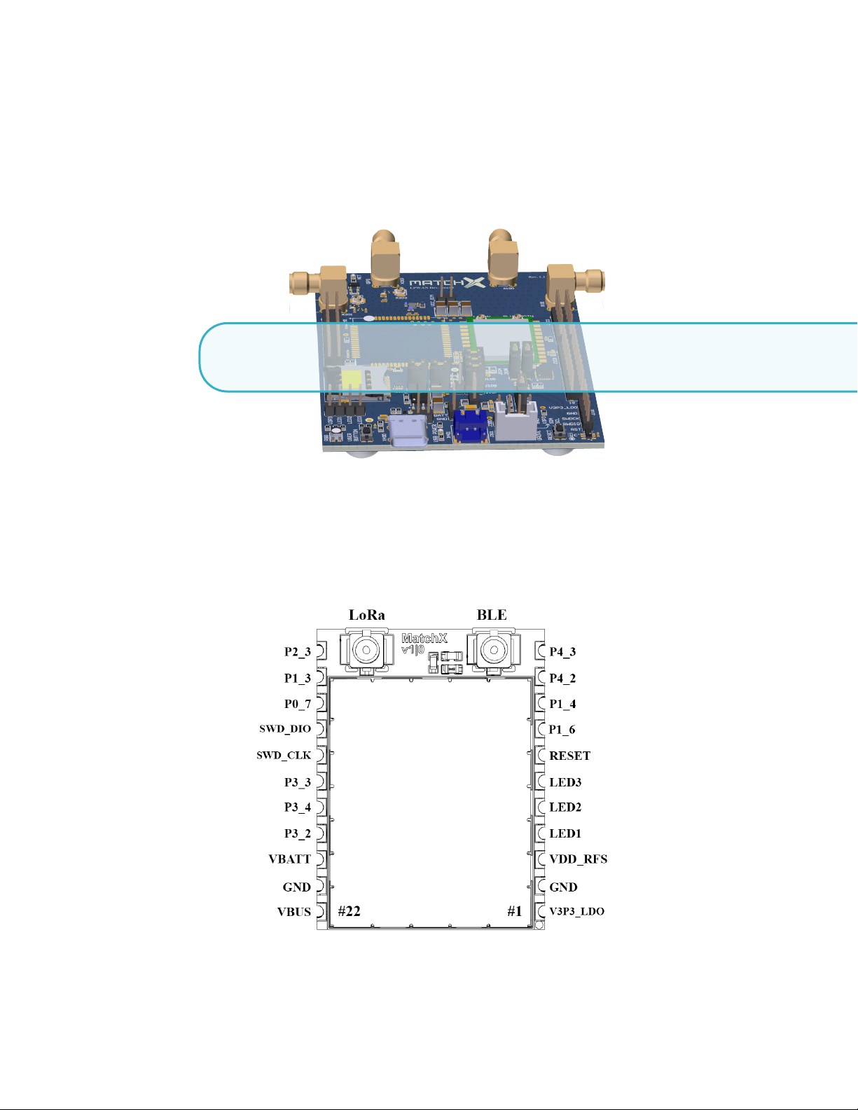
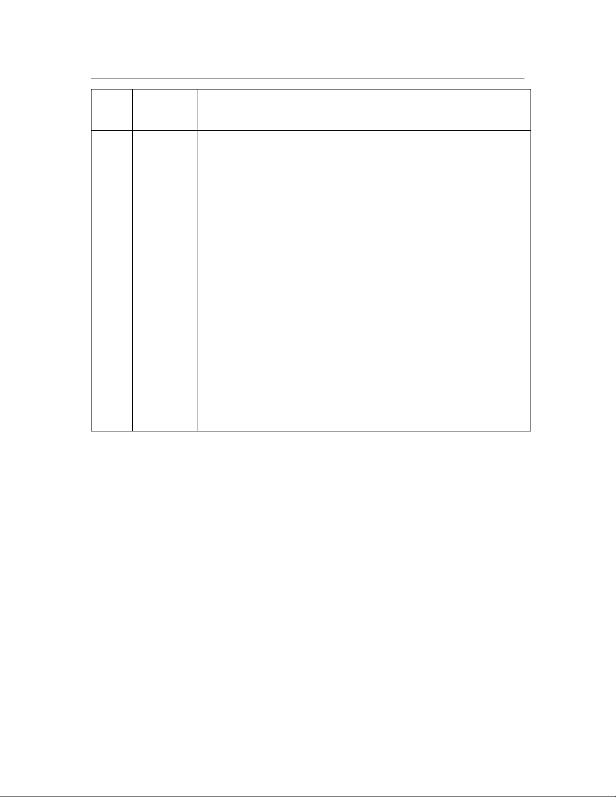
The pin-out of the MatchX Core SoM module can be seen on Figure 2.1 and the description of the
pins in Table 2.1. On top of the module there are two UF.L RF connectors, the one on the left is the
LoRa antenna connector, a suitable 868MHz in EU and 915MHz in US, 50 Ohm antenna is expected
to be connected on these port. The other connector is for connecting the 2.4GHz, 50 Ohm BLE
antenna. Both antennas come together with the evaluation board.
Figure 2.1: Pin-out of the SoM module.
Page 8
8 Chapter 2. Hardware Architecture - SoM module
Pin
number
1
2
3
4
5
6
7
8
9
10
11
12
13
14
15
16
17
18
19
20
21
22
Name Description
V3P3_LDO 3.3V output of the internal LDO
GND Ground
VDD_RFS Supply voltage of the radio front-end
LED1 Open drain output type, LED driver
LED2 Open drain output type, LED driver
LED3 Open drain output type, LED driver
RESET Reset signal, active high
P1_6 General Purpose I/O P1_6 / NTC resistor for battery temperature sensing
P1_4 General Purpose I/O P1_4 / ADC1 / battery temperature sensing
P4_2 General Purpose I/O P4_2
P4_3 General Purpose I/O P4_3
P2_3 General Purpose I/O P2_3
P1_3 General Purpose I/O P1_3 / ADC2
P0_7 General Purpose I/O P0_7 / ADC3
SWD_DIO Serial Wire Debug interface I/O signal / GPIO P0_6 / ADC4
SWD_CLK Serial Wire Debug interface clock signal / GPIO P2_4 / ADC7
P3_3 General Purpose I/O P3_3
P3_4 General Purpose I/O P3_4
P3_2 General Purpose I/O P3_2
VBATT Battery voltage input
GND Ground
VBUS 5V supply, charging voltage
Table 2.1: USB-C connector pins description.
The module can be powered in two ways:
1. By connecting the VBATT to a battery voltage (2.7V to 4.2V).
2. By supplying +5V on the VBUS pin.
If both power sources are present, the battery will be charged form +5V power supply. The charging
current and charging characteristics for different battery types is software configurable. The module
provides
used to supply external devices, but the maximum current drawn can’t be grater than 100mA. By
default
VDD_RFS
with +17dBm power. This has to be taken in consideration when planning the power budget of
V3P3_LDO
power source for
low power converter.
LDO, when
battery voltage. By default all GPIO are referenced to
1.8V as the GPIO level, each GPIO can be configured individually) so care must be taken to ensure
V3P3_LDO
VDD_RFS
is around 35mA during transmission with +14dBm power output and around 90mA
. When even higher RF transmission power is required it is advisable to use different
The source of
VBUS
voltage, it is a output of internal LDO of the DA14680 MCU, and it can be
is connected to
VDD_RFS
V3P3_LDOisVBUS
is not present, and
V3P3_LDO
. On the Evaluation Board it can be done by using 3.3V output of the
when present or
VBATT
with an external 0R resistor. The current draw of
VBATT
drops below 3.3V the
V3P3_LDO
otherwise. As it is a output of a
V3P3_LDO
(it is also possible to configure
will follow the
Page 9
2.1 Pin-out and pin description of the SoM module 9
that no voltage higher than
external devices, that connect to SoM module, from a boost converter.
V3P3_LDO
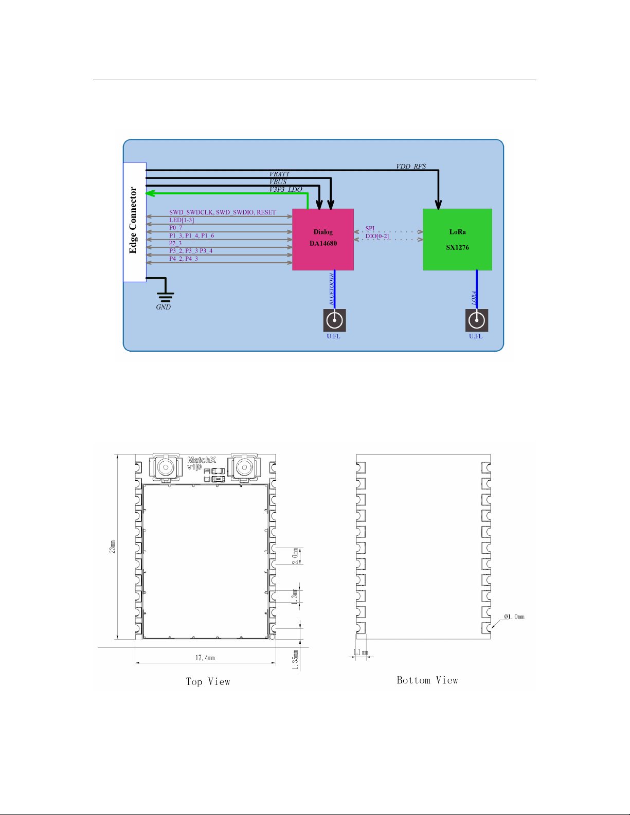
Figure 2.2: Block diagram of the Core module.
is presented to any GPIO. This may happen when powering
2.1.1 Dimensions
Figure 2.3: Dimension of the SoM module.
Page 10
10 Chapter 2. Hardware Architecture - SoM module
2.2 Operating frequency bands
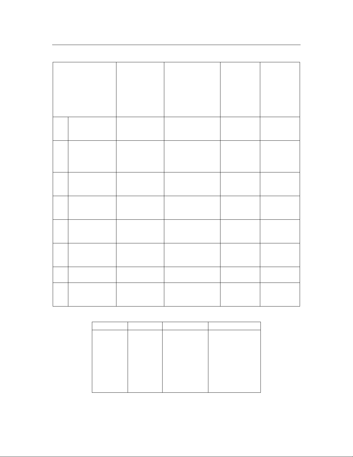
2.2.1 EU 863-870MHz ISM Band
In the European region the EN300220-2 V3.1.1 (2017-02) regulation defines the allowed frequency
allocation and spectrum access. Every device working in this band must comply with these rules
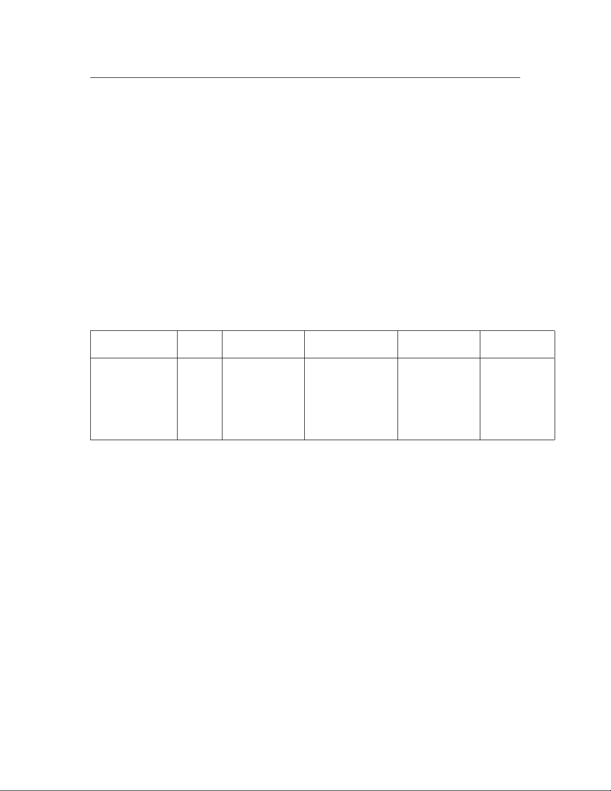
as shown in the Table 2.3. EU regulations restrict the maximum radiated power as well as the duty
cycle of the transmission in different frequency bands.To comply with the duty cycle requirement the
transmitting device must wait after every transmitted packet. The time device has to wait depends
on the time on air of transmitted packet and this in turn depends on the length of the packet and
spreading factor SF. This relation and required wait time can be seed in Table 2.2 According to
LoRaWAN specification every device has to implement at least 3 channels as follows:
• 868.10 MHz
• 868.30 MHz
• 868.50 MHz
The SoM is preconfigured to work with the MatchX Box gateway and additionally to the 3 mandatory
channels 5 additional channels are defined. The list of all preconfigured channels can be found in
Table 2.4.
Spreading Factor Bit rate Range (depends Time on air (ms) 0.1% duty cycle 1% duty cycle
(125kHz Lora) (bps) on conditions) (10 bytes payload) waiting time waiting time
SF7 5470 2 km 56 ms 1 min 6s
SF8 3125 4 km 100 ms 1 min 40s 10s
SF9 1760 6 km 200 ms 3 min 20s 20s
SF10 980 8 km 370 ms 6 min 10s 37s
SF11 440 14 km 740 ms 12 min 20s 1 min 14s
SF12 290 20 km 1400 ms 23 min 20s 2min 20s
Table 2.2: Modules operating frequencies.
2.2.2 US 902-928MHz ISM Band
These frequencies band can be used in USA, Canada and all other countries that adopt the entire
FCC-Part15 regulations in 902-928 ISM band. For these region MatchX uses predefined frequencies
listed in Table 2.5. The FCC regulation puts restriction on the maximum dwell time of 400ms in
uplink, thats why the maximum allowed spreading factor is SF10.
2.2.3 Australia 915-928MHz ISM Band
These frequencies band can be used in Australia region. For these region MatchX uses predefined
frequencies listed in Table 2.6. All channels use 125kHz bandwidth and maximum of +20dBm
output power can be reached.
Page 11
2.2 Operating frequency bands 11
Class 1 sub-
Operational Frequency band
863,000 MHz to
K
865,000 MHz
865,000 MHz to
L
868,000 MHz
868,000 MHz to
M
868,600 MHz
868,700 MHz to
N
869,200 MHz
869,400 MHz to
O
869,650 MHz
869,400 MHz to
P
869,650 MHz
869,700 MHz to
Q
870,000 MHz
869,700 MHz to
R
870,000 MHz
Channel access and
Maximum e.r.p
25 mW e.r.p.
25 mW e.r.p.
Power density:
-4,5 dBm/100
kHz
25 mW e.r.p.
25 mW e.r.p.
25 mW e.r.p.
500 mW e.r.p.
5 mW e.r.p. No requirement 56a 31
25 mW e.r.p.
occupation rules
(e.g. Duty cycle or
LBT + AFA)
≤
0,1% duty cycle
or polite spectrum
access
≤
1 % duty cycle or
polite spectrum access
≤
1% duty cycle or
polite spectrum access
≤
0,1% duty cycle
or polite spectrum
access
≤
0,1% duty cycle
or polite spectrum
access
≤
10 % duty cycle
or polite spectrum
access
≤
1% duty cycle or
polite spectrum access
Band number from
EC Decision
2013/752/EU
[i.3]
46a 66
47 67
48 28
50 29
54a 130
54b 30
56c 69
class number
according
Commission
Decision
2000/299/EU
[i.7]
Table 2.3: EU wide harmonized national radio interfaces.
Frequency Bandwidth Maximum e.r.p Channel access
864.7 MHz 125 kHz 14 dBm ≤0,1% duty cycle
864.9 MHz 125 kHz 14 dBm ≤0,1% duty cycle
865.1 MHz 125 kHz -4.5 dBm ≤1% duty cycle
865.3 MHz 125 kHz -4.5 dBm ≤1% duty cycle
868.1 MHz 125 kHz 14 dBm ≤1% duty cycle
868.3 MHz 125 kHz 14 dBm ≤1% duty cycle
868.5 MHz 125 kHz 14 dBm ≤1% duty cycle
868.8 MHz 125 kHz 14 dBm ≤0,1% duty cycle
Table 2.4: Core Module operating frequencies in EU 863-870MHz ISM Band.
Page 12
12 Chapter 2. Hardware Architecture - SoM module
Channel number Frequency Channel number Frequency
1 903.90 MHz 5 904.70 MHz
2 904.10 MHz 6 904.90 MHz
3 904.30 MHz 7 905.10 MHz
4 904.50 MHz 8 905.30 MHz
Table 2.5: Modules operating frequencies (uplink) in US 902-928MHz ISM Band.
Channel number Frequency Channel number Frequency
1 915.20 MHz 5 916.00 MHz
2 915.40 MHz 6 916.20 MHz
3 915.60 MHz 7 916.40 MHz
4 915.80 MHz 8 916.60 MHz
Table 2.6: Modules operating frequencies (uplink) in Australia 915-928MHz ISM Band.
Page 13
3. Hardware Architecture - Evaluation Board
3.1 Block Diagram
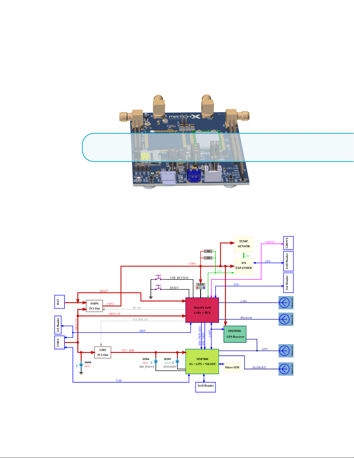
The development board comprises of two main subsystems:
1. MatchX SoM with LoRa and Bluetooth radios
2. SIMCom SIM7000E NB-IOT module with 3G/4G and GPS
Figure 3.1: Block diagram of the Dev Kit.
Page 14

14 Chapter 3. Hardware Architecture - Evaluation Board
MatchX SoM is the core of the Dev Kit. It is responsible for controlling the SIMCom module,
accessing the sensors, I/O expender, RGB LED etc. It also controls different power rails enabling
low power modes.
The Dev Kit can be powered by USB-C +5V and/or Lithium-ion battery connected to X401
connector.The presence of +5V is signaled by a red LED next to USB-C. When both +5V and battery
are present the MatchX SoM will start to charge the battery. The battery type, charging current, and
charging curve are software configurable.
MatchX SoM provides
capable to deliver up to 100mA of current. As it is used to power the LoRa RF front-ent by default,
it can be used to power just very low power peripherals. If more current is needed, a onboard SMPS
TPS62740 should be used. It outputs a 3.3V up to 300mA current. Its output should be connected to
the V3P3 power rail with the J402 jumper in position 1-2.
The SIMCom module is optional and is not included in a standard package but all peripheral
components are already soldered. The main communication interface between MatchX SoM and
SIMCom module is UART together with two control lines (SIM_NRST and SIM_PWR_KEY).
Please refer to SIMCom SIM7000E datasheet to find more information about the modules operation.
The SIM7000E is powered from +5V provided by USB-C connector which is converted to 3.3V by a
LDO. Its enable pin can be controlled by a SoM or can be always set high by a jumper.
The Dev Kit offers two ways to receive GPS signal. One is by using aforementioned SIM7000E
module. A cheaper and less power demanding alternative is using SIM28ML.
V3P3_LDO
output, which is a low current output of internal LDO
Page 15
3.2 Hardware features 15
3.2 Hardware features
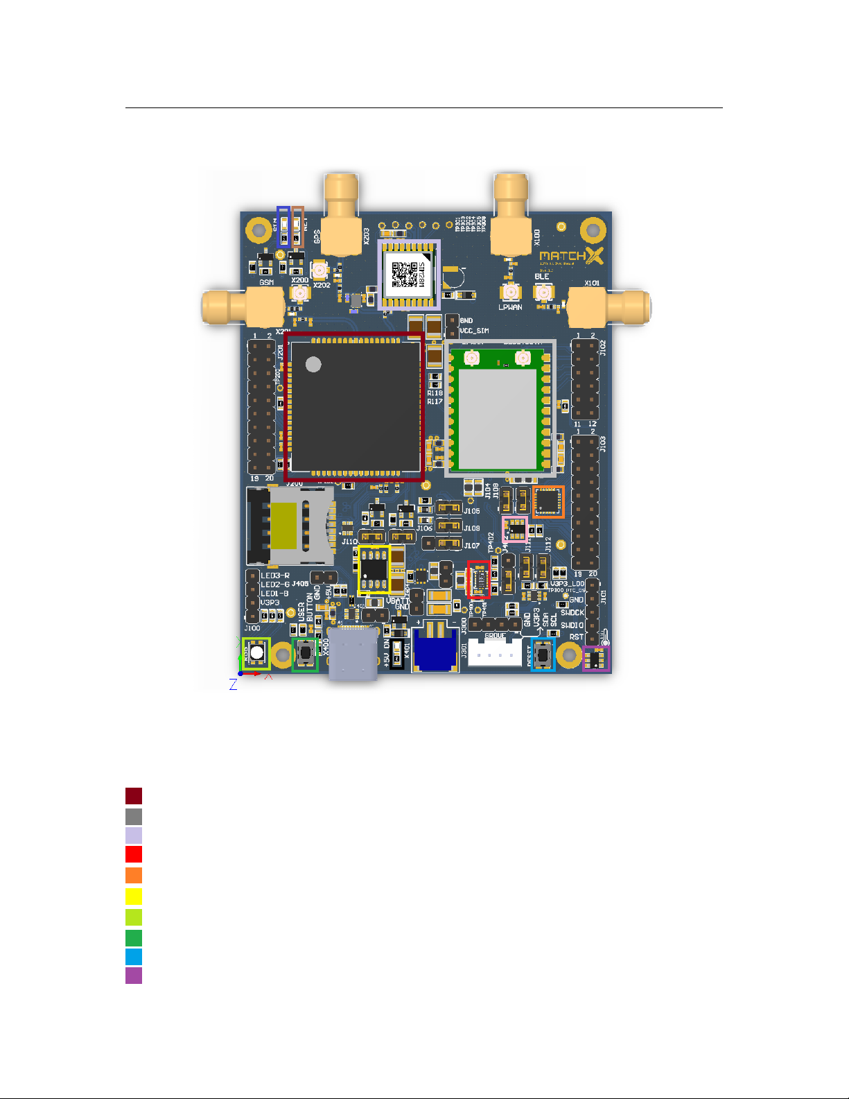
Figure 3.2: Hardware features of the Dev Kit.
Components marked on the Figure 3.2 are:
Optional SIMCOM SIM7000E NB-IOT module with 3G/4G and GPS
MatchX SoM module with LoRa and Bluetooth
SIM28ML GPS receiver
3.3V low power converter for sensors supply
PCA6416A I2C I/O expander
3.3V LDO for powering the optional SIM7000E module
RGB LED controlled by the MatchX SoM
User button, connected to P3_2 of the SoM module
Reset button for MatchX SoM
PCT2075GV I2C temperature sensor
Page 16
16 Chapter 3. Hardware Architecture - Evaluation Board
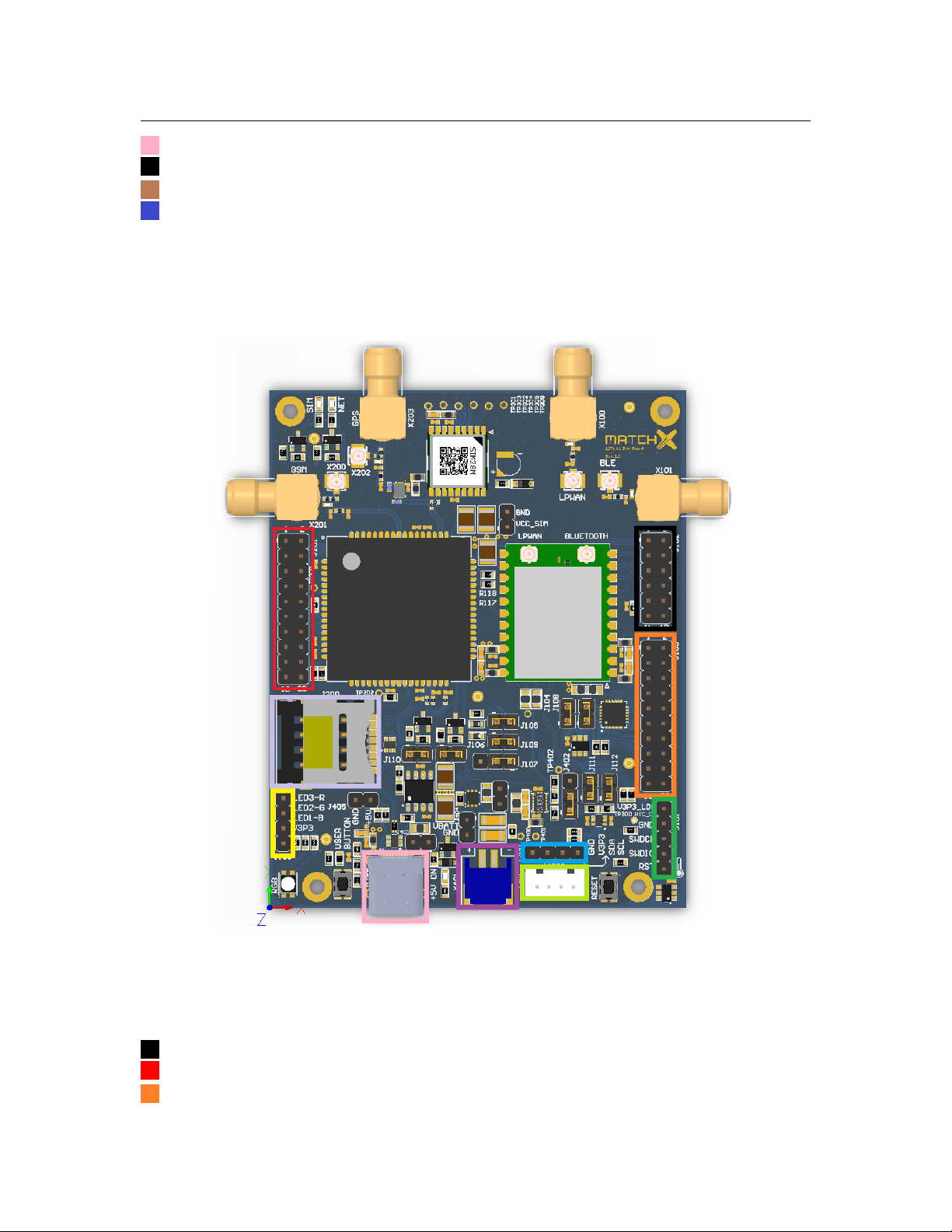
I2C Serial EEPROM 24AA025UIDT-I/OT
LED indicating presence of USB +5V
NET indication LED of the SIM7000E
LED indicating presence of SIM card
3.3 Connectors
Figure 3.3: Connectors on the Dev Kit.
Connectors marked on the Figure 3.3 are:
J102 MatchX SoM modules I/Os
J201 SIM7000E I/Os and signals
J103 PCA6416A I/Os
Page 17
3.3 Connectors 17
J100 RGB LED control signals
J301 Grove sensors I2C connector
J101 MatchX SoM SWD programming and debugging connector
J300 I2C connector
X401 S2B-PH-SM4-TB Lithium battery connector
USB-C connector, +5V supply and programming
SIM card socket for SIM7000E
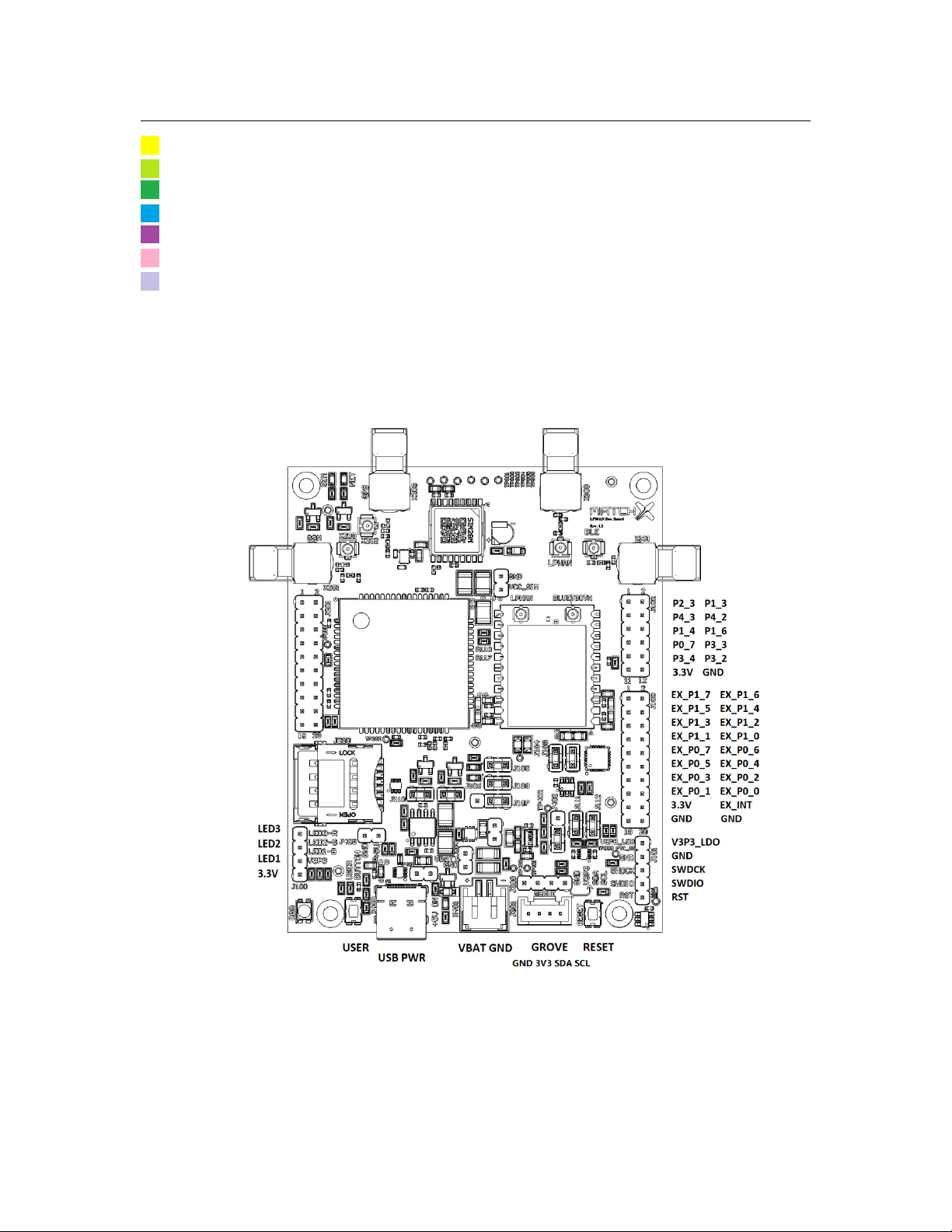
3.3.1 Connectors pin-out
Figure 3.4: Pin-out of the Dev Kit.
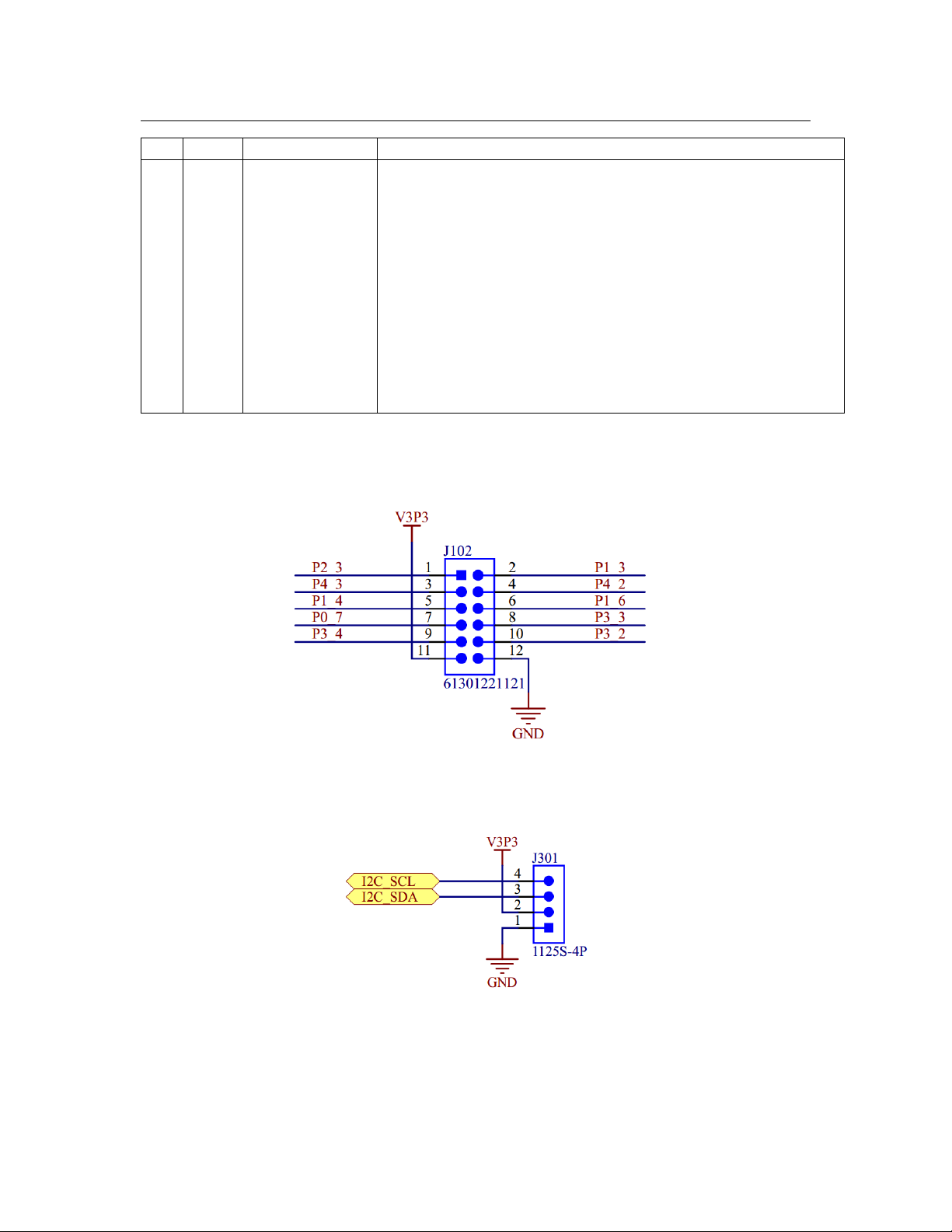
The J102 connector, shown on Figure 3.5 routs out all GPIOs available on the MatchX SoM
module. Some of these GPIOs are used by default to control functions of the Dev Kit.
Page 18
18 Chapter 3. Hardware Architecture - Evaluation Board
Pin Name Function Description
1 P2_3 UART_SIM_RX UART interface to SIMCom module, connected with J109 jumper
2 P1_3 UART_SIM_TX UART interface to SIMCom module, connected with J105 jumper
3 P4_3 I2C_SCL Main I2C bus, connected with J104 jumper
4 P4_2 I2C_SDA Main I2C bus, connected with J108 jumper
5 P1_4 - Not used
6 P1_6 - Not used
7 P0_7 - Not used
8 P3_3 - Not used
9 P3_4 PS_EN controls enable pin of TPS62740
10 P3_2 USR_BUTTON User button connection
11 V3P3 3.3V 3.3V power, the source selectable by J402 jumper
12 GND GND Ground
Table 3.1: Functions assignment of the MatchX SoM GPIOs
Figure 3.5: Pin-out of J102 connector.
Figure 3.6: Pin-out of J301 connector.
Page 19
3.3 Connectors 19
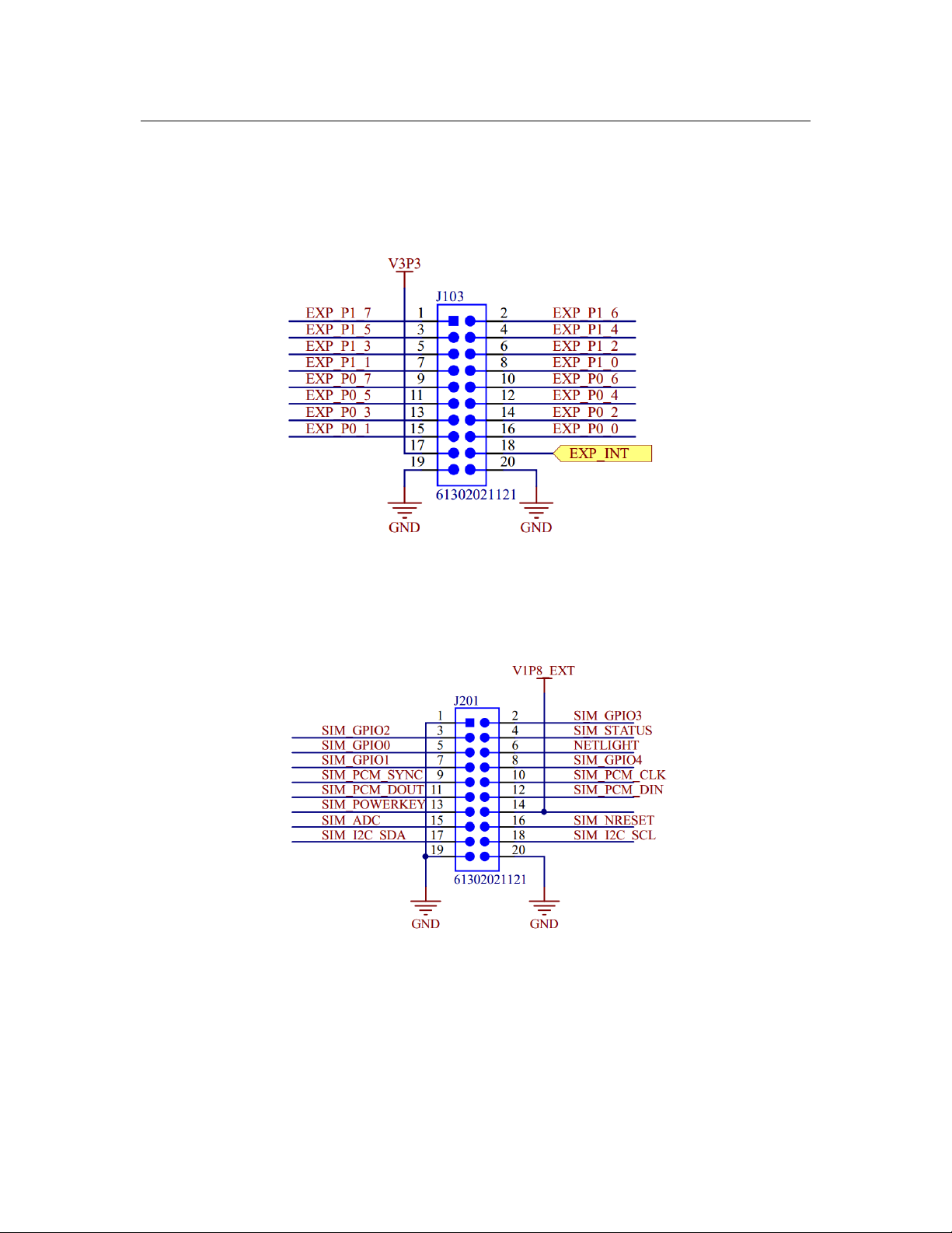
The J103 connector, shown on Figure 3.7, exposes all pins available on the PCA6416A I2C I/O
expander. It offers 16 I/Os organized in two ports P0 and P1. Each pin can be configured individually
as a input or output, and its state can be read and set by the I2C commands. Additionally there is a
interrupt line EXP_INT that is being driven by the PCA6416A when input IO changes it state.
Figure 3.7: Pin-out of J103 connector.
The J201 connector, depicted on Figure 3.8, exposes all unused pins of the SIMCom SIM7000E
module. For more information about the signals functions please refer to the modules datasheet.
Figure 3.8: Pin-out of J201 connector.
Page 20
20 Chapter 3. Hardware Architecture - Evaluation Board
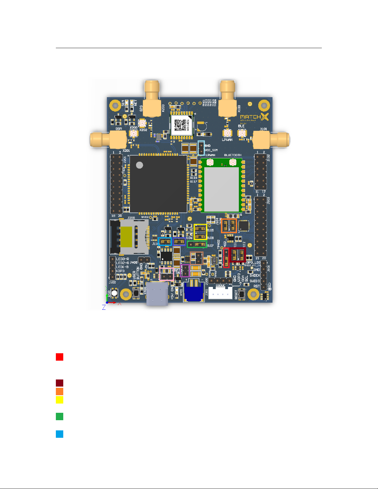
3.4 Jumpers and test connectors
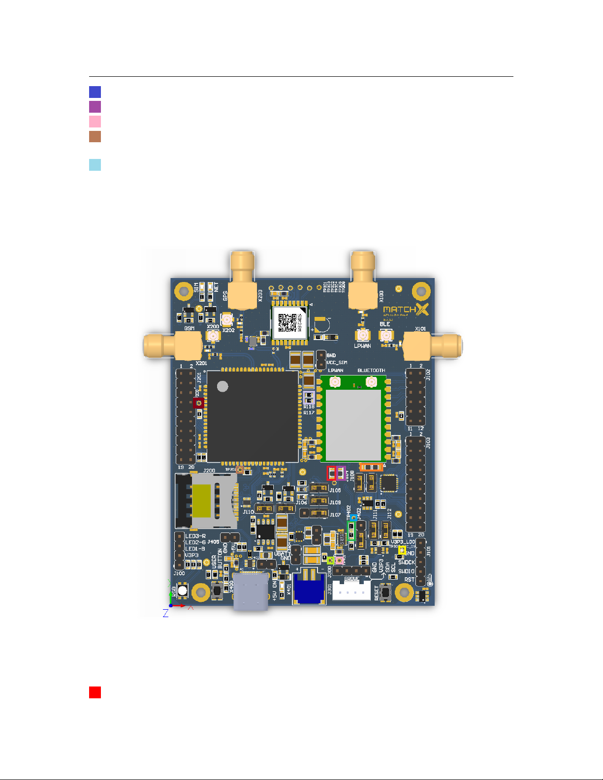
Figure 3.9: Jumpers and test connectors on the Dev Kit.
Components marked on the Figure 3.9 are:
J402 - selection of the source of V3P3 used to power RGB LED and sensors. A jumper
in position 1-2 selects the 3V3 from low power converter (located left), jumper in position 2-3
selects the V3P3_LDO output from integrated LDO of the SoM module
J111, J112 - connect the P1_3 and P0_7 to Grove D1 and D2 lines
J104, J108 - connect the P4_2 and P4_3 to I2C_SDA and I2C_SCL
J105, J109 - connect P1_2 and P2_3 of MatchX SoM to UART_SIM_TX and UART_SIM_RX
of the SIM7000E module
J107 - connects the enable line of the 3.3V LDO that powers SIM7000E ether to EXT_P0_2
(I/O expander) in position 1-2 or to 5V (always on) in position 2-3.
J110 - connects SIM_NRST of the SIM7000E to EXT_P0_1 of the I/O expander
Page 21
3.5 Hardware selectable options 21
J106 - cconnects SIM_PWR_KEY of the SIM7000E to EXT_P0_0 of the I/O expander
J404 - test connector of the battery voltage
J401 - connects USB +5V to the input of the LDO, it is bypassed by a 0R resistor by default
J403 - connects power to the input of the low power 3.3V converter, the source of the power is
USB +5V or battery if the +5V is not present.
J400 - test connector of the VCC_SIM (by default it is a 3.3V output of the LDO)
3.5 Hardware selectable options
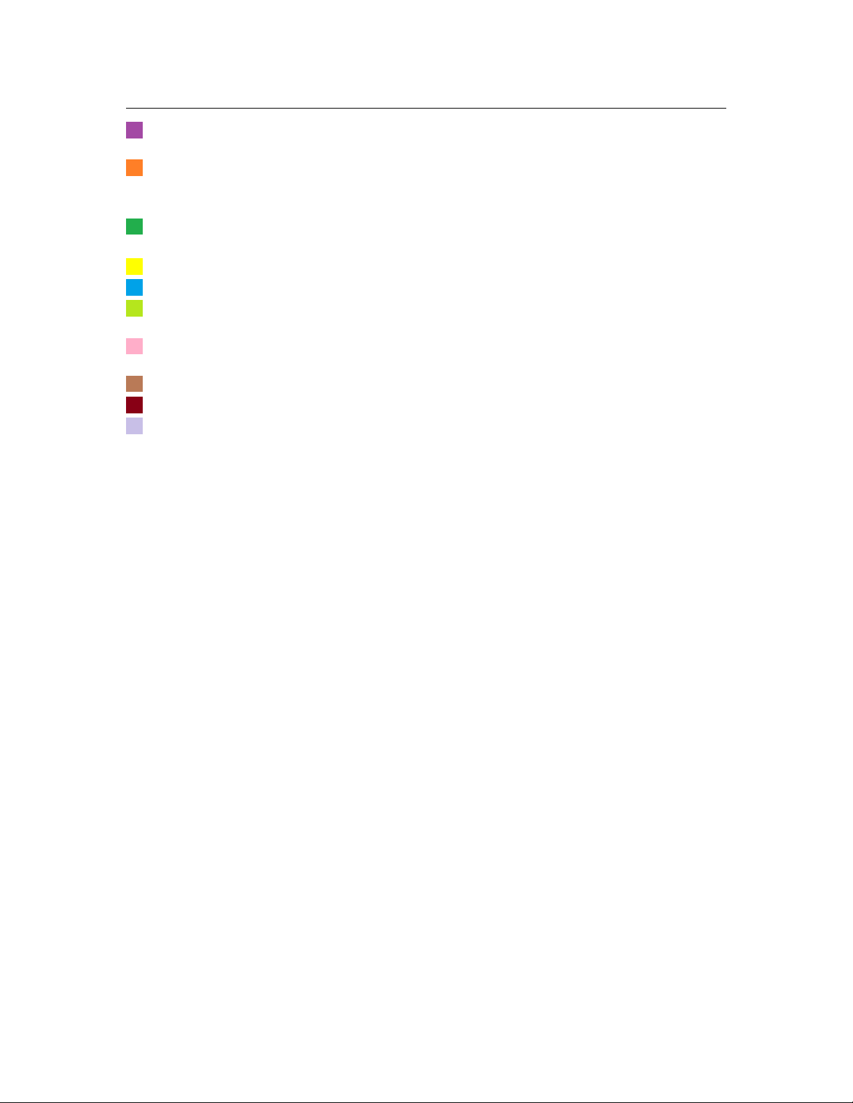
Figure 3.10: Hardware options of the Dev Kit.
Components marked on the Figure 3.10 are:
0R jumper connects P3_2 of SoM module to the User Button
Page 22
22 Chapter 3. Hardware Architecture - Evaluation Board
0R jumper connects P3_4 of SoM module to PS_EN, a enable signal of the low power 3.3V
converter
0R jumper selectin the source of VDD_RFS (the radio frontend power). The 0R connected on
the left side connects the VDD_RFS to low power 3.3V converter, jumper soldered on the right
side connects VDD_RFS to the V3P3_LDO (the output of internal LDO of the SoM)
2.2M Ohm resistor connected in the upper position pulls the enable line of the low power 3.3V
converter low, in the lower position pulls this line up
test point connected to the interrupt line of the temperature sensor (PTC_OS)
test point connected to the power good pin of low power 3.3V converter
test point connected to the CNTRL pin of low power 3.3V converter, pulling it high enables the
internal LDO
test point connected to the LOAD pin of low power 3.3V converter, it is a output of internal
LDO
test point connected to the SIM_MDM_LOG pin of the SIM7000E module
test point connected to the SIM_BOOT_CFG pin of the SIM7000E module
0R jumpers connect P2_3 and P3_3 GPS_UART_RXD and GPS_UART_TXD, they need to be
removed when SIM7000 is to be used
Page 23
4. Sensor connection
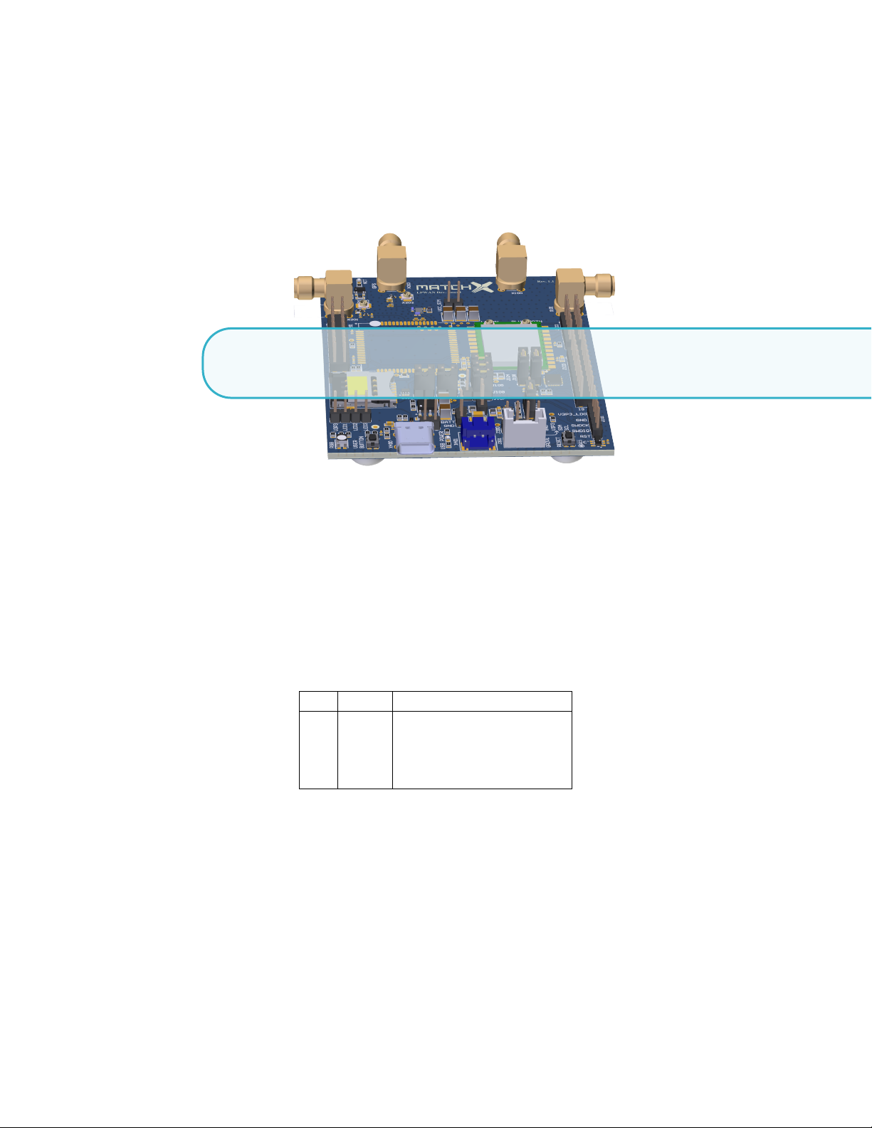
The Dev Kit is specifically designed to work with all different sorts of sensors, which can be attached
to its GROVE connector or to 2.54mm pin headers. This makes it a very flexible solution that can be
adjusted to specific applications and individual needs.
4.1 Grove Digital
The Grove digital modules use two signal lines called D0 and D1 . There are, for example, switch
Modules, the Fan Module, and the LED Module that controlled by digital GPIOs D0 and D1.
The following table shows the pin out of the Grove digital connector:
Pin Name Function
1 D0 Primary Digital I/0
2 D1 Secondary Digital I/0
3 VCC Power for Grove module
4 GND Ground for Grove module
Table 4.1: Pin-out of the Grove digital connector
4.2 Grove Analog
The Grove Analog modules use two signal lines called A0 and A1 . There are, for example,
Potentiometer, Voltage Divider, and the Air Quality Module that controlled by analog pins A0 and
A1.
The following table 4.2 shows the pin out of the Grove Analog connector:
Page 24
24 Chapter 4. Sensor connection
Pin Name Function
1 A0 Primary analog I/0
2 A1 Secondary analog I/0
3 VCC Power for Grove module
4 GND Ground for Grove module
Table 4.2: Pin-out of the Grove analog connector
4.3 Grove UART
The Grove UART modules use two signal lines RX and TX. There are, for example, RFID module
that controlled by UART pins TX and RX.
The following table 4.3 shows the pin out of the Grove UART connector:
Pin Name Function
1 RX Serial receive
2 TX Serial transmit
3 VCC Power for Grove module
4 GND Ground for Grove module
Table 4.3: Pin-out of the Grove UART connector
4.4 Grove I2C
The Grove I2C modules use two signal lines SDA and SCL. There are, for example, motion detect
module and environment module that controlled by I2C pins SDA and SCL.
The following table 4.4 shows the pin out of the Grove I2C connector:
Pin Name Function
1 SCL I2C Clock
2 SDA I2C data
3 VCC Power for Grove module
4 GND Ground for Grove module
Table 4.4: Pin-out of the Grove UART connector
Page 25
5. Quick Installation Guide
The Core module incorporated in the Dev Kit is by default configured to connect with MatchX
LoraWAN cloud server if the network coverage is present. Nonetheless some settings can be changed
and some set up may be required in order to use the Dev Kit in a custom application. This installation
guide will introduce how to set up the LoRa parameters and establish LoraWAN network connection.
5.1 Software and Hardware requirements
To configure the board, users will need to have the following:
• Dev Kit with USB-C power cable or Li-ion battery
• MatchX server account
• LoraWAN coverage by e.g. MatchX Box gateway
• USB-to-UART converter
• PC computer with Windows or Linux OS
5.2 Connections
5.2.1 Power
The Dev Kit is equipped with battery connector. As long as the battery is charged there is no other
connection required for the Dev Kit to work. Charging: If the LED is signaling that the battery needs
to be charged or the state of charge readouts from the mobile app or through LoRa are indicating low
battery it can be charged two ways:
1.
2.
By connecting the Dev Kit to a USB charger. A standard USB charger with 5V output and
minimum 500mA of current can be used and standard, reversible USB-C cable. The integrated
charging controller will take care of proper charging of the battery. This process can take up
to 12h.
By using a dedicated lithium battery charger . Using this method may result in a faster charging
process due to higher charging current. Please refer to the battery datasheet for details about
the charging characteristics.
Page 26
26 Chapter 5. Quick Installation Guide
Important!
!
MatchX strongly recommends to charge the battery within specified temperature range of 0 to
+45◦C. Charging outside of these reommended conditions may lead to either reduced battery
life or permanent damage.
5.2.2 Bluetooth connection
The Core module implements Bluetooth Low Energy (Bluetooth 4.2 specification) with SUOTA
(Software Update Over The Air) feature. The only hardware requirement is a connection of 2,4GHz,
50 Ohm antenna to BLE antenna port.
5.3 Setup
Every Dev Kit and Core module comes with preprogrammed unique MAC address, AppEUI and
LoraWAN DevKey (also referred as AppKey by different sources). The DevKey is used to ensure a
secure communication and data encryption between the module and application server. AppEUI is
used to communicate with the application that registered on the Lora server. Care must be taken
with storing the DevKey in a safe place and ensuring it is not compromised.
The products will come with a QR code sticker, which gives the Serial Number of the device. By
typing in the S/N at the registration of the MatchX LPWAN Cloud, the preprogrammed APP EUI,
MAC address and DevKey will be associated automatically.
5.4 Registering a node on MarchX server
Registering a node on MatchX server is a straight forward process. The user needs to know nodes
DevKey, DevEUI and AppEUI. For more information about these keys refer to section 5.5.
Go to matchx.io and under ’Cloud’ find an appropriate server according to region the node
should be deployed. In this example we are using https://eux.matchx.io for Europa region. Register
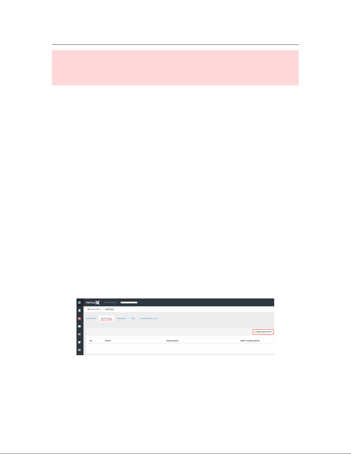
an account using valid email address. Go to your dashboard and click on ’Application’ tab and than
press ’Create application’ button (see Figure 5.1).
Figure 5.1: Creating new Application.
Fill out the ’Application name’ and ’Application description’ fields and click ’Submit’. Click on
your newly created application and under ’Nodes’ tab click on the ’Create node’ button.
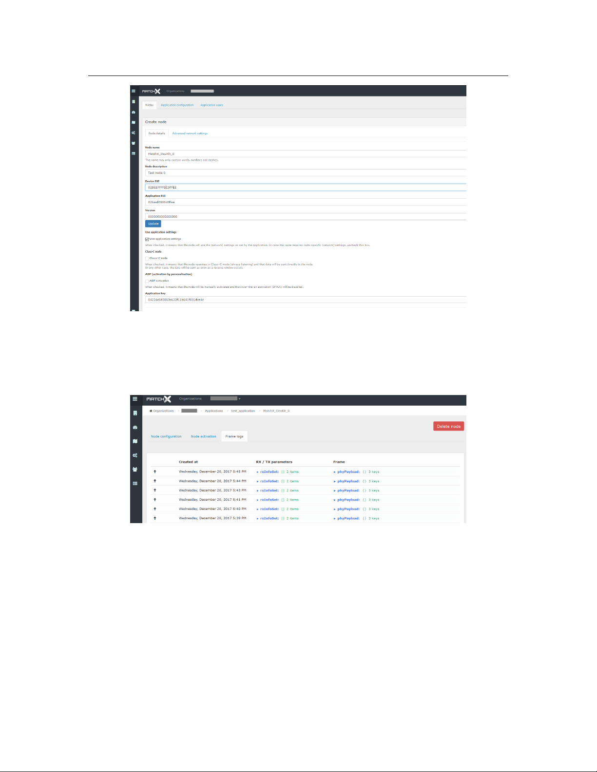
Fill out information about DevKey, DevEUI and AppEUI. Device EUI should be in 64bit format
(with fffe in the middle) like on Figure 5.2. Click on ’Submit’ button. The node is now created, you
Page 27
5.5 Setting DevEUI, AppEUI and DevKey 27
Figure 5.2: Creating new node.
can click on ’View’ under ’Frame Logs’ to see all messages belonging to the node like it is shown
on Figure 5.3.
Figure 5.3: Nodes messages.
5.5 Setting DevEUI, AppEUI and DevKey
To ensure the highest level of security in LoRaWAN network and Over the Air Activation (OTTA) 3
different keys have to be programmed into every end node.
• DevEUI
the end-device, also used by Bluetooth. It is converted to IEEE EUI64 by inserting 0xFFFE in
the bytes 4 and 5. e.g. 78af58fffe040000
• AppEUI
the application provider (i.e., owner) of the end-device
- 6 bytes global end-device ID in IEEE EUI48 address space that uniquely identifies
- 8 bytes global application ID in IEEE EUI64 address space that uniquely identifies
Page 28
28 Chapter 5. Quick Installation Guide
• DevKey - 16 bytes unique AES-128 key
These keys are programmed by MatchX and stored in a special region of the nonvolatile memory
of the Dialog microcontroller. They will be preserved during flashing of the new firmware, however
they will be lost by performing full flash erase. The default values are defined in
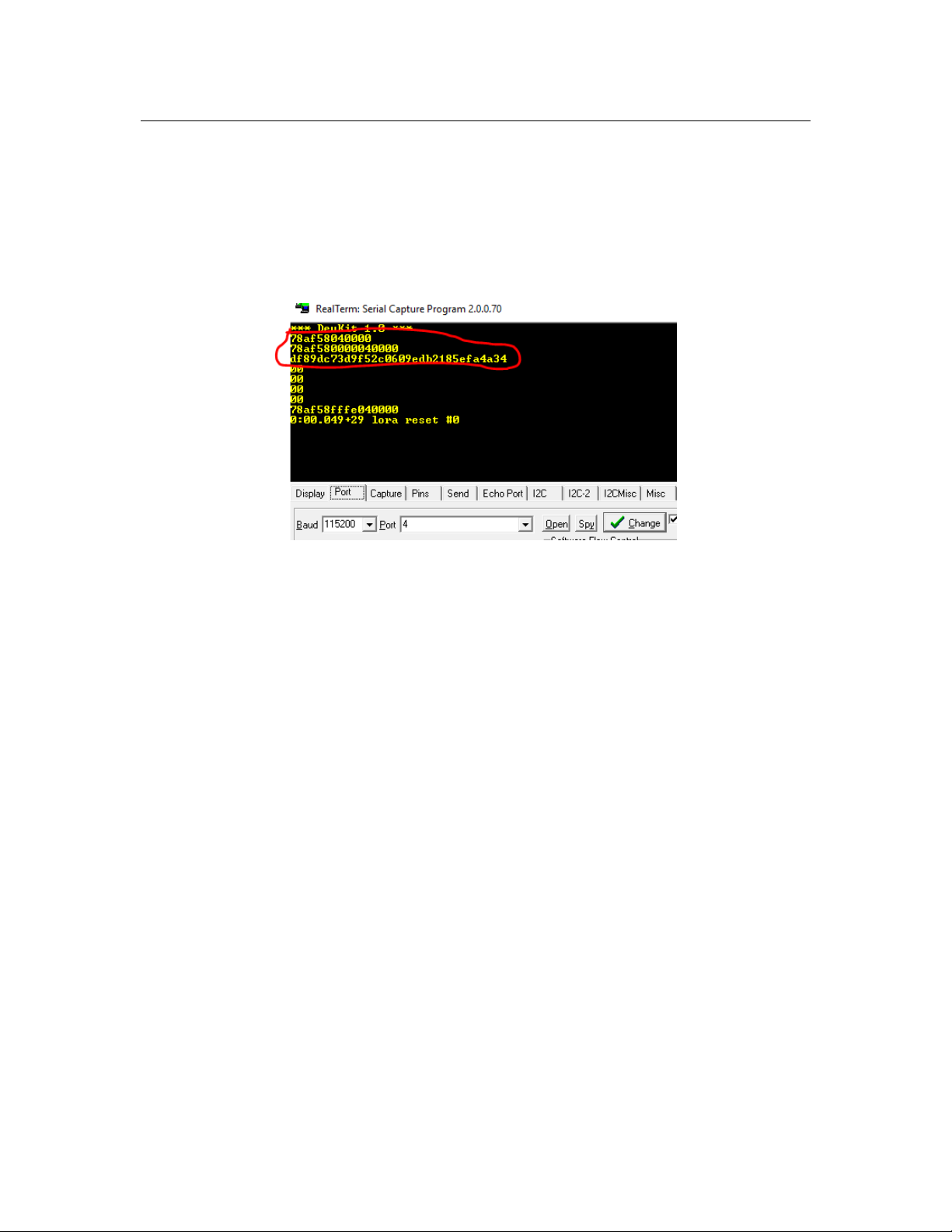
In Dev Kit Firmware the values of these keys are printed on UART console on power up, see Figure
5.4. On default DKF configures pins 5 and 6 on the J102 connector to be UART TX and RX
respectively, a UART-to-USB converter needs to be connected to these pins to see the messages.
lora\param.c
.
Figure 5.4: Displaying the keys on UART console.
The values of DevEUI, AppEUI and DevKey can also be changed from UART console by using
param command. The syntax is as follow:
param x value
where x = 0 for DevEUI, 1 for AppEUI and 2 for DevKey, value is a hexadecimal value to be
set.
When value field is not specified the command will output current value of the parameter
(except DevKey, which will not be shown).
DevKey is a AES-128 encryption key used for secure communication. It should be kept secret
and only known to the sensor owner, this is why it is recommended to not display it on the UART
in a final version of the firmware by removing
recommended to change its value before registering the node on the server.
#define DEBUG
line in
param.c
5.6 Region Selection
Dev Kit Firmware implements different regional settings according to regulations applicable to
these regions. By default the board determines which settings to choose by reading the jumpers
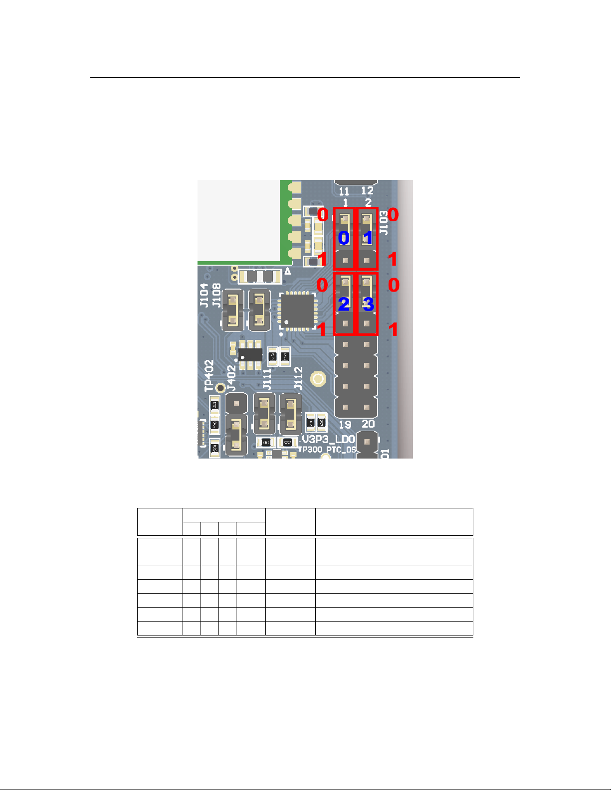
configuration on connector J103 during startup. Jumpers placement is shown on Figure 5.5 and
configuration settings in Table 5.1.
The jumper configuration is read only if the settings are not programmed to internal memory
of the module. It is possible to program these settings using UART similarly to programming the
DevEUI in paragraph 5.5. In this case the jumper values are ignored and J103 pins can be used as
regular GPIOs. The syntax is as follow:
file. It is also
Page 29
5.6 Region Selection 29
param x value
where x = 5 for changing the region, value is a region number in hexadecimal (see Table 5.1).
If value parameter is set to FF firmware will unset regional parameter and the board will return to
reading jumpers settings.
Figure 5.5: Jumpers placement for region selection (EU region selected).
Region Jumper Position
number 3 2 1 0
00 0 0 0 0 EU Europe region
01 0 0 0 1 AS1 Asia AS923MHz ISM Band
02 0 0 1 0 KR Korea region
08 0 1 0 0 US USA region, 8 channels
09 0 1 0 1 AU Australia region, 8 channels
18 1 1 0 0 US(full) USA region, full 64 channels
19 1 1 0 1 AU(full) Australia region, full 64 channels
Table 5.1: Region selection settings.
Region Description
Page 30
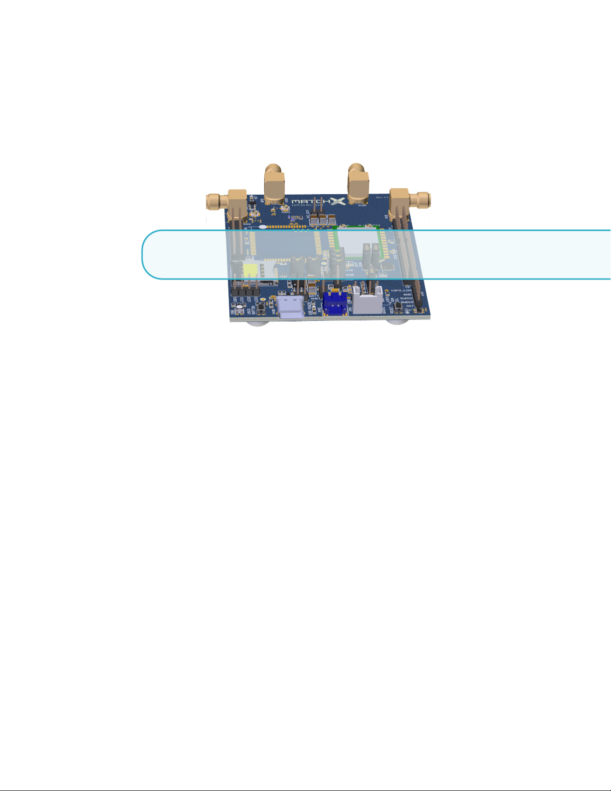
6. Software Development Guide
The purpose of this chapter is to help user to quickly install all necessary software components and
establish hardware connections needed to start software development using MarchX Core SoM and
Development Kit. MatchX is providing the Dev Kit Firmware (DKF) to be a starting point for further
software development according to individual needs.
6.1 References
SoM module is based on Dialog DA14680 microcontroller so it is advisable to get familiar with the
following documents available on Dialog Semiconductors website:
• DA14680-01 DS, Datasheet, Dialog Semiconductor
• UM-B-057-SmartSnippets Studio user guide, User manual, Dialog Semiconductor
• UM-B-047 DA1468x Getting Started, User manual, Dialog Semiconductor
• UM-B-044 DA1468x Software Platform Reference, User manual, Dialog Semiconductor
• UM-B-056 DA1468x Software Developer’s Guide, Dialog Semiconductor
6.2 Prerequisites
• MatchX Development Kit
• USB-C cable and 5V charger
• UART-USB converter
• JLink programmer
• Dialog’s Semiconductor SmartSnippets DA1468x SDK
• SmartSnippets Studio package
• MatchX Dev Kit Firmware
• Operating System (Windows or Linux)
Page 31
6.3 Software development under Windows OS 31
6.3 Software development under Windows OS
The easiest way to install and configure all required tools is to install Dialogs SmartSnippets Studio
package (it can be downloaded from the company website after registration). Experienced users can
try to install all cross-compilation tools and configure they favorite SDE manually, but using Dialogs
software the whole process is straight forward. Please follow UM-B-057 User Manual from Dialog
for details about the installation.
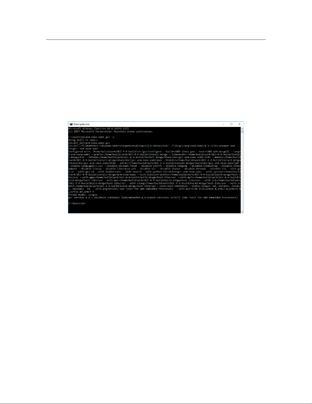
After successful installation of SmartSnippets Studio and J-Link programmer, you should
have gcc cross-compilation tools installed and proper PATH entry should exist, to check it you can
open command line window and type
to what is shown on Figure 6.1. In these example we are using gcc version 4.9.3 20150529.
arm-none-eabi-gcc -v
The result should be similar
Figure 6.1: Checking ARM tools installation.
Download the Dialog’s Semiconductor SmartSnippets DA1468x SDK (in the example the SDK
version 1.0.8.1050.1 has been used) and MatchX Dev Kit Frmware. Both SDK and Dev Kit Firmware
should be put in one folder (for example SmartSnippet workspace folder). DKF folder contains
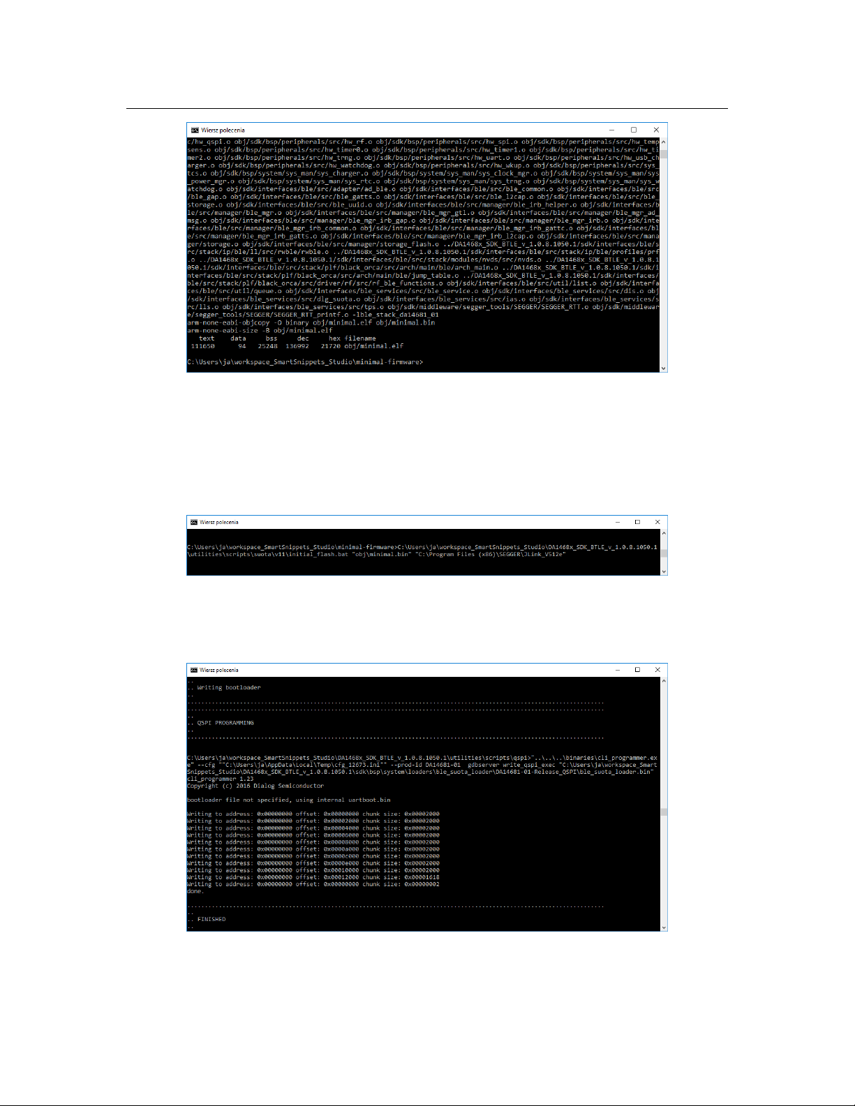
a make file which can be executed by navigating to the firmware folder and typing
command line window. This command will compile the firmware. If everything has been setup
correctly the compilation process should return no errors and a binary file should be generated as a
result, see Fugure 6.2.
After the software has been successfully compiled it can be programmed through J-Link programmer using a script provided by Dialog Semi. In command line window navigate to the DKF
folder. The programming script initial_flash.bat should be located in SDK folder:
DA1468x_SDK_BTLE_v_1.0.8.1050.1\utilities\scripts\suota\v11\
It takes two parameter - path to the .bin file with firmware and path to the J-Link tools. The syntax is
as follows:
{Path}\initial_flash.bat "{Path to firmware}" "{Path to J-Link}"
The example of the command can be seen on Figure 6.3. Before executing it the Dev Kit board has
to be powered on and J-Link programmer has to be connected to SWD port on J101. Only GND,
SWDCK and SWDIO are necessary to program the board. After successful programming process
the screen should look similar as on Figure 6.4. On default DKF configures pins 5 and 6 on the
J102 connector to be UART TX and RX respectively. By connecting a UART-to-USB converter to
make
in the
Page 32
32 Chapter 6. Software Development Guide
Figure 6.2: Compilation process of DKF.
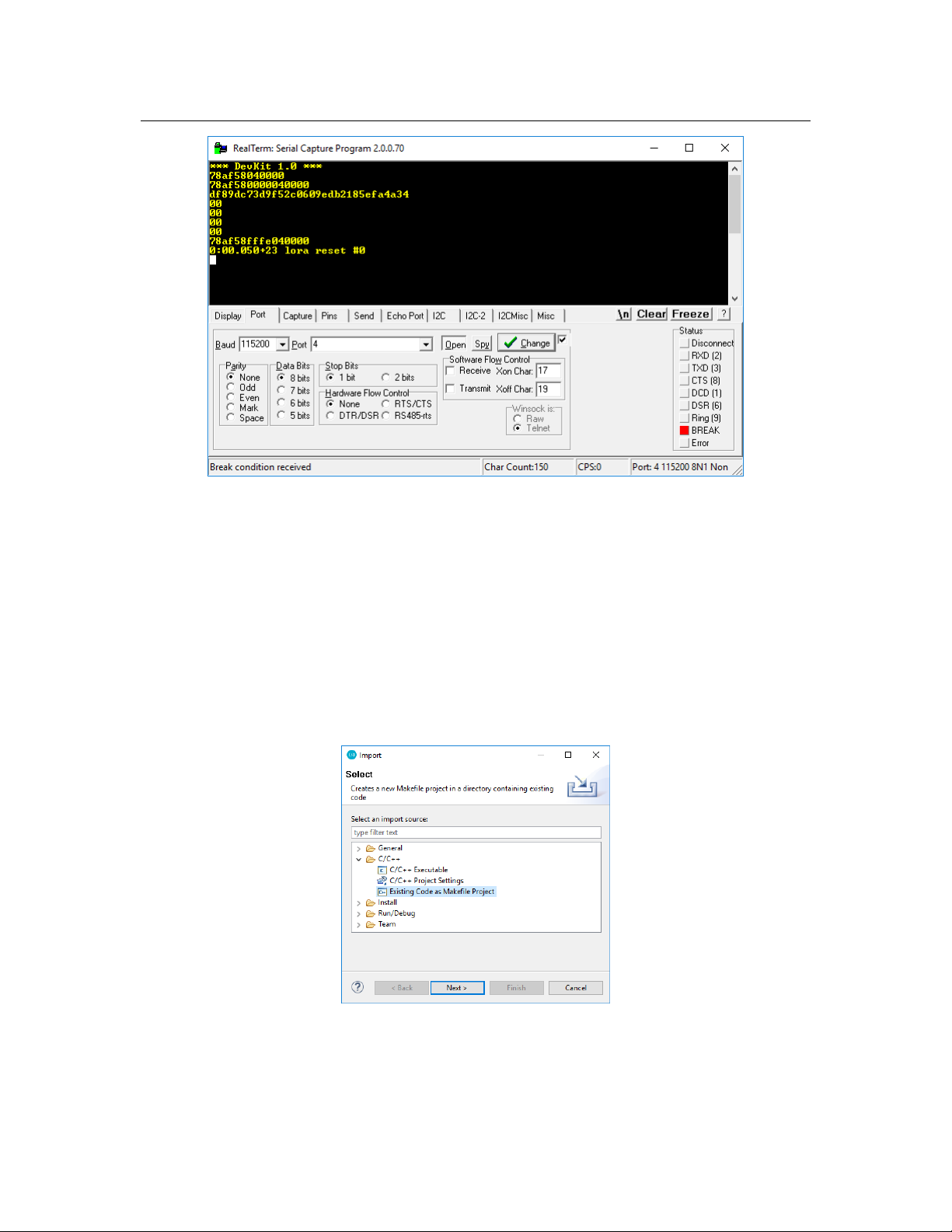
these pins the firmware will output the console messages. The output information sent after reset
and UART configuration can be seen on Figure 6.5.
Figure 6.3: Example of programming command.
Figure 6.4: Programming completed successfully.
Page 33
6.3 Software development under Windows OS 33
Figure 6.5: Console output of the Dev Kit after reset.
6.3.1 Using SmartSnippet Studio
As MatchX DKF is a makefile based project it is possible to port it quite easily to different IDE and
use different operating systems. SmartSnippet Studio is a Dialog Semiconductors IDE based on
Eclipse. It offers makefile project import capabilities.
In order to import the project, open the SmartSnippet IDE. The folder structure should be the
same as in previous section, both SDK and DKF should be in SmartSnippet workspace folder. Go to
File->Import and choose ’Existing Code as Makefile Project’ like on Figure 6.6.
press
Click
Finish
Figure 6.6: Import makefile project window.
Next
. On the next window navigate to the DKF folder. Choose
. The software should be correctly imported and you should be able to compile it by
’Cross ARM GCC’
and
Page 34
34 Chapter 6. Software Development Guide
going to Project->Build All or pressing the build icon.
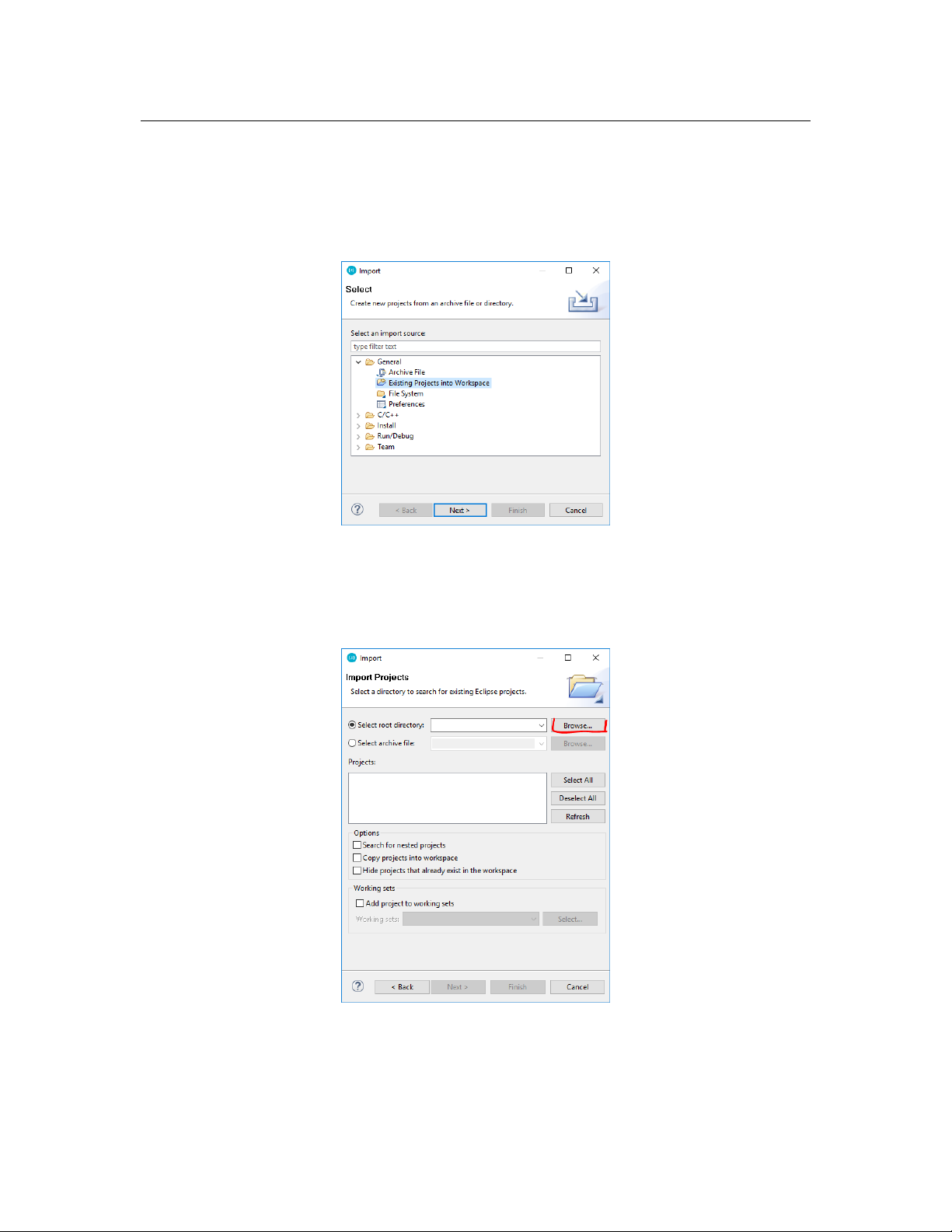
To program the just compiled firmware into DK you need to import "scripts" project to your
workspace. To do that go to
Figure 6.7.
File->Import
Figure 6.7: Import existing project window.
and choose
’Existing Projects into Workspace’
like on
Click
Next
. On the next window navigate to the script folder that should be located in
<sdk_root>\utilities\scripts. See Figure 6.8 and Figure 6.9
Figure 6.8: Importing eXisting project browse window.
Now all the scripts should be available, but in order to use them they must be slightly modified
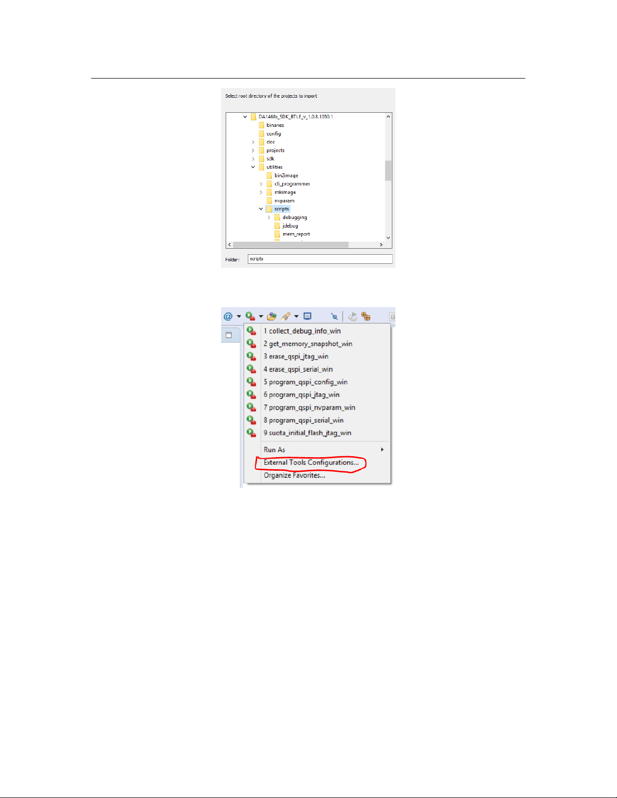
to point to a correct .bin file. Click on ’External Tools Configuration’ as shown on Figure 6.10.
Page 35
6.3 Software development under Windows OS 35
Figure 6.9: Browse window.
Figure 6.10: Scripts.
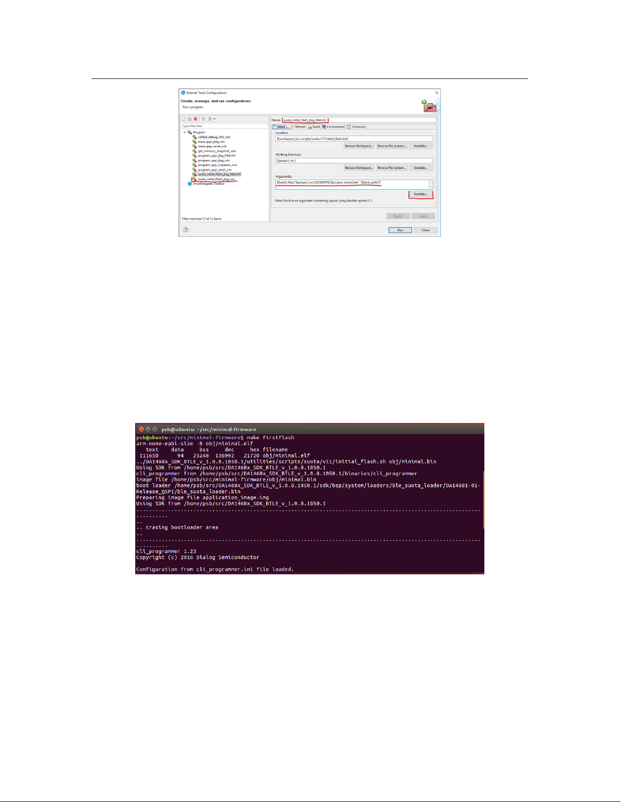
It is best to copy the
’Duplicate’
to compiled firmware. The variables values can be modified by clicking
compiled .bin file is stored in obj folder in the project directory.
then renaming it. The
’suota_initial_flash_jtag_win’
’Argument’
section has to be modified to contain correct path
script by right clicking on it and pressing
’Variables’
button. The
Page 36
36 Chapter 6. Software Development Guide
Figure 6.11: Scripts editing.
6.4 Software development under Linux
Software developing under Linux operating system is straight forward. The easiest way to setup the
environment is to install the the SmartSnippet Studio from Dialog and following the installation
guide in
DA1468x SDK (in the example the SDK version 1.0.8.1050.1 has been used) and MatchX Dev Kit
Frmware. Both SDK and Dev Kit Firmware should be put in one folder (for example SmartSnippet
workspace folder). Open the terminal and navigate to DKF folder. The project contains make file
that takes over the compilation process. The firmware will be compiled by invoking
Programming the DK board is done by invoking make command with firstflash parameter.
UM-B-057
User guide from Dialog. Download the Dialog’s Semiconductor SmartSnippets
make
command.
Figure 6.12: Programming Dev Kit board under Linux OS.
Page 37
7. Product specification
The LPWAN Dev Kit is designed for enhanced LPWAN performance and manageability. In this
chapter we briefly introduce the specifications for both hardware and software.
7.1 Software environment
To facilitate an easy network deployment, we have included many software features, which include
but are not limited to:
• Open source SDK and software support
• Over The Air software update
• Mobile App for Android
• Free cloud service for managing and visualizing sensors data
7.2 Hardware environment
The MatchX Dec Kit is mainly designed for developers and designers for evaluation purposes. It
helps to kickstart your project by providing test and evaluation hardware for proof of concept and
enables programmers to develop software before custom hardware is ready. Using the exchangeable
sensors provides incredibe flexibility so the Dev Kit can be used for many different applications.
Page 38
38 Chapter 7. Product specification
Item Description
MCU DA14680, 0 Hz up to 96 MHz 32-bit ARM Cortex-M0
Memory 8Mb Flash, 64kB OTP, 128kB ROM, 144kB SRAM
Interfaces I2C, I2S, PCM, SPI, UART, USB, GPIOs
Wireless Bluetooth 4.1 and LoRa
Battery 2.0mm pitch connector
Size 32 x 148 x 32mm (including Hat)
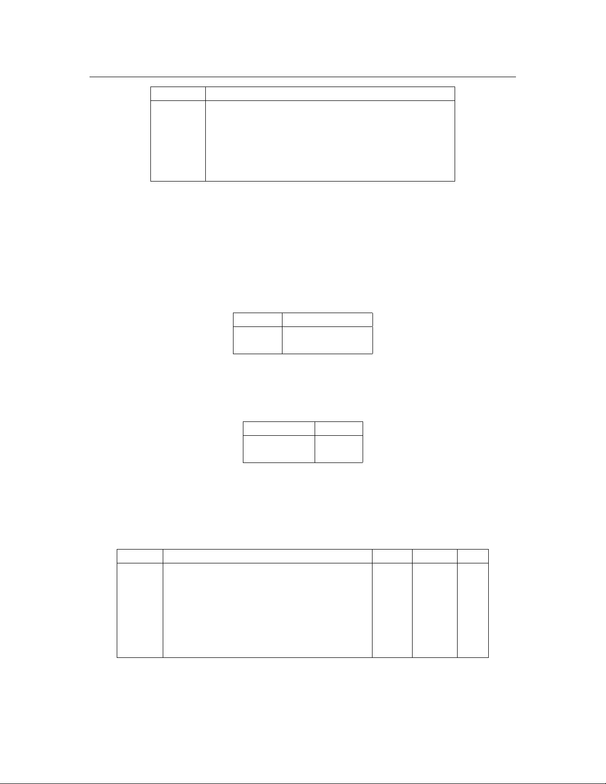
7.2.1 RF performance
There are two RF systems in the module, which include Lora, and Bluetooth. In this section we
briefly introduce the performance of these systems. For Lora, both the "transmission" and "receive"
performance are listed in Table 7.2 and "Bluetooth" can be found in Table 7.3.
Table 7.1: Key hardware specifications
.
Item Value
TX Max +18.5dBm
RX down to -148dBm
For Bluetooth is listed in Table 7.3.
7.2.2 Electrical characteristics
Symbol Description Min Max Unit
V
V
I
V
V
V
I
BUS
T
BATT
SNR
SNR
GPIO
BUS
op
Battery voltage 2.7 4.2 V
Voltage output on the USB-C A8 and B8 pins V
Current output of 3V3_SNR 0 300mA mA
Voltage on any GPIO pin on USB-C 0 V
USB charging voltage 4.2 5.75 V
USB charging current supply 300 mA
Operating Temperature -40 +85
Table 7.2: Lora RF performance
Item Value
Output Power 0dBm
Sensitivity -94dBm
Table 7.3: Bluetooth performance.
BATT
3.3 V
SNR
V
◦
C
Table 7.4: Operating Range.
Page 39
7.2 Hardware environment 39
Symbol Description Min Max Unit
I
IDLE
I
SEN D
I
SLE E P
Current consumption, MCU awake, no RF activity 10 mA
Current consumption,sending LoRa packet 75 mA
Current consumption in sleep mode <10 µA
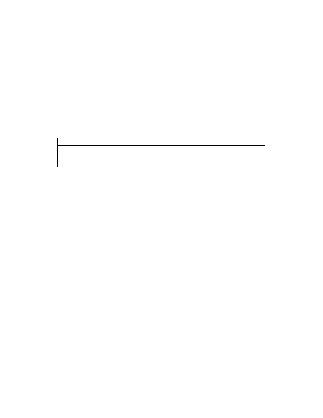
Table 7.5: Current consumption of the core module.
7.2.3 Antenna characteristics
The SoM module is equipped with two U.FL connectors: 2.4GHz for Bluetooth and one for 868MHz
(915MHz in US version) LoRa antenna. The parameters of the recommended antennas can be found
in Table 7.6.
Parameter 2.4GHz antenna 868MHz (EU version) 915MHz (US version)
Center Frequency 2.44GHz 868MHz 915MHz
Bandwidth 101MHz 40MHz 40MHz
Gain 4.3dBi 2.33dBi 2.3dBi
Table 7.6: Parameters of recommended antennas.
Page 40
40 Chapter 7. Product specification
7.3 Dimensions
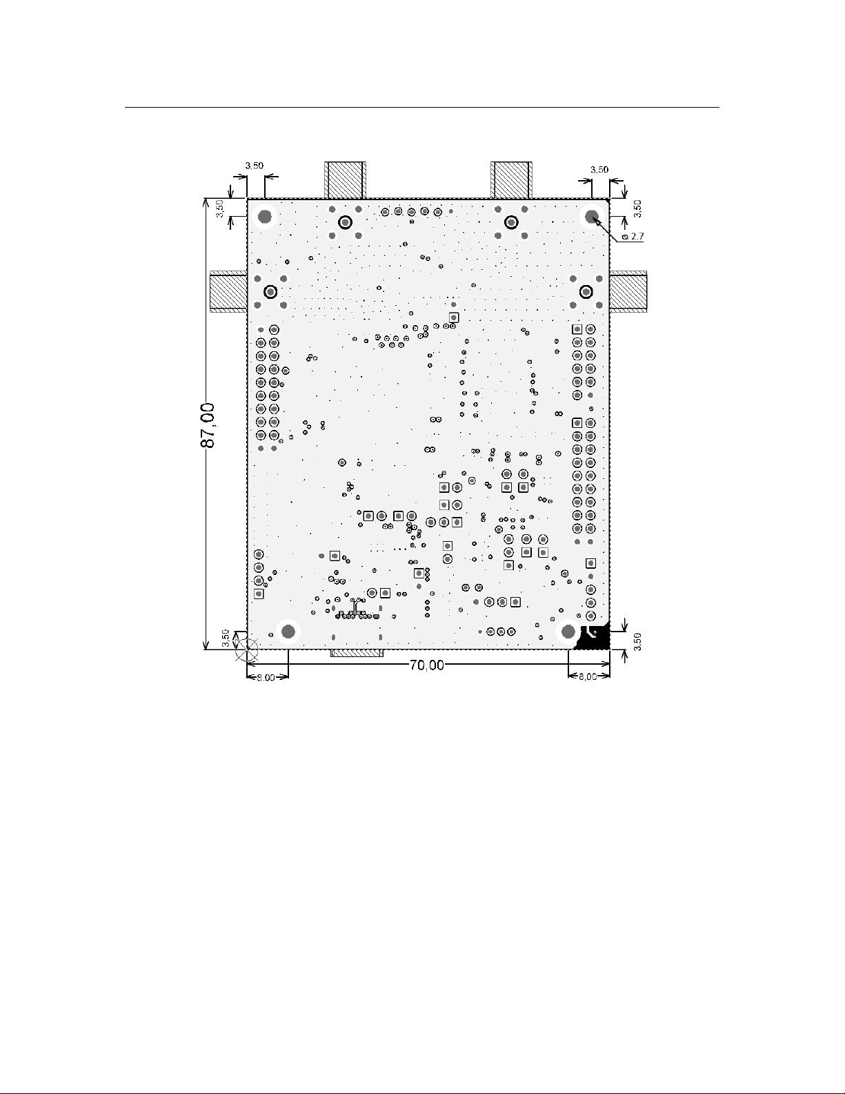
Figure 7.1: Dimension of the Dev Kit (top view), all dimensions in mm.
Page 41

7.4 Certification 41
7.4 Certification
CE and FCC certification pending.
 Loading...