

120 Broadway Menands, New York 12204
Toll Free: (800) 98-4LEDS Fax: (518) 432-7454
marktech
optoelectronics
TOSHIBA
TOSHIBA Bi-CMOS INTEGRATED CIRCIUTS SILICON MONOLITHIC
T B 6 2 7 2 5 P / F / FN
T B 6 2 7 2 5 P / F / F N
TB62725 series is the constant current driver designed
for LED and the LED displ a
y
. Output current value is
set with one resistor with the outside.
Then, all the output becomes the about same current.
This driver builds in the constant current output of
ei
g
ht bits, the shift register of eight bits, the latch of
ei
g
ht bits and gate circuit.
This driver is desi
g
ned by using the BI-CMOS process.
FEATURE
*Output Current Capabilit
y
and the number of the output :
90mA X 8 outputs
*Constant Current Ran
g
e : 5 to 90mA
*Application Output Volta
g
e :
0.7V
(
output current 40 to 80 mA
)
0.4V (output current 5 to 40 mA
)
*For Annode Common LED
*Input Si
g
nal Voltage Lev el :
3.3V CMOS Level
(
Shmitt Triggered Inp ut
)
*Power Supply Voltage Range VDD=3.0 to 3.6V
*Muximum output terminal volta
g
e 17V
*Serial and Pararell Data Transfer Rate :
20MHz
(
max, Cascade Connection
)
*Operation Temperature Range :
Topr= -40 to 85 de
g
rees
*Packa
g
e :
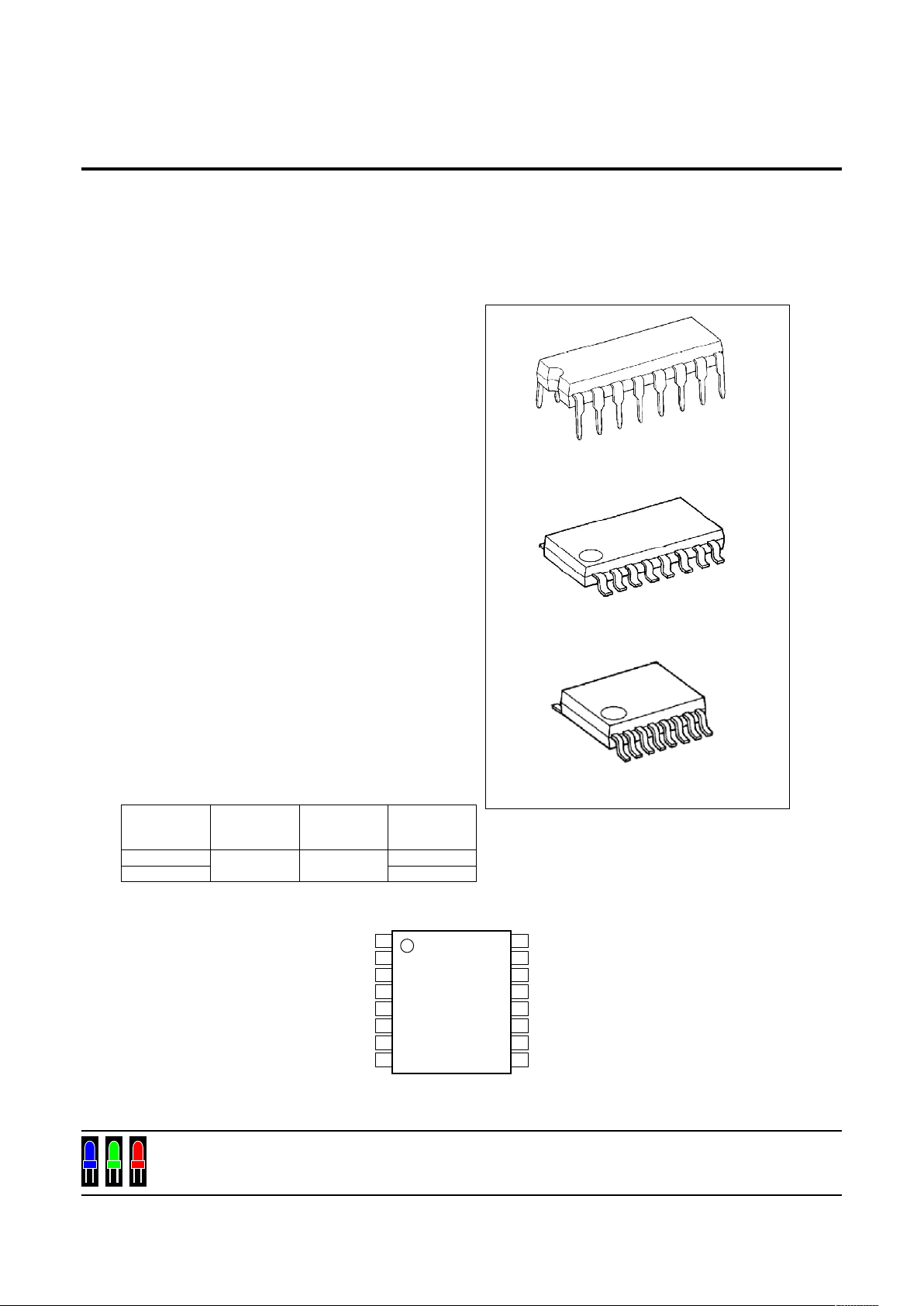
T
y
pe P : DIP16-P-300-2.56A
T
y
pe F : SSOP16-P-225-1.00
T
y
pe FN : SSOP16-P-225-0.65
*Packa
g
e and Pin Layout : Same as the TB62705 series.
*Constant Current Error bitween bits
(
All Output On
)
Pin layout (TOP VIEW
)
Output
Voltage
Current
Error
between bits
Current
Error
between ICs
Output
Current
>= 0.4V +/- 6% +/- 15% 2 to 40 mA
>= 0.7V 2 to 90 mA
GND
SERIAL-IN
CLOCK
/LATCH
OUT0
OUT1
OUT2
OUT3
VDD
R-EXT
SERIAL-OUT
/ENABLE
OUT7
OUT6
OUT5
OUT4
8BIT CONSTANT CURRENT LED DRIVER OF OPERATING VOLTAGE 3.3V
TB62725P
TB62725F
TB62725FN
DIP16-P-300-2.56A
SSOP16-P-225-1.00
SSOP16-P-225-0.65
Weight : 1.11 g(Typ.) - - - Type P
0.14 g(Typ.) - - - Type F
0.07 g(Typ.) - - - Type FN
120 Broadway Menands, New York 12204
Toll Free: (800) 98-4LEDS Fax: (518) 432-7454
marktech
optoelectronics
TOSHIBATOSHIBA
T B 6 2 7 2 5 P / F / FN
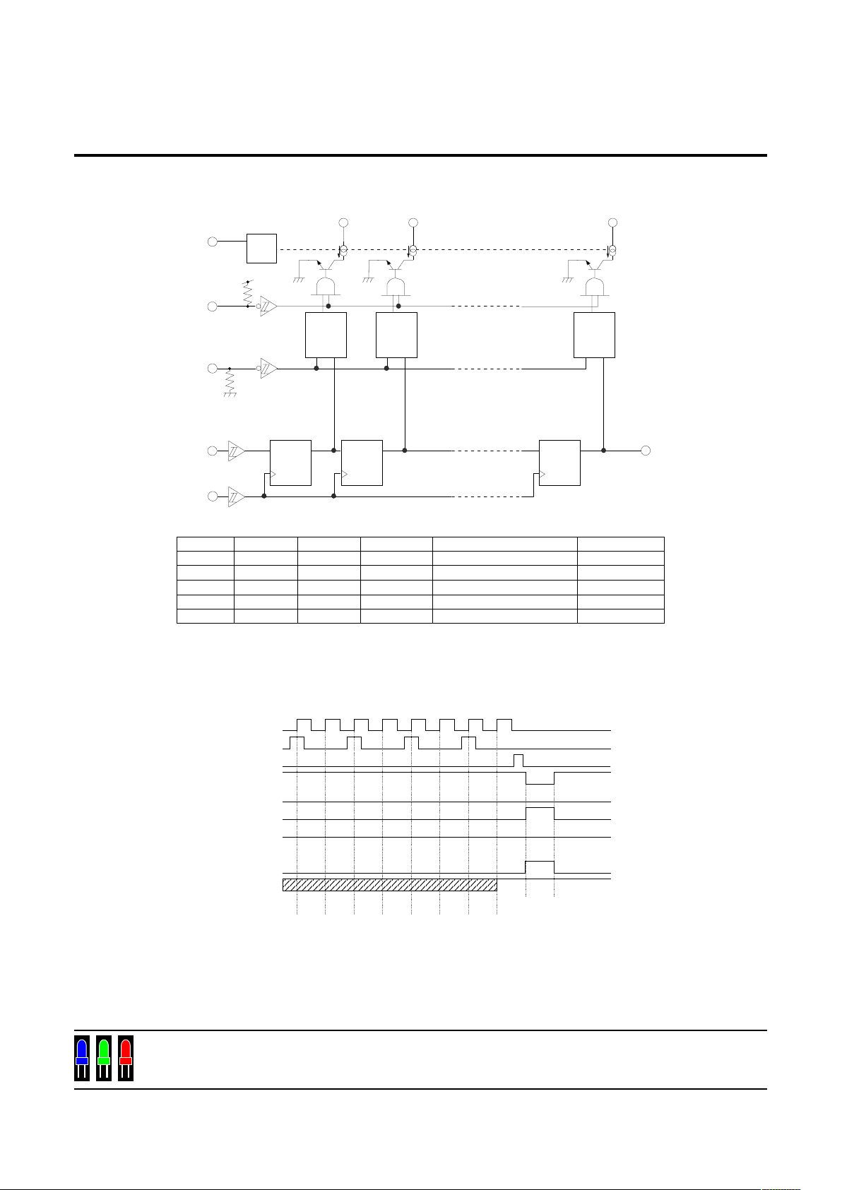
CLOCK /LATCH /ENABLE SERIAL-IN OUT0 --- OUT5 --- OUT7 SERIAL-OUT
UP H L Dn Dn --- Dn-5 --- Dn-7 Dn-7
UP L L Dn+1 No Change Dn-6
UP H L Dn+ 2 Dn+2 --- Dn-3 --- Dn-5 Dn-5
DOWN X L Dn+3 Dn+2 --- Dn-3 --- Dn-5 Dn-5
DOWN X H Dn+3 Off Dn-5
BLOCK DIAGRAM
R-EXT
/ENABLE
/LATCH
SERIAL-IN
CLOCK
OUT0 OUT1 OUT7
SERIAL-OUT
I-REG
Q
ST D
Q
ST D
Q
ST D
DQCKDQ
CK
DQ
CK
TRUTH TABLE
Note) "OUT0 to 7 = On" in case of Dn= "H" Level and "OUT0 to 7 = Off" in case of Dn= "L" Level.
A resistor is connected with R-EXT and GND accompanied with outside, and it is necessary that a correct power
supply voltage is supplied.
TIMING DIAGRAM
CLOCK
SERIAL-IN
/LATCH
/ENABLE
OUT0
OUT1
OUT3
OUT7
SERTIAL-OUT
Note) Latches are level sensitive, not rising edge sensitive and not syncronus CLOCK.
Input of LATCH-terminal to "H" level, data passes latches and input to "L" level, data hold latches.
Input of ENABLE-terminal to "H" level, all output ( OUT0 to 7 ) off.
5V
0V
5V
0V
5V
0V
5V
0V
On
Off
On
Off
On
Off
On
Off
5V
0V
120 Broadway Menands, New York 12204
Toll Free: (800) 98-4LEDS Fax: (518) 432-7454
marktech
optoelectronics
TOSHIBATOSHIBA
T B 6 2 7 2 5 P / F / FN
PIN No. PIN NAME FUNCTION
1 GND GND terminal for control logic.
2 SERIAL-IN Input terminal of a serial-data for shift-register
3 CLOCK Input terminal of a clock for data shift to up-edge.
4 /LATCH
Input terminal of a data strobe. Latches passes data with "H" level
input of
LATCH-terminal, and hold data with "L" level input.
5~12 OUT0 to 7 Output terminals.
13 /ENABLE
Input terminal of output enable. All outputs (OUT0 to 7) do off with "H" level input
of ENABLE-terminal, and do on with "L" level input.
14 SERIAL-OUT Output terminal of a serial-data for next SERIAL-IN terminal.
15 R-EXT Input terminal of connects with a resister for to set up all output current.
16 VDD 5V Supply voltage terminal
/ENABLE
VDD
GND
VDD
GND
/LATCH
VDD
GND
CLOCK,
SERIAL - IN
VDD
GND
8th DATA
SERIAL - OUT
EQUIVALENT CIRCUIT OF INPUTS AND OUTPUTS
1. /ENABLE Terminal
2. /LATCH Terminal
3. CLOCK,SERIAL-IN Terminal
4. SERIAL-OUT Terminal
R(UP)
R(DOWN)
TERMINAL DISCRIPTION
GND
OUT 0 to 7
5. OUT0 to 7 Terminal
120 Broadway Menands, New York 12204
Toll Free: (800) 98-4LEDS Fax: (518) 432-7454
marktech
optoelectronics
TOSHIBATOSHIBA
T B 6 2 7 2 5 P / F / FN
RECOMMENDED OPERATING CONDITION (Ta=-40 to 85degC unless otherwise noted)
CHARACTERISTICS SYMBOL RATING UNIT
Suppl y Voltage VDD 0 to 7 V
Input Voltage VIN -0.2 to VDD+0.2
Output Current IOUT +90 mA/ch
Output Voltage VOUT -0.5 to 17 V
Power Dissipati on Pd1 Type P : 1.47(Free Air) W
Pd2 Type F and FN : 0.37 (Free Air), 0.78 (On PCB)
Thrmal Resistance Rth(j-a)1 Type P : 85(Free Air) degC/W
Rth(j-a)2 Type F and FN : 330 (Free Air),160 (On PCB)
Oparating Temperature Topr -40 to 85 degC
Storage Temperature Tstg -55 to 150
CHARACTERISTICS SYMBOL CONDITION MIN. TYP. MAX. UNIT
Supply Voltage VDD 3 3.3 3.6 V
Output Voltage VOUT 0.7 4 V
Output Current IOUT Each DC 1 Circuit 2 70 mA/ch
IOH SERIAL-OUT -1 mA
IOL 1
Input Voltage VI H 0.7VDD
VDD
+0.15
V
VIL -0.15 0.3VDD
Clock Frequency fCLK Cascade Connected 20 MHz
/LATCH Pulse Width tw /LATCH 50
CLOCK Pulse Width tw CLOCK 25
/ENABLE Pulse Width tw /ENABLE
Upper IOUT = 20 mA
2000
Lower IOUT = 20 mA 4500
Setup Tim e
for CLOCK Terminal
tsetup1 10 ns
Hold T im e
for CLOCK Terminal
thold 5
Setup Tim e
for /LATCH Terminal
tsetup2 50
MAXIMUM RATINGS ( Ta = 25degC )
Note) Type P : Ambient temperature delated above 25degC in the proportion of 11.76 mW/degC.
Type F and FN : Ambient temperature delated above 25degC in the proportion of 7.69 mW/degC.
Condition) On PCB at 50 X 50 X 1.6mm Cu <= 40% ( Glass Epoxy PCB )
120 Broadway Menands, New York 12204
Toll Free: (800) 98-4LEDS Fax: (518) 432-7454
marktech
optoelectronics
TOSHIBATOSHIBA
T B 6 2 7 2 5 P / F / FN
ELECTRICAL CHARACTERISTICS (VDD=3.3V, Ta=25degC unless otherwise noted)
SWITCHING CHARACTERISTICS (Ta=25degC unless otherwise noted)
CHARACTERISTICS SYMBOL CONDITION
MIN
TYP MAX UNIT
Supply Voltage VDD Normal Operation
3.0
3.3 3.6 V
Output Current IOUT1 VOUT=0.4V,REXT=490ohms 31.9 37.5 43.1 mA
IOUT2 VOUT=0.7V,REXT=250ohms 62.6 73.6 84.6
Output Current dIOUT1
VOUT>=0.4V,REXT=490ohms
All outout on.
+/-1.5 +/-6 %
Error bit ween bits dIOUT2
VOUT>=0.7V,REXT=250ohms
All outout on.
+/-1.5 +/-6
Output Leakage
Current
IOZ VOUT=15.0V 1.0 5.0 uA
Input Voltage VIH
0.7
VDD
VDD
VIL GND
0.3
VDD
SOUT Terminal VOL IOH=+1mA 0.4 V
Output Voltage VOH IOL=-1mA 2.8
Output Currnet
Supply Voltage
Reguration
%/VDD VDD = 3V to 3.6V +/-1.5 +/-5.0 %
Pull up Resistor R(up) /ENABLE Terminal 100 200 400 kohms
Pull down Resistor R(down) /LATCH Terminal 125 250 500
IDD(OFF)1 REXT=OPEN,VOUT=15.0V 1 2
IDD(OFF)2
REXT=490Ohms,
VOUT=15V,OUT0 to 7 are Off.
1 3 5
Supply Current IDD(OFF)3
REXT=250Ohms,
VOUT=15V,OUT0 to 7 are Off.
3 6 8 mA
IDD(ON)1
REXT=490Ohms,
VOUT=0.7V,OUT0 to 7 are On.
7
Same as the avobe , Ta=-40degC 14
IDD(ON)2
REXT=250Ohms,
VOUT=0.7V,OUT0 to 7 are On.
13
Same as the avobe , Ta=-40degC 25
CHARACTERISTICS SYBOL TEST CONDITION MIN TYP MAX UNIT
tpLH1
CLK - OUTn,
/LATCH="H",/ENABLE="L"
140
tpLH2 /LATCH - OUTn,
/ENABLE="L"
140
tpLH3 /ENABLE - OUTn,
/LATCH="H"
140
Propagation tpLH CLK - SERIAL OUT 5
Delay Time tpHL1
CLK - OUTn,
/LATCH="H",/ENABLE="L"
170
tpHL2 /LATCH - OUTn, /ENABLE="L" 170 ns
tpHL3
/ENABLE - OUTn, /LATCH="H"
170
tpHL CLK - SERIAL OUT 6
Output Rise Time t or Voltage Waveform 10% to 90% 70
Output Fall Time t of Voltage Waveform 90% to 10% 90
Muxi mu m CLOCK
Rise Time
tr Cascade connecti on isn't guarantee. 5 us
Muxi mu m CLOCK
Fall Time
tf (Note1) 5
Condition : (Refer to test circuit.)
Ta= 25 degC, VDD=VIH=3.3V, VOUT=0.7V, VIL=0V, REXT=490ohms, VL=3.0V, RL=60ohms, CL=10.5pF
Note 1 : When tf / tf of clock wave form is enlarged at the time as the cascade connection,
the timing condition which is necessary for the data transfer may not be able to be secured.
Give careful consideration to the timing condition.

120 Broadway Menands, New York 12204
Toll Free: (800) 98-4LEDS Fax: (518) 432-7454
marktech
optoelectronics
TOSHIBATOSHIBA
T B 6 2 7 2 5 P / F / FN
IDD
IOL
VIH,VIL
R-EXT
SERIAL-IN
/LATCH
CLOCK
OUT0
OUT7
SERIAL-OUT
/ENABLE
VDD
RL
CL
CL
VL
GND
TEST CIRCUIT
Iref
Function
Generator
VDD=VIH=3.3V
VIL=0V
tr = tf = 10ns
(10% to 90%)
LOGIC
INPUT WAVEFORM

120 Broadway Menands, New York 12204
Toll Free: (800) 98-4LEDS Fax: (518) 432-7454
marktech
optoelectronics
TOSHIBATOSHIBA
T B 6 2 7 2 5 P / F / FN
TIMING WAVEFORM
tw CLK
tpLH/tpHL
50%50%
50%
50%
50%
1. CLOCK ,SERIAL-IN, SERIAL-OUT
CLOCK
SERIAL IN
SERIAL-OUT
2. CLOCK, SERIAL-IN , /LATCH, /ENABLE, OUTn
t HOLD
50%
CLOCK
SERIAL IN
/LATCH
50% 50%
tw LAT
t SETUP1
t SETUP2
/ENABLE
50% 50%
tw ENA
t SETUP2
50%
tpHL3/LH3
tpHL2/LH2
tpHL1/LH1
OUTn
3. OUTn
tof tor
90% 90%
10% 10%
OUTn

120 Broadway Menands, New York 12204
Toll Free: (800) 98-4LEDS Fax: (518) 432-7454
marktech
optoelectronics
TOSHIBATOSHIBA
T B 6 2 7 2 5 P / F / FN
020406080100
DUTY - Turn On Rate (%)
0
10
20
30
40
50
60
70
80
90
100
IOUT(m A)
TB62725F/FN
TB62725P
DUTY(%)-IOUT(mA) On PCB
Topr=25degC
VDD=3.3V, Vce=1.0(V), Tj=120(degC max)
020406080100
DUTY - Turn On Rate (%)
0
10
20
30
40
50
60
70
80
90
100
IOUT(m A)
TB62725F/FN
TB62725P
DUTY(%)-IOUT(mA) On PCB
Topr=55degC
VDD=3.3V, Vce=1.0(V), Tj=120(degC max)
0 20406080100
DUTY - Turn On Rate (%)
0
10
20
30
40
50
60
70
80
90
100
IOUT(m A)
TB62725F/FN
TB62725P
DUTY(%)-IOUT(mA) On PCB
Topr=85degC
VDD=3.3V, Vce=1.0(V), Tj=120(degC max)
OUTPUT CURRNET vs Duty (LED Turn On Rate)

120 Broadway Menands, New York 12204
Toll Free: (800) 98-4LEDS Fax: (518) 432-7454
marktech
optoelectronics
TOSHIBATOSHIBA
T B 6 2 7 2 5 P / F / FN
020406080100
DUTY - Turn On Rate (%)
0
10
20
30
40
50
60
70
80
90
100
IOUT(mA)
TB62725F/ FN
TB62725P
TB62705CF/CFN
TB62705CP
TB62705 & 725 DUTY(%)-IOUT(mA) On PCB
Topr=25degC
VDD=5.0V, Vce=1.0(V), Tj=120(degC max)
0 20406080100
DUTY - Turn On Rate (%)
0
10
20
30
40
50
60
70
80
90
100
IOUT(mA)
TB62725F/FN
TB62725P
TB62705CF/CFN
TB62705CP
TB62705 & 725 DUTY(%)-IOUT(mA) On PCB
Topr=55degC
VDD=5.0V, Vce=1.0(V), Tj=120(degC max)
0 20406080100
DUTY - Turn On Rate (%)
0
10
20
30
40
50
60
70
80
90
100
IOUT(mA)
TB62725F/FN
TB62725P
TB62705CF/CFN
TB62705CP
TB62705 & 725 DUTY(%)-IOUT(mA) On PCB
Topr=85degC
VDD=5.0V, Vce=1.0(V), Tj=120(degC max)
0102030405060708090100
110
120
130
140
150
Ambient Temperature Ta (deg)
0
0.2
0.4
0.6
0.8
1
1.2
1.4
1.6
Power dissipation PD (W/IC)
1: F/FN(OnPCB)
2: P(FreeAir)
Ta(degC) - Pd(w)
OUTPUT CURRNET vs Duty (LED Turn On Rate)
** Comparison in VDD=5V of TB62705 and TB6272

120 Broadway Menands, New York 12204
Toll Free: (800) 98-4LEDS Fax: (518) 432-7454
marktech
optoelectronics
TOSHIBATOSHIBA
T B 6 2 7 2 5 P / F / FN
OUTPUT CURRNET vs REXT RESISTOR
APPLICATION NOTES(1 of 2)
Thi s devic e owns onl y one ground pin that means signal gr ound pin an d power g round pin are com mon.
If ground pattern layout contains large inductance and impedance, and the voltage between ground and LATCH, CLOCK terminals
exceeds 0.5* Vdd by switc hing noise in operat ion, t his device m ay m iss-oper ate.
So we would lile you to pay attention to pattern layout to minimize inductance.
TB62725P/F/FN application circuit (a general example)
TB62725 Series recommend VLED=VDD= 3.3(V min) and data transfer of fclk=20(MHz ) is possible at cascade connection.
1 : Vf of LED is Vf=2.5 (V max).
2 : Output saturation Vce1 = 0.4(V min) at Iout <= 40(mA) of TB62725.
3 : Output saturation Vce2 = -0.25(V max) at Ic = -1(A) of TD62M8600F.
4 : TB62725 can move with VDDopr = 3 to 3.6(V).
5 : When a necessary voltage to 1 from 3 is summed up,
the t otal voltage is le ss than 3.3(V),
and this circuit can move with VLED = VDD = 3.3 (V min).
S-IN
CLK
LAT
ENA
S-OUT
O
0O1O2
O5O6O
7
O0O1O
2
O5O6O
7
SCAN
S-IN
CLK
LAT
ENA
S-OUT
VLED
C.U.
r1 : Resi stance for a setup of output current.
r2 : Re sistance for the LED module brightness adjustment.
r1r1
r2
Example) TD62M8600F
8-bit Multi-Chip PNP Tr Array,
which i s not used i n Stat ic Li ghting Sys tem.
8 -bit SIPO,Latches &
Constant Sink Current Drivers
8-bit SIPO,Latches &
Constant Sink Current Drivers
TB62725P/F/FN
Not C onnect Resistor
TB62725P/F/FN
100 1000 10000
REXT(Ohms)
0
10
20
30
40
50
60
70
80
90
IOUT(mA)
Topr=-40(degC)
Topr=+25(degC)
Topr=+85(degC)
TB62725P/F/FN REXT-IOUT (Topr)
VDD=3.3(V), VCE=0.7( V)
IOUT[mA]=(1.14/REXT[ohms])*16 -- Theory formula

120 Broadway Menands, New York 12204
Toll Free: (800) 98-4LEDS Fax: (518) 432-7454
marktech
optoelectronics
TOSHIBATOSHIBA
T B 6 2 7 2 5 P / F / FN
TB62725P/F/FN application circuit (the case of VLED>17(V) )
Example :
An u nnecessary voltage in the case of VLED>17(V)
makes a volt age des cend by t he Z ener dio de.
S-IN
CLK
LAT
ENA
S-OUT
O
0O1O2
O5O6O
7
O0O1O
2
O5O6O
7
SCAN
S-IN
CLK
LAT
ENA
S-OUT
VLED
C.U.
r1r1
r2
8-bit SIPO,Latches &
Constant Sink Current Drivers
8-bit SIPO,Latches &
Constant Sink Current Drivers
TB62725P/F/FN TB62725P/F/FN
Example) TD62M8600F
8-bit Multi-Chip PNP Tr Array,
which is not used in Static Lighting System.
r1 : Resistance for a setup of output current.
r2 : Resistance for the LED module brightness adjustment.
APPLICATION NOTES(2 of 2)
TB62725P/F/FN application circuit (with VLED<=17(V), the case of the over-saturation)
r3
r3
S-IN
CLK
LAT
ENA
S-OUT
O
0O1O2
O5O6O
7
O0O1O
2
O5O6O
7
SCAN
S-IN
CLK
LAT
ENA
S-OUT
VLED
C.U.
r1r1
r2
8-bit SIPO,Latches &
Constant Sink Current Drivers
8-bit SIPO,Latches &
Constant Sink Current Drivers
TB62725P/F/FN
Example) TD62M8600F
8-bit Multi-Chip PNP Tr Array,
which is not used in Static Lighting System.
r1 : Resistance for a setup of output current.
r2 : Resistance for the LED module brightness adjustment.
TB62725P/F/FN
Example :
An over-satur ation voltage makes a volt age descend by the resist ance with t he outside.
Condition :
1 : Turn on LED with Iout=20(mA).
2 : LED of Vf=2.5( V max).
3 : saturation voltage =0.4(V min) at Ic= 20(mA) of TB62725
4 : saturation voltage =0.25(V min) at Ic= 320(mA) of TD62M8600F
Connec t R1, and decrease the heat l osses o f the IC.
r3= ( 15-0.4-LED Vf*1 - 0.25 ) /20mA =592.5(Ohms)

120 Broadway Menands, New York 12204
Toll Free: (800) 98-4LEDS Fax: (518) 432-7454
marktech
optoelectronics
TOSHIBATOSHIBA
T B 6 2 7 2 5 P / F / FN

120 Broadway Menands, New York 12204
Toll Free: (800) 98-4LEDS Fax: (518) 432-7454
marktech
optoelectronics
TOSHIBATOSHIBA
T B 6 2 7 2 5 P / F / FN

120 Broadway Menands, New York 12204
Toll Free: (800) 98-4LEDS Fax: (518) 432-7454
marktech
optoelectronics
TOSHIBATOSHIBA
T B 6 2 7 2 5 P / F / FN

120 Broadway Menands, New York 12204
Toll Free: (800) 98-4LEDS Fax: (518) 432-7454
marktech
optoelectronics
TOSHIBA
The information contained herein is subject to change without notice.
The information contained herein is presented only as a guide for the applications of our
products. No responsibility is assumed by TOSHIBA for any infringements of patens or other
rights of the third parties which may result from its use. No license is granted by implication
or otherwise under any patent or patent rights of TOSHIBA or others.
TOSHIBA is continually working to improve the quality and the reliability of its products.
Nevertheless, semiconductor devices in general can malfunction or fail due to their inherent
electrical sensitivity and vulnerability to physical stress. It is the responsibility of the buyer,
when utilizing TOSHIBA products, to observe standards of safety, and to avoid situations in
which a malfunction or failure of a TOSHIBA product could cause loss of human life, bodily
injury or damage to property.
In developing your designs, please ensure that TOSHIBA products are used within spacified
operating ranges as set forth in the most recent products spacifications. Also, please keep in
mind the precautions and conditions set forth in the TOSHIBA Semiconductor Reliability
Handbook.
The products described in the document may include products subject to foreign exchange
and foreign trade control laws.
(C) 2000 TOSHIBA CORPORATION
ALL RIGHT Reserved
T B 6 2 7 2 5 P / F / FN
 Loading...