

Page 1
Service
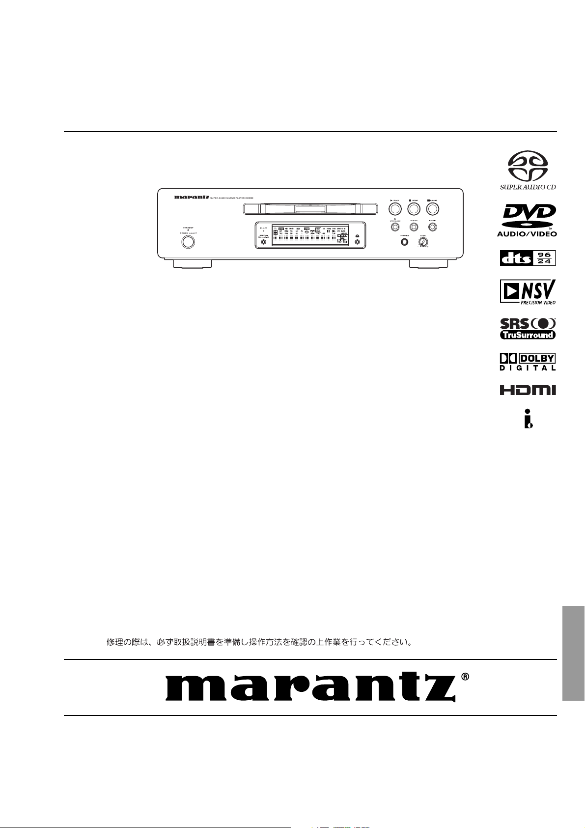
DV9600
DV9600 /
F N/K1G/L1G/S1G
/F B/U1B
/N1S
Manual
SECTION PAGE
1. TECHNICAL SPEC I FI CA TIONS ........................................................................................... 1
2. SERVICE HINTS AND TOOLS ............................................................................................. 6
3. WARNING AND LASER SAFETY IN STRUC TIONS ............................................................. 7
4. TAKING THE DISC OUT OF EMERGENCY......................................................................... 8
5. UPDATE BACK END SOFTWARE (FIRM WARE) PRO CE DURE ......................................... 9
6. UPDATE PANEL MICROPROCESSOR PRO CE DURE ...................................................... 10
7. SER VICE MODE................................................................................................................. 36
8. WRITE-IN ID DATA FOR DVD AUDIO PROCEDURE......................................................... 37
9. TROUBLESHOOTING/(Japan) .................................................................................... 42/(65)
10. WIRING DIAGRAM ............................................................................................................. 87
11. BLOCK DIAGRAM .............................................................................................................. 89
12. SCHEMATIC DIAGRAM...................................................................................................... 91
13. PARTS LOCATION............................................................................................................ 133
14. MI CRO PRO CES SOR AND IC DATA................................................................................. 153
15. EXPLODED VIEW AND PARTS LIST............................................................................... 186
16. ELECTRICAL PARTS LIST .............................................................................................. 194
Super Audio CD / DVD Player
TABLE OF CONTENTS
Please use this service manual with referring to the user guide ( D.F.U. ) without fail.
DV9600
Part no. 90M25AK855010
First Issue 2005.09
MZ
Page 2
MARANTZ DESIGN AND SERVICE
Using superior design and selected high grade components,
Only original
MARANTZ
parts can insure that your
MARANTZ
MARANTZ
product will continue to perform to the specifi cations for which
company has created the ultimate in stereo sound.
it is famous.
Parts for your
MARANTZ
ORDERING PARTS :
equipment are generally available to our National Marantz Subsidiary or Agent.
Parts can be ordered either by mail or by Fax.. In both cases, the correct part number has to be specifi ed.
The following information must be supplied to eliminate delays in processing your order :
1. Complete address
2. Complete part numbers and quantities required
3. Description of parts
4. Model number for which part is required
5. Way of shipment
6. Signature : any order form or Fax. must be signed, otherwise such part order will be considered as null and void.
USA
MARANTZ AMERICA, INC
1100 MAPLEWOOD DRIVE
ITASCA, IL. 60143
USA
PHONE : 630 - 741 - 0300
FAX : 630 - 741 - 0301
AUSTRALIA
QualiFi Pty Ltd,
24 LIONEL ROAD,
MT. WAVERLEY VIC 3149
AUSTRALIA
PHONE : +61 - (0)3 - 9543 - 1522
FAX : +61 - (0)3 - 9543 - 3677
EUROPE / TRADING
MARANTZ EUROPE B.V.
P. O. BOX 8744, BUILDING SILVERPOINT
BEEMDSTRAAT 11, 5653 MA EINDHOVEN
THE NETHERLANDS
PHONE : +31 - 40 - 2507844
FAX : +31 - 40 - 2507860
THAILAND
MRZ STANDARD CO., LTD
746 - 754 MAHACHAI ROAD.,
WANGBURAPAPIROM, PHRANAKORN,
BANGKOK, 10200 THAILAND
PHONE : +66 - 2 - 222 9181
FAX : +66 - 2 - 224 6795
CANADA
MARANTZ CANADA INC.
5-505 APPLE CREEK BLVD.
MARKHAM, ONTARIO L3R 5B1
CANADA
PHONE : 905 - 415 - 9292
FAX : 905 - 475 - 4159
SINGAPORE
WO KEE HONG DISTRIBUTION PTE LTD
No.1 JALAN KILANG TIMOR
#08-03 PACIFIC TECH CENTRE
SINGAPORE 159303
PHONE : +65 6376 0338
FAX : +65 6376 0166
NEW ZEALAND
WILDASH AUDIO SYSTEMS NZ
14 MALVERN ROAD MT ALBERT
AUCKLAND NEW ZEALAND
PHONE : +64 - 9 - 8451958
FAX : +64 - 9 - 8463554
JAPAN
D&M Holdings Inc.
35- 1, 7- CHOME, SAGAMIONO
SAGAMIHARA - SHI, KANAGAWA
JAPAN 228-8505
PHONE : +81 42 748 1013
FAX : +81 42 741 9190
Technical
TAIWAN
PAI- YUING CO., LTD.
6 TH FL NO, 148 SUNG KIANG ROAD,
TAIPEI, 10429, TAIWAN R.O.C.
PHONE : +886 - 2 - 25221304
FAX : +886 - 2 - 25630415
SHOCK, FIRE HAZARD SERVICE TEST :
MALAYSIA
WO KEE HONG ELECTRONICS SDN. BHD.
2ND FLOOR BANGUNAN INFINITE CENTRE
LOT 1, JALAN 13/6, 46200 PETALING JAYA
SELANGOR DARUL EHSAN, MALAYSIA
PHONE : +60 - 3 - 7954 8088
FAX : +60 - 3 - 7954 7088
KOREA
MARANTZ KOREA CO., LTD.
ROOM 604, ELECTRO OFFICE, 16-58,
HANGGANG-RO 3GA, YONGSAN-KU,
SEOUL, 140-013, KOREA
PHONE : +82 - 2 - 323 - 2155
FAX : +82 - 2 - 323 - 2154
CAUTION : After servicing this appliance and prior to returning to customer, measure the resistance between either primary AC
cord connector pins ( with unit NOT connected to AC mains and its Power switch ON ), and the face or Front Panel of product and
controls and chassis bottom.
Any resistance measurement less than 1 Megohms should cause unit to be repaired or corrected before AC power is applied,
and verifi ed before it is return to the user/customer.
Ref. UL Standard No. 6500.
In case of diffi culties, do not hesitate to contact the Technical
Department at above mentioned address.
050224MJI
Page 3
1. TECHNICAL SPECIFICATIONS
440
115
100
15
4
384
370 1
General
System.......................... DVD-Video, DVD-Audio, DVD-R/RW,
Video-CD, Super Audio CD, CD, MP3 files and JPEG files
Power requirements
F Version............................................AC 100 V, 50 / 60 Hz
K Version ..................................................AC 220 V, 50 Hz
L Version...................................................AC 110 V, 60 Hz
N Version ..................................................AC 230 V, 50 Hz
S Version ...........................................AC 230 V, 50 / 60 Hz
U Version ..................................................AC 120 V, 60 Hz
Power consumption ........................................................35 W
Power consumption in standby mode............................0.6 W
Weight .....................................................8.6 kg (18 lb 15 oz)
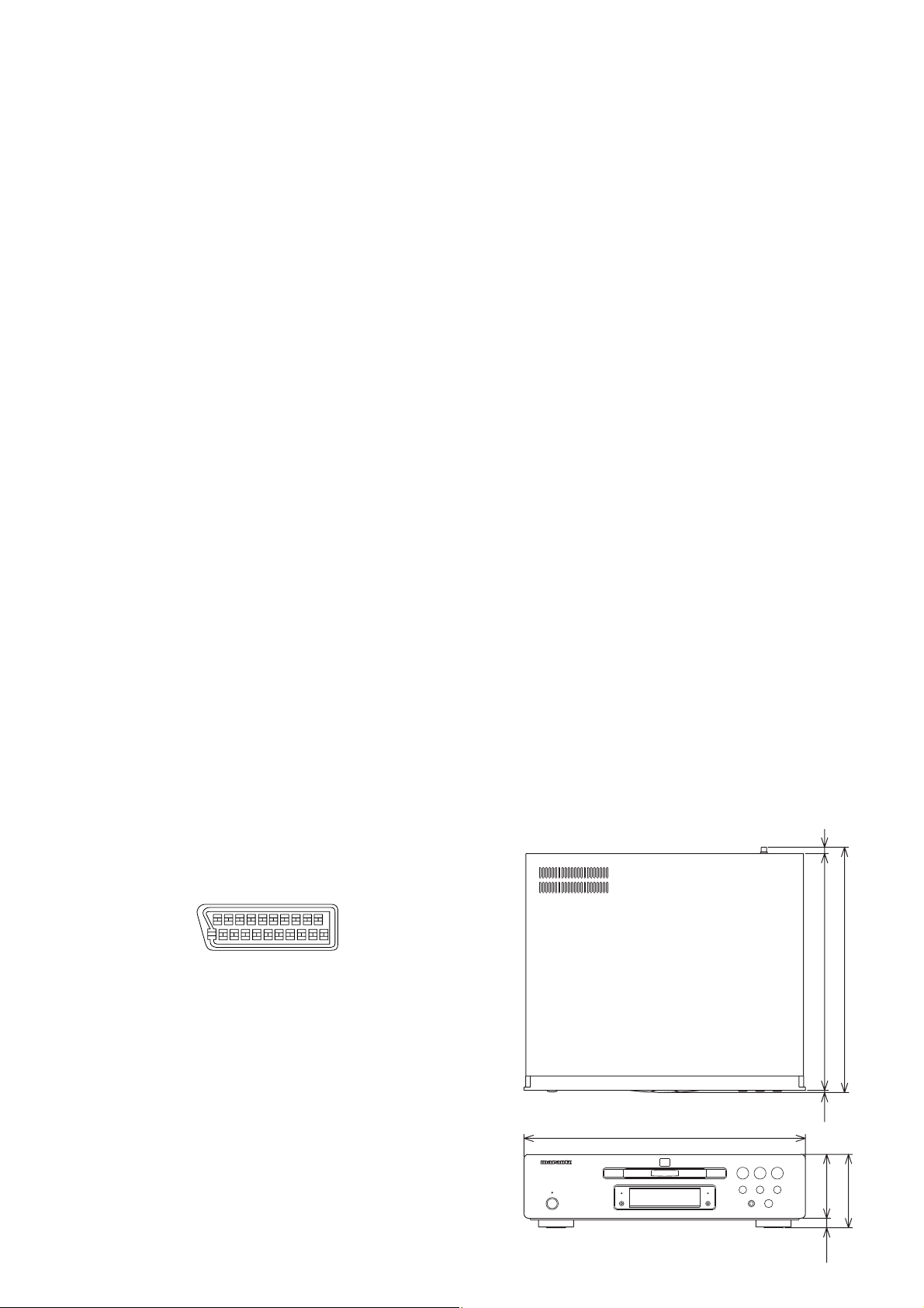
Dimensions......................... 440 (W) x 384 (D) x 115 (H) mm
(17.3 (W) x 15.1 (D) x 4.5 (H) in.)
(Not including protruding cables, etc.)
Operating temperature ... + 5 °C to + 35 °C (+ 41 °F to + 96 °F)
Operating humidity ................5 % to 85 % (no condensation)
S-Video output
Y (luminance) - Output level............................. 1 Vp-p (75 Ω)
C (color) - Output level : NTSC.................. 286 mVp-p (75 Ω)
: PAL ..................... 300 mVp-p (75 Ω)
Jacks ...............................................................S-VIDEO jack
Video output (2 individual outputs)
Output level....................................................... 1 Vp-p (75 Ω)
Jacks .......................................................................RCA jack
Component video output (Y, C
B/PB
, CR/PB)
Output level...............................................Y : 1.0 Vp-p (75 Ω)
C
B/PB
, CR/PR : 0.7 Vp-p (75 Ω)
Jacks .......................................................................RCA jack
HDMI output
Output Terminal ............................................................19-pin
21-pin connector assignment
AV connector output.................................... 21-pin connector
This connector provides the video and audio signals for
connection to a compatible color TV or monitor.
Audio output
Output level (During audio output).........2 Vrms (1 kHz, 0 dB)
Number of channels .............................................................2
Jacks .......................................................................RCA jack
Audio output (multi-channel / L, R, C, SW, LS, RS)
Output level (During audio output).........2 Vrms (1 kHz, 0 dB)
Number of channels .............................................................2
Jacks .......................................................................RCA jack
Digital audio characteristics
Frequency response............4 Hz to 44 kHz (DVD fs: 96 kHz)
4 Hz to 88 kHz (DVD-Audio fs: 192 kHz)
S/N ratio...................................................................... 130 dB
Dynamic range ........................................................... 110 dB
Total harmonic distortion .........................................0.0008 %
Wow and flutter.................................... Limit of measurement
(± 0.001 % W. PEAK) or lower
Digital output
Optical digital output..................................Optical digital jack
Coaxial digital output ...............................................RCA jack
i.LINK in/output
Output Terminal ..................................................4-pin (S400)
Other terminals
Control in/out ...........................................................RCA jack
Flasher input..................................................Mini jack (3.5Ø)
RS232C................................................................................1
Accessories
Audio/Video cable (yellow / red / white)................................1
System control cable ............................................................1
Power cable ..........................................................................1
Remote controller .................................................................1
AA (R6P) dry cell batteries ...................................................2
User guide ............................................................................1
2018161412108642
PIN no.
1 Audio 2/R out 11 G out
3 Audio 1/L out 15 R or C out
4 GND 17 GND
7 B out 19 Video out or Y out
8 Status 21 GND
21191715131197531
D1/D2 video output [except for N, U Version]
Output level...............................................Y : 1.0 Vp-p (75 Ω)
C
Jacks ..................................................................... D terminal
B/PB
, CR/PR : 0.7 Vp-p (75 Ω)
1
Page 4

Features
Equipped with an i.LINK port for
digital transfers of high-quality media
By simply connecting a single i.LINK cable
between components with i.LINK ports, you
can get direct digital transfers of not only
DVD-Video audio but also multi-channel
audio such as Super Audio CD or DVDAudio, which previously could only be
connected in analog with five audio cords, as
well as 2-channel audio like conventional
CDs (see page 55).
.
When transferring DVD-Audio or Super
Audio CD audio digitally by i.LINK, this unit
employs the Jitter Free Transfer System
(JFTS), a technology that removes jitter from
transfers. By combining this unit with JFTScompatible components, you can play jitterfree audio.
An HDCP-compatible HDMI*1 terminal
is provided to ensure the very highest
picture and digital sound quality by
fully digital transmission.
This unit comes with a High-Definition
Multimedia Interface (HDMI) jack, an
extended DVI interface for next-generation
televisions. This interface allows transfers of
uncompressed digital video and digital audio
(audio streams like Dolby Digital and DTS as
well as linear PCM) with a single connector.
HDMI standard Ver. 1.1 compatibility means
the unit can also transfer DVD-Audio multichannel audio over HDMI.
End-to-end full-digital transfers with alldigital processing make it possible to enjoy
realistic video without any of the image
degradation from AD/DA conversions. And
with the inclusion of our newly developed,
high-precision 10-bit scaler IC, the unit can
up-convert 480p video signals to 720p,
1080i, and 1080p video output signals by
way of the scaling function and the HDMI
jack (see page 52).
.
to let you enjoy beautiful video possible
with DVD. Furthermore, NSV technology
suppresses noise during DA conversion.
Support for 10-bit advanced
progressive NTSC/PAL with newly
developed chroma-error
compensation.
Our newly developed chroma-error compensation completely eliminates the chroma
error that occurs near perpendicular edges
in color-difference signals.
dts 96kHz/24 bit compatibility
It is equipped with a dts 96/24 decoder
that lets you enjoy dts audio with sound
quality as high as 96kHz/24bit. This product does not support dts 88.2kHz/24bit.
Dolby Headphone compatibility
The Head Phone can reproduce the world of
Dolby Surround with realistic ambience like
that you would experience using a 5.1 ch
system (Excluding Super Audio CD) (see
page 13).
.
Lip Sync capability
When it is connected to a plasma display or
projector, it corrects the time lag between
the video and audio created by the video
circuit processing time in units of 10msec up
to a maximum of 200msec. It precisely
synchronizes the actors’ voices and the
movements of their mouths (see page 31).
.
Equipped with a Super Audio CD
Distance compensation function
It can perform Distance adjustment of Super
Audio CD that was formerly impossible by
converting it to PCM (see page 44).
.
Superlative audio performance with
Super Audio CD, DVD-Audio, Dolby*
3
Digital and DTS*4 software
Logos:
High quality 14-bit/216MHz Video D/
A converter*
The unit uses a Video D/A converter that
performs D/A conversion of all video signals
in 14-bits and can perform 8X over-sampling
2
The DV9600 delivers breathtaking sound
quality with Super Audio CD, DVD-Audio,
Dolby Digital and DTS discs.
2
Page 5
Discs compatible with this player
Any disc that displays one of the following
logos should play in this player. Other
formats, including DVD-RAM, DVD-ROM,
DVD+RW, DVD+R, CD-ROM (except those
that contain MP3/JPEG files) and Photo CD
will not play.
DVD-Video compatibility:
• Logos:
• Single sided or double sided discs
• Single layer or dual layer discs
• Dolby Digital, DTS, MPEG or Linear PCM digital
audio
• MPEG-2 digital video
Discs are generally divided into one or more titles.
Titles may be further subdivided into chapters.
DVD-Audio compatibility:
• Logos:
• Single sided discs
• Single layer or dual layer discs
• Linear or packed PCM digital audio
• Some discs may contain MPEG-2 video, and
Dolby Digital, DTS or MPEG digital audio
Discs are generally divided into one or more
groups. Groups may be further subdivided into
tracks.
DVD-R compatibility:
This unit can play DVD-R discs. Please note the
following points when using these discs:
• Logo:
• This unit can play DVD-R discs recorded as
DVD-Video format.
• DVD-R discs that were recorded with copy-once
only permission cannot be played.
Capture
You can store a photograph of your children
as background (see page
.
29).
SRS TruSurround
*5
Logo:
When used with stereo sources, SRS
TruSurround creates a realistic surroundsound effect using just two speakers (see
page 44).
MP3 compatibility
This player is compatible with CD-R, CD-RW
and CD-ROM discs that contain MP3 audio
tracks (see pages 9, 28).
.
JPEG compatibility
This player is compatible with CD-R, CD-RW
and CD-ROM discs that contain JPEG data
(see pages 9, 29).
*1HDMI, the HDMI logo and High-Definition
Multimedia Interface are trademarks or registered trademarks of HDMI Licensing LLC.
*2“NSV” is a registered trademark of Analog
Device Co. Ltd.
*3Manufactured under license from Dolby
Laboratories. “Dolby” and the double-D symbol
are trademarks of Dolby Laboratories. Confidential unpublished works. © 1992-1997 Dolby
Laboratories. All rights reserved.
4
“DTS” and “DTS 96/24” are trademarks of
*
Digital Theater Systems, Inc.
5
*
TruSurround, SRS and the
trademarks of SRS Labs, Inc. TruSurround
technology is incorporated under license from
SRS Labs, Inc.
.
®
symbol are
.
3
Page 6
DVD-RW compatibility:
DVD-Video regions
All DVD-Video discs carry a region mark on
the case somewhere that indicates which
region(s) of the world the disc is compatible
with. Your DVD player also has a region
mark, which you can find on the rear panel.
Discs from incompatible regions will not play
in this player. Discs marked ALL will play in
any player.
MP3 compatibility information
• The CD-ROM must be ISO 9660 compatible.
• Files should be MPEG1 Audio Layer 3 format,
44.1kHz or 48kHz. Incompatible files will not
play.
• This player is not compatible with MP3 PRO,
ID3-Tag and packet write.
• When using a variable bit rate, files may be
played back at speeds between 32Kbps and
320Kbps.
• This player cannot play DVD-R/RW discs with
recorded MP3 music data.
• VBR files may not show play times correctly.
• This player only plays tracks that are named
with the file extension “.mp3” or “.MP3”.
• This player is not compatible with multi-session
discs. If you try and play a multi-session disc,
only the first session will be played.
• Use CD-R or CD-RW media for recording your
MP3 files. The disc must be finalized in order to
play.
• Audio encoded at 128Kbps should sound close
to regular audio CD quality. Although this
player will play lower bit-rate MP3 tracks, the
sound quality becomes noticeably worse at
lower bit-rates.
• Only the first 8 characters of folder and track
names (excluding the “.mp3” extension) are
displayed.
• This player can recognize about total 600 files/
folder.
This unit can play DVD-RW discs. Please note the
following points when using these discs:
• Logo:
• This unit can play DVD-RW discs recorded as
DVD-Video format.
• DVD-RW discs that were recorded with copyonce only permission cannot be played.
Audio CD compatibility:
• Logos:
• 12cm (5in.) or 8cm (3in.) discs
• Linear PCM digital audio
• Audio CD, CD-R* and CD-RW* formats
CDs are divided into tracks.
*This unit can play CD-R and CD-RW discs
recorded in Audio CD or Video CD format, or with
MP3 audio files.
*Some copy-controlled CDs may not conform to
official CD standards. They are special discs and
may not play on the DV9600.
*The audio side of dual discs does not conform to
CD standards and may not play on the DV9600.
Video CD compatibility:
• Logo:
• 12cm (5in.) or 8cm (3in.) discs
• MPEG-1 digital audio
• MPEG-1 digital video
Video CDs are divided into tracks.
Super VCD compatibility:
• Logo:
• 12cm (5in.) or 8cm (3in.) discs
• MPEG-1 digital audio
• MPEG-2 digital video
Super VCDs are divided into tracks.
Super Audio CD compatibility:
• Logo:
• Single layer, dual layer or Hyblid layer
• 12cm (5in.) or 8cm (3in.) discs
• Digital audio (DSD)
Super Audio CDs are divided into tracks.
4
Page 7

JPEG compatibility information
• While this player is designed to be able to
handle image data recorded in JPEG format, no
assurances are given that the player will be able
to display image data recorded in all JPEG
formats.
• Display is limited to the display of files up to
30MB in size.
• This player cannot display progressive JPEG
images.
• When writing JPEG files to CD-R/RW discs,
always be sure to set the writing format to ISO
9660 Level 1.
• Always be sure to specify a file extension of
“.JPG” or “.JPE” for JPEG files. The file will not be
able to be displayed if a file extension other
than “.JPG” or “.JPE” is specified or if no file
extension is assigned to the file. (Note that this
means that JPEG files created on a Macintosh
will not be able to be displayed as is.)
Caution!
• DVD-R/RW and CD-R/RW discs recorded using
a personal computer or a DVD or CD recorder
may not play if the disc is damaged or dirty, or
if there is dirt or condensation on the player’s
lens.
• If you record a disc using a personal computer,
even if it is recorded in a compatible format,
there are cases in which it may not play because
of the settings of the application software used
to create the disc. (Check with the software
publisher for more detailed information.)
• Unfinalized DVD-R/RW discs cannot be played.
• Unfinalized CD-R/RW discs cannot be played.
• For more information on using DVD-R/RW and
CD-R/RW discs, see “Handling discs” on page
60.
• Never try to replay anything other than a music
CD (CDA format) or a CD-R/RW on which MP3
and/or JPEG files have been stored. Depending
on the type of file, there may be times when
doing so will result in problems or erroneous
operation.
• There may be times when it is impossible to
replay a CD-R/RW disc because of the characteristics of the disc being used or because of
dirt or scratches on the disc.
.
5
Page 8
2. SERVICE HINTS AND TOOLS
SERVICE HINTS
SERVICE TOOLS
Audio signals disc 4822 397 30184
Disc without errors (SBC444)+
Disc with DO errors, black spots and fingerprints (SBC444A) 4822 397 30245
Disc (65 min 1kHz) without no pause 4822 397 30155
Max. diameter disc (58.0 mm) 4822 397 60141
Torx screwdrivers
Set (straight) 4822 395 50145
Set (square) 4822 395 50132
13th order filter 4822 395 30204
DVD test disc (PAL) 4822 397 10131
DVD test disc (NTSC) ALMEDIO TDV-540
6
Page 9
3. WARNING AND LASER SAFETY INSTRUCTIONS
GB
WARNING
All ICs and many other semi-conductors are
susceptible to electrostatic discharges (ESD).
Careless handling during repair can reduce
life drastically.
When repairing, make sure that you are
connected with the same potential as the
mass of the set via a wrist wrap with
resistance.
Keep components and tools also at this
potential.
F
ATTENTION
D
WARNUNG
I
WAARSCHUWING
AVVERTIMENTO
NL
Alle IC’s en vele andere halfgeleiders zijn
gevoelig voor elektrostatische ontladingen
(ESD).
Onzorgvuldig behandelen tijdens reparatie
kan de levensduur drastisch doen
verminderen.
Zorg ervoor dat u tijdens reparatie via een
polsband met weerstand verbonden bent met
hetzelfde potentiaal als de massa van het
apparaat.
Houd componenten en hulpmiddelen ook op
ditzelfde potentiaal.
Tous les IC et beaucoup d’autres semiconducteurs sont sensibles aux décharges
statiques (ESD).
Leur longévité pourrait être considérablement
écourtée par le fait qu’aucune précaution
n’est prise a leur manipulation.
Lors de réparations, s’assurer de bien être
relié au même potentiel que la masse de
l’appareil et enfiler le bracelet serti d’une
résistance de sécurité.
Veiller a ce que les composants ainsi que les
outils que l’on utilise soient également a ce
potentiel.
GB
Safety regulations require that the set be restored to its original condition
and that parts which are identical with those specified be used.
NL
Veiligheidsbepalingen vereisen, dat het apparaat in zijn oorspronkelijke
toestand wordt terug gebracht en dat onderdelen, identiek aan de
gespecifieerde worden toegepast.
Alle IC und viele andere Halbleiter sind
empfindlich gegen elektrostatische
Entladungen (ESD).
Unsorgfältige Behandlung bei der Reparatur
kann die Lebensdauer drastisch vermindern.
Sorgen sie dafür, das Sie im Reparaturfall
über ein Pulsarmband mit Widerstand mit
dem Massepotential des Gerätes verbunden
sind.
Halten Sie Bauteile und Hilfsmittel ebenfalls
auf diesem Potential.
D
Bei jeder Reparatur sind die geltenden Sicherheitsvorschriften zu beachten.
Der Originalzustand des Gerats darf nicht verandert werden.
Fur Reparaturen sind Original-Ersatzteile zu verwenden.
I
Le norme di sicurezza esigono che l’apparecchio venga rimesso nelle
condizioni originali e che siano utilizzati pezzi di ricambiago idetici a quelli
specificati.
Tutti IC e parecchi semi-conduttori sono
sensibili alle scariche statiche (ESD).
La loro longevita potrebbe essere fortemente
ridatta in caso di non osservazione della piu
grande cauzione alla loro manipolazione.
Durante le riparazioni occorre quindi essere
collegato allo stesso potenziale che quello
della massa dell’apparecchio tramite un
braccialetto a resistenza.
Assicurarsi che i componenti e anche gli
utensili con quali si lavora siano anche a
questo potenziale.
F
“Pour votre sécurité, ces documents
doivent être utilisés par des
spécialistes agrées, seuls habilités à
réparer votre appareil en panne.”
Les normes de sécurité exigent que l’appareil soit remis a l’état d’origine et
que soient utilisées les pièces de rechange identiques à celles spécifiées.
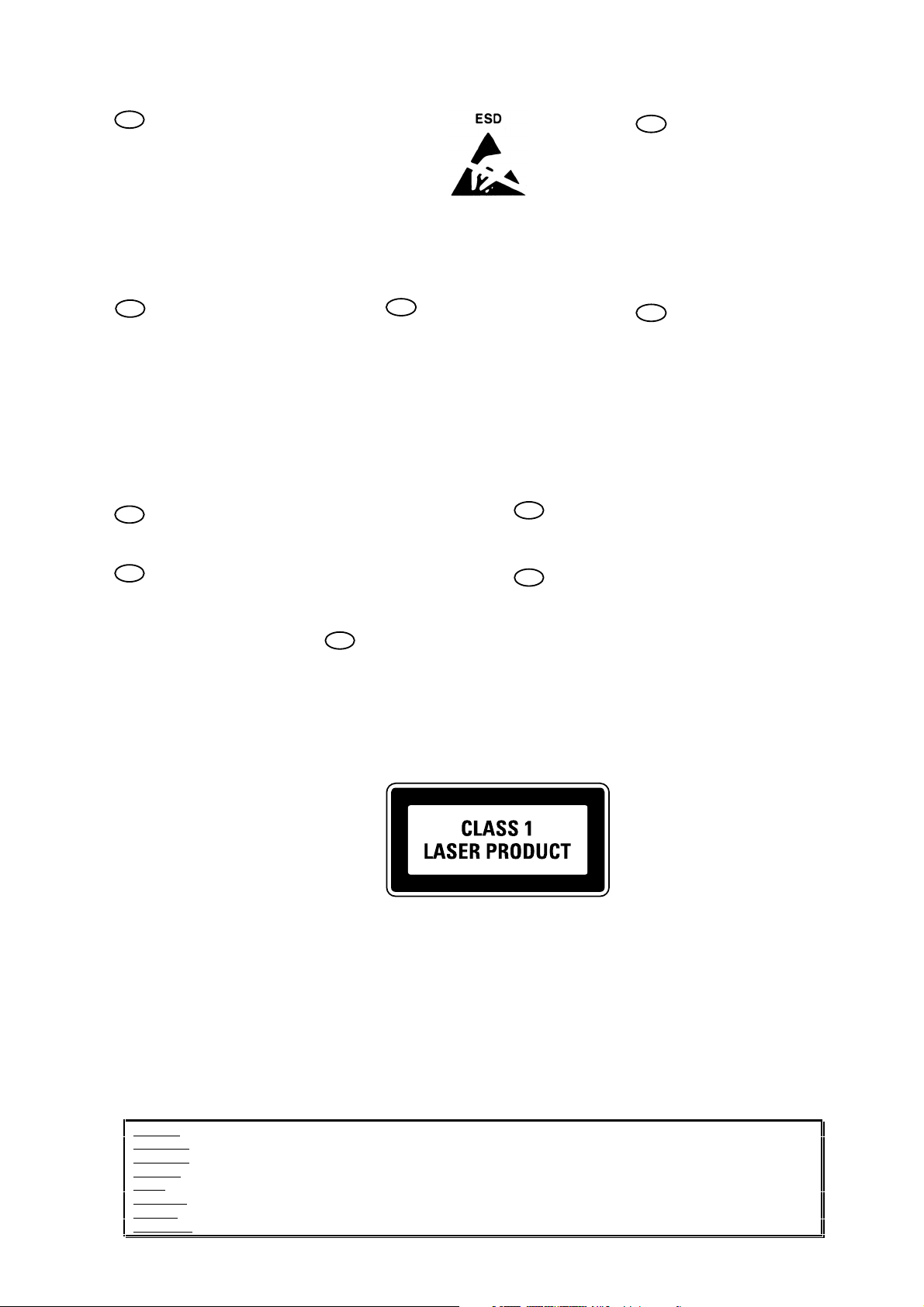
LASER SAFETY
This unit employs a laser. Only a qualified service person should remove the cover or attempt to service this
device, due to possible eye injury.
USE OF CONTROLS OR ADJUSTMENTS OR PERFORMANCE OF PROCEDURE OTHER THAN THOSE
SPECIFIED HEREIN MAY RESULT IN HAZARDOUS RADIATION EXPOSURE.
AVOID DIRECT EXPOSURE TO BEAM
WARNING
The use of optical instruments with this product will increase eye hazard.
Repair handling should take place as much as possible with a disc loaded inside the player
WARNING LOCATION: INSIDE ON LASER COVERSHIELD
CAUTION VISIBLE AND INVISIBLE LASER RADIATION WHEN OPEN AVOID EXPOSURE TO BEAM
ADVARSEL SYNLIG OG USYNLIG LASERSTRÅLING VED ÅBNING UNDGÅ UDS
ADVARSEL SYNLIG OG USYNLIG LASERSTRÅLING NÅR DEKSEL Å PNES UNNGÅ EKSPONERING FOR STRÅLEN
VARNING SYNLIG OCH OSYNLIG LASERSTRÅLNING NÄR DENNA DEL ÄR ÖPPNAD BETRAKTA EJ STRÅLEN
VARO! AVATT AESSA OLET ALTTIINA NÄKYVÄLLE JA NÄKYMÄTTÖMÄLLE LASER SÄTEILYLLE. ÄLÄ KATSO SÄTEESEEN
VORSICHT SICHTBARE UND UNSICHTBARE LASERSTRAHLUNG WENN ABDECKUNG GEÖFFNET NICHT DEM STRAHL AUSSETSEN
DANGER VISIBLE AND INVISIBLE LASER RADIATION WHEN OPEN AVOID DIRECT EXPOSURE TO BEAM
ATTENTION RAYONNEMENT LASER VISIBLE ET INVISIBLE EN CAS D'OUVERTURE EXPOSITION DANGEREUSE AU FAISCEAU
Æ
TTELSE FOR STRÅLING
030804ecm
7
Page 10
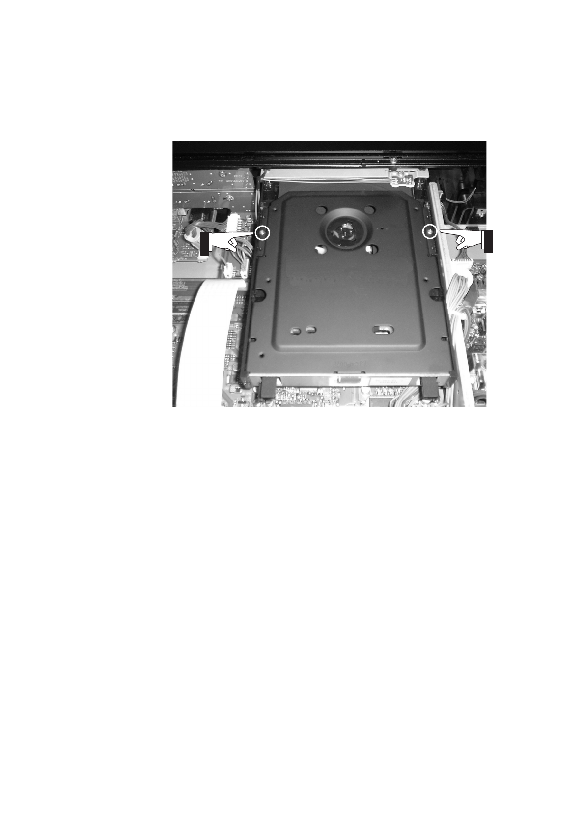
4. TAKING THE DISC OUT OF EMERGENCY
1. Remove the top cover of the player.
2. Remove 2 screws shown in the picture follows.
3. Remove the disc clamper.
4. Now you can remove the disc.
Remove those screws
8
Page 11

5. UPDATE BACK END SOFTWARE
(FIRMWARE) PROCEDURE
5. Back End Software(Firmware)の
書き換え方法
Necessary Equipment
• Update Disc (for Back End Software).
1. Press POWER button, and turn on the DVD Play er.
2. Press Open/Close button, and open the tray.
3. The update disc is placed on the tray.
4. Press Open/Close button, and close the tray.
5. After Loading the Disc, the front display shows "VCD"
for a moment. Next, the front dis play shows "WRITNG",
And Back End Software is updated au to mat i cal ly.
6. At this time, "Updating Flash Memory" shows on the
mon i tor.
7. The tray will be opened, when finished updating
software.
8. At this time, after the front dis play shows "VCD" for a
mo ment, it shows "COMPLETE".
9. Take out the update disc from the tray.
10. Press the Open/Close button, and close the tray.
11. Press the POWER button, and turn off the DVD Player.
必要機器
• Back End Software のアップデート用 CD-ROM
1. POWER
2. Open/Close ボタンを押し、トレーを出します。
3. Back End Software のアップデートディスクをトレーに乗
せます。
4. Open/Close ボタンを押し、トレーを戻します。
5. Disc の Loading を行った後フロントディスプレイに
"VCD" と一瞬表示し、"WRITING" と表示され Soft ware
のアップデートは自動で行われます。
6. TV またはモニターの OSD には "Updating Flash
Memory"
7. アップデートが終わるとトレーが自動で開きます。
8. フロントディスプレイに一瞬 "VCD" と表示された後、
"COMPLETE" と表示されます。
9. アップデートディスクを取り出します。
10. Open/Close を押し、トレーを閉じます。
11. POWER ボタンを押し、電源を切ります。
ボタンを押し、DVD Player の電源を入れます。
と表示されます。
9
Page 12
6. UPDATE PANEL MICROPROCESSOR
PROCEDURE
Necessary Equipment
• Windows PC (OS: Windows2000 or WindowsXP) with
Serial Port
• RS-232C Cable straight type (9 Pin female - 9 Pin
female)
• Update Tool: FDTsetup.EXE(FDT3.0) or
fdtv30300.exe(FDT3.3)
• Update data (CSIDE_vxxx.mot)
NOTE: File name will change according to release date.
Update of PANEL Microprocessor can be updated by
FDT3.0 or FDT3.3.
Supposing you already installed FDT3.0 or FDT3.3, move
on to the Writing software setup procedure.
If you do not have FDT, move on to the Download and
install updating software for Microprocessor.
6. PANEL MICROPROCESSOR の書き換え方法
必要機器
• Windows PC Serial Port 付き (OS: Windows2000 または
WindowsXP)
• RS-232C
書き込み用アプリケーションツール (FDTsetup.EXE
•
(FDT3.0)
書き込み用データ (CSIDE_vxxx.mot)
•
NOTE: xx
パネルマイコンのアップデートは
アップデートすることが出来ます。
既に
FDT3.0 または FDT3.3 をインストールしてある場合は書
き込みソフトウェアの設定に進んでください。
もし、
ダウンロードとインストール手順に進んでください。
ストレートケーブル (9Pin メス− 9Pin メス )
または fdtv30300.exe(FDT3.3))
は改版番号です。
FDT3.0 でも FDT3.3 でも
FDT を持っていない時は、アップデートソフトウェアの
Panel Microprocessor Update Procedure
1. DOWNLOADS OF THE SOFTWARE
Download the software for update of the PANEL
microprocessor.
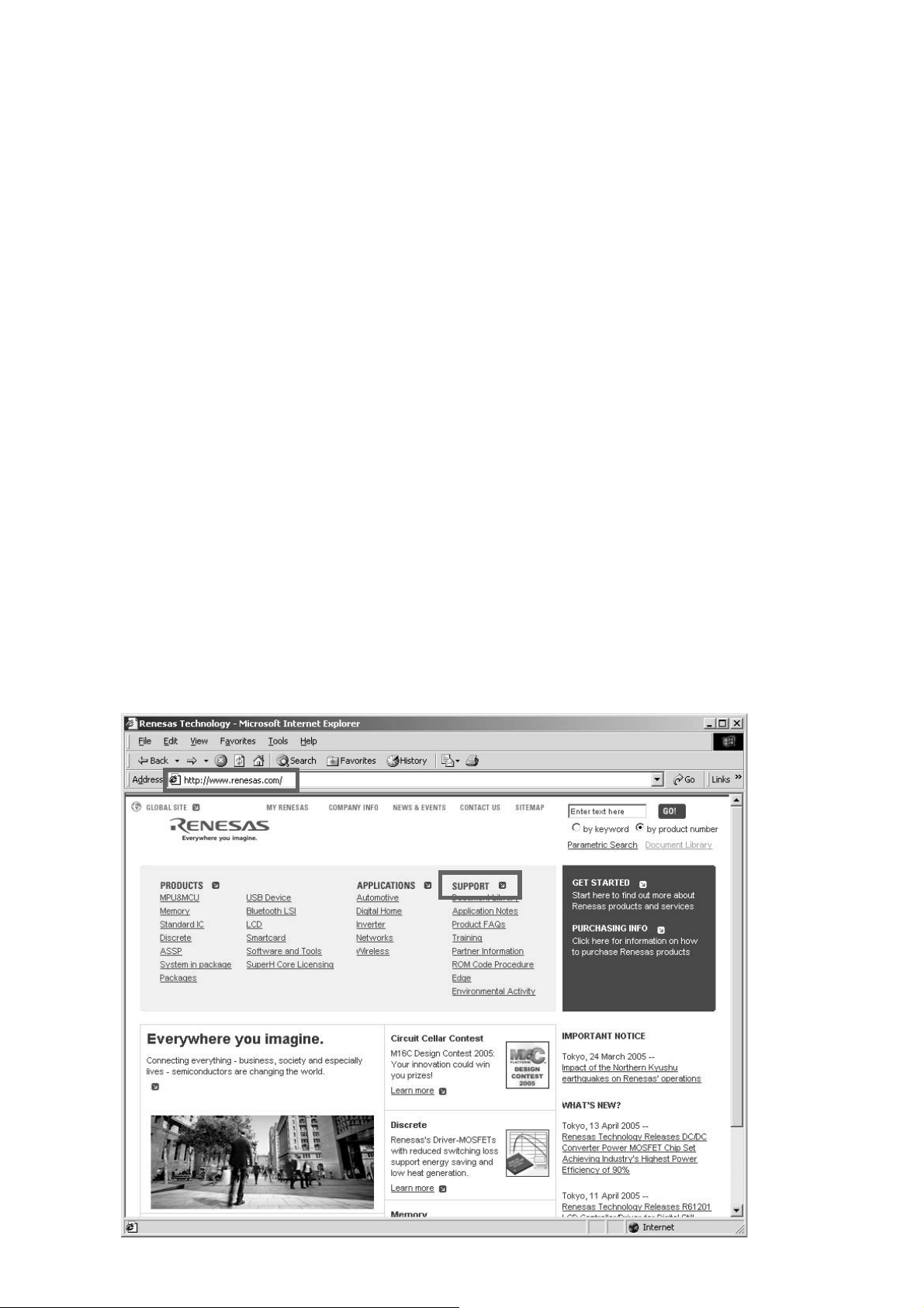
Launch up the browser. Type http://www.renesas.com/ into
an address. And press Enter.
(When site of Renesas is modified, please search "Flash
Development Toolkit", or type http://download.renesas.com/e
ng/mpumcu/index.html into an address.)
Click the SUPORT on the site of Renesas.
書き込み手順
1. DOWNLOADS OF THE SOFTWARE
PA NE L
ドします。
Browser を起動し、Address へ http://www.renesas.com/ と入
力し、
(Renasas
Toolkit
com/eng/mpumcu/index.html
Renesas
SUPPORT
マイコンのアップデート用ソフトウェアをダウンロー
Enter を押します。
のサイトが変更になった場合は、
を検索するか、
のホームページが開きますので、ここから
をクリックします。
Addressへhttp://download.renesas.
を入力してください。
Flash Development
)
10
Page 13
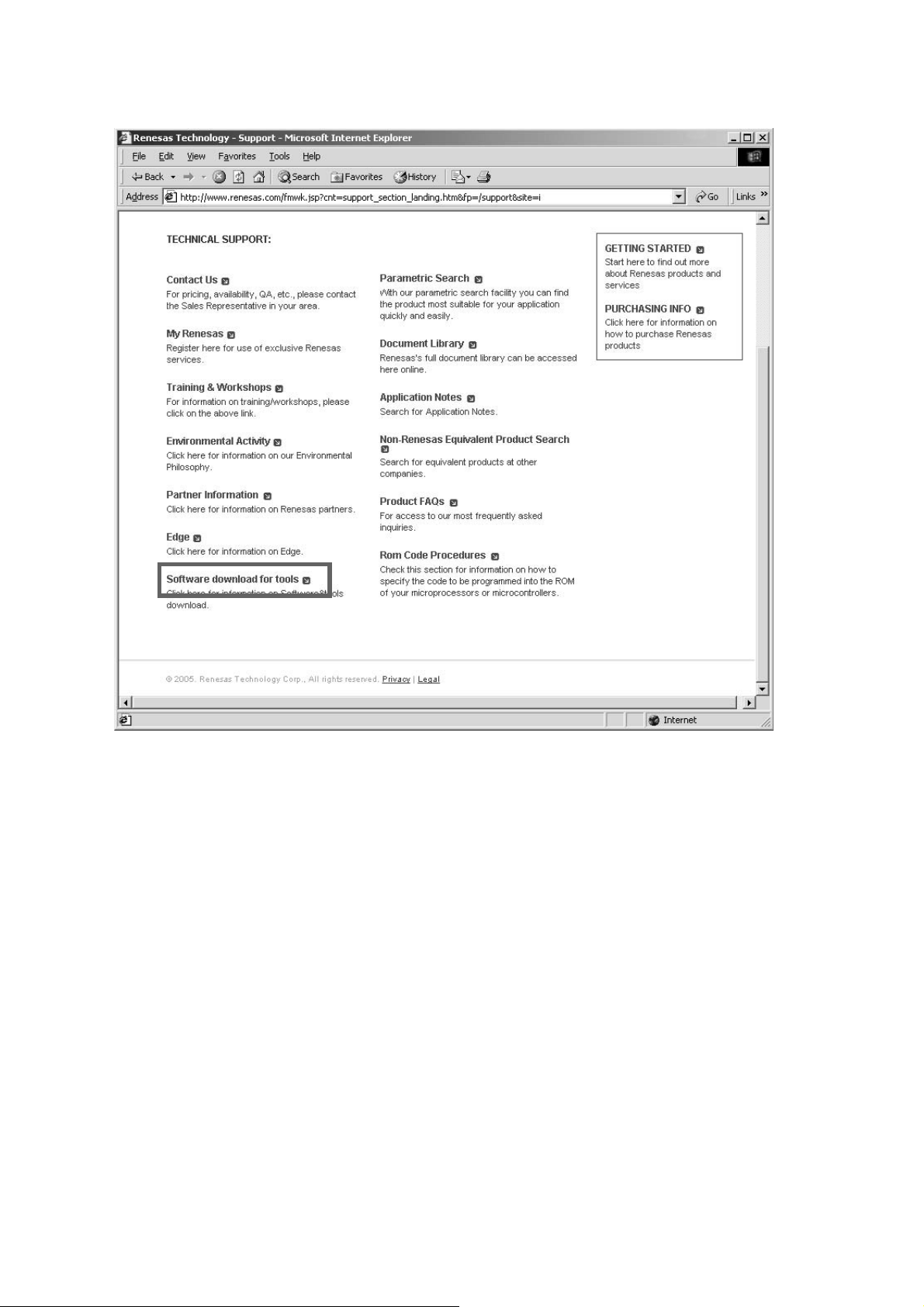
Click the Software download for tools on Support.
Support のページから Software download for tools をクリ
ックします。
11
Page 14
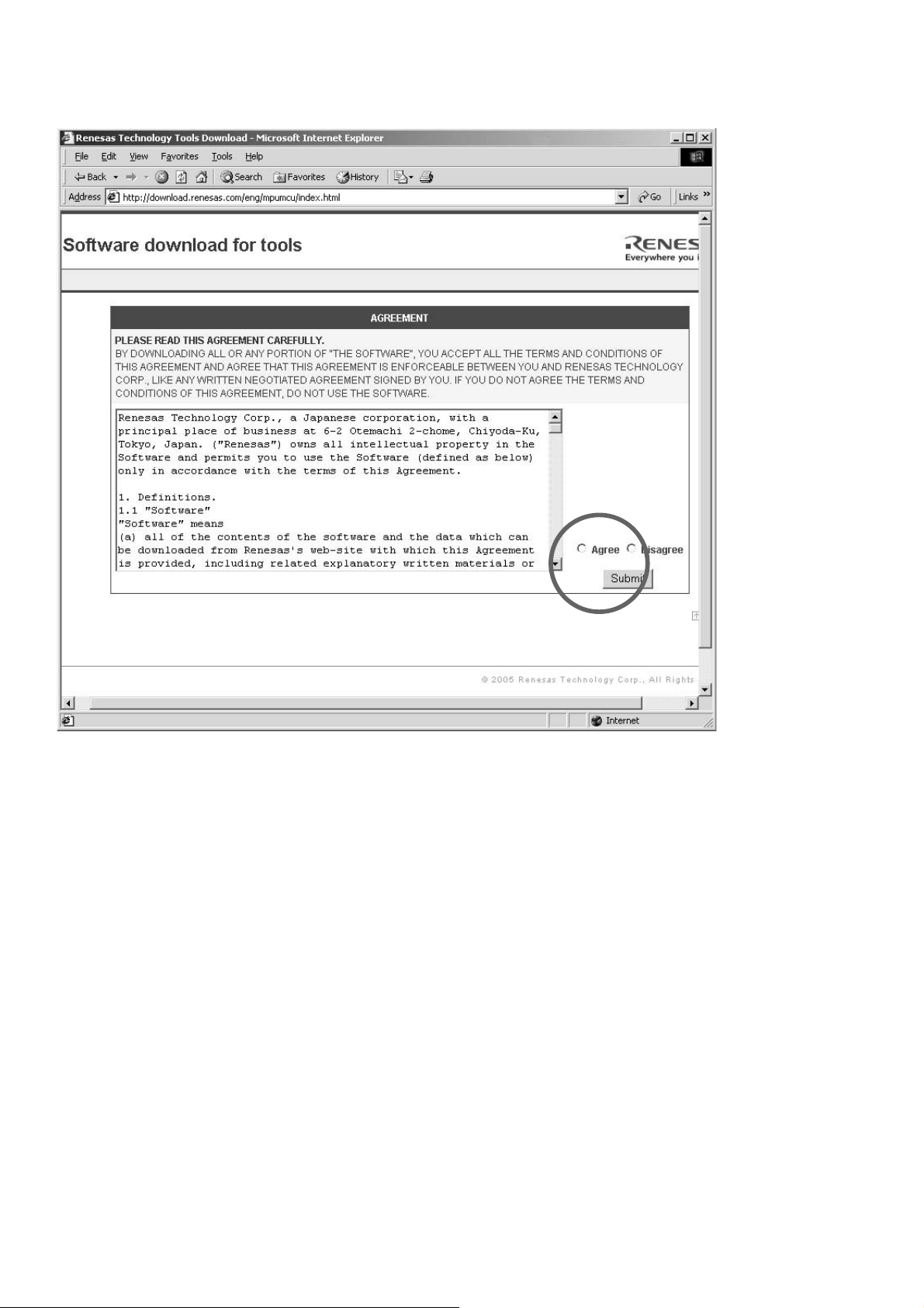
Check the Agree on AGREEMENT. And click Submit.
AGREEMENT から Agree にチェックを入れ Submit をクリ
ックします。
12
Page 15
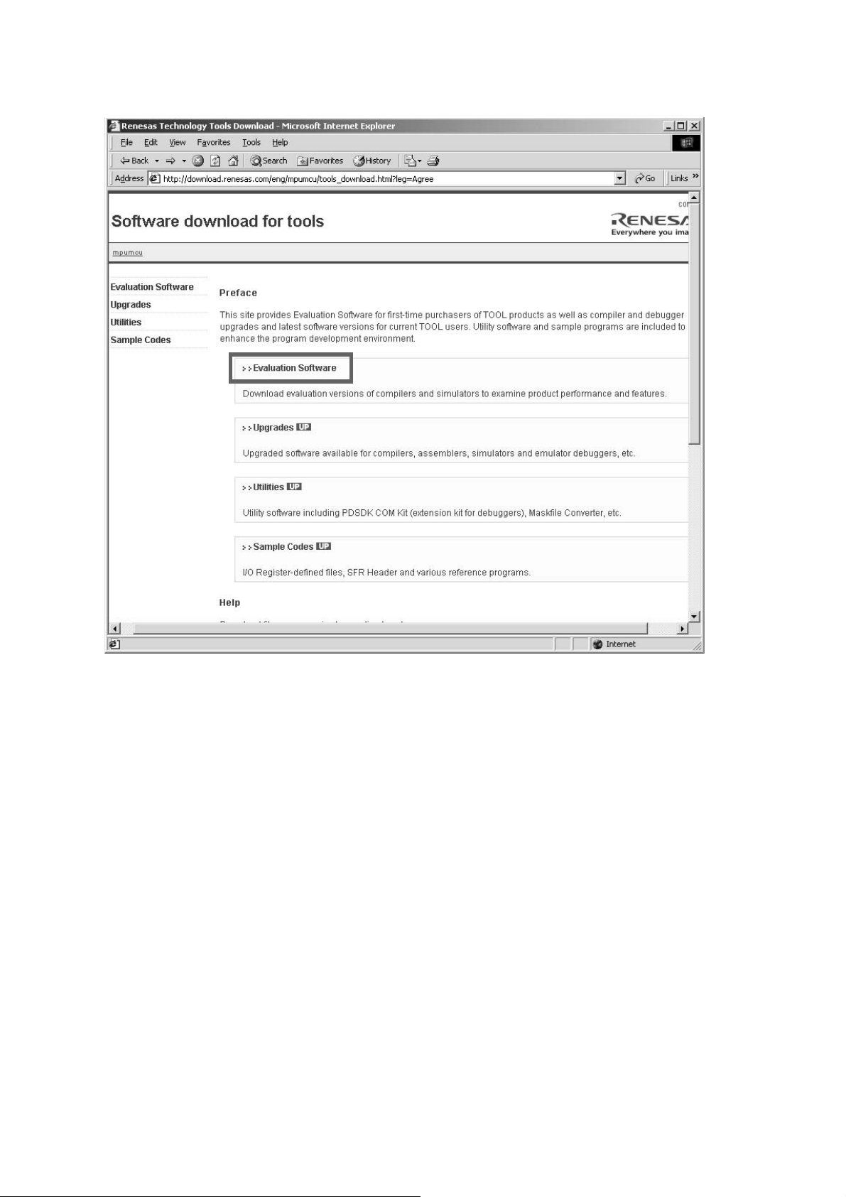
Click Evaluation Software.
Evaluation Software をクリックします。
13
Page 16
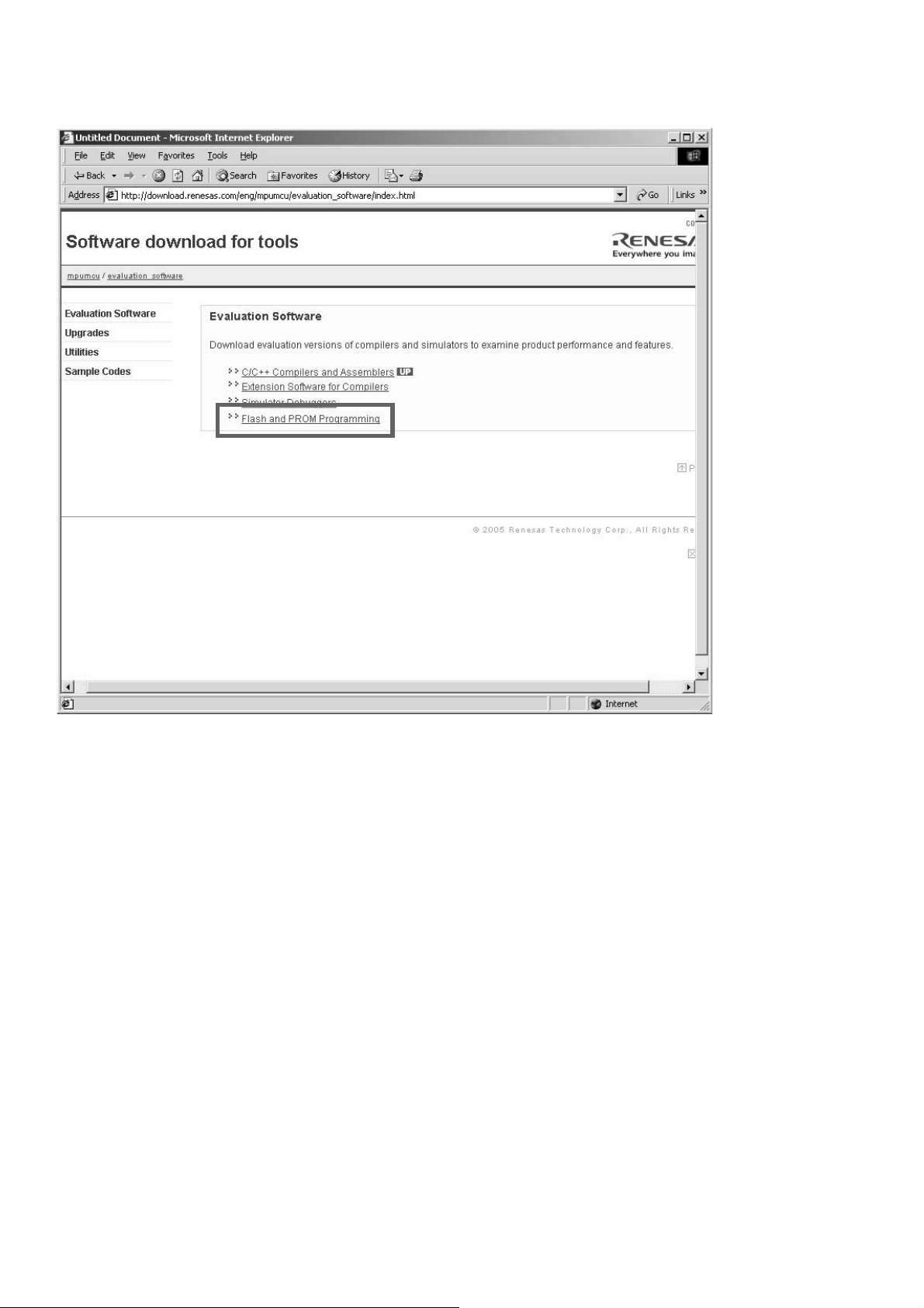
Click Flash and PROM Programming.
Flash and PROM Programming をクリックします。
14
Page 17
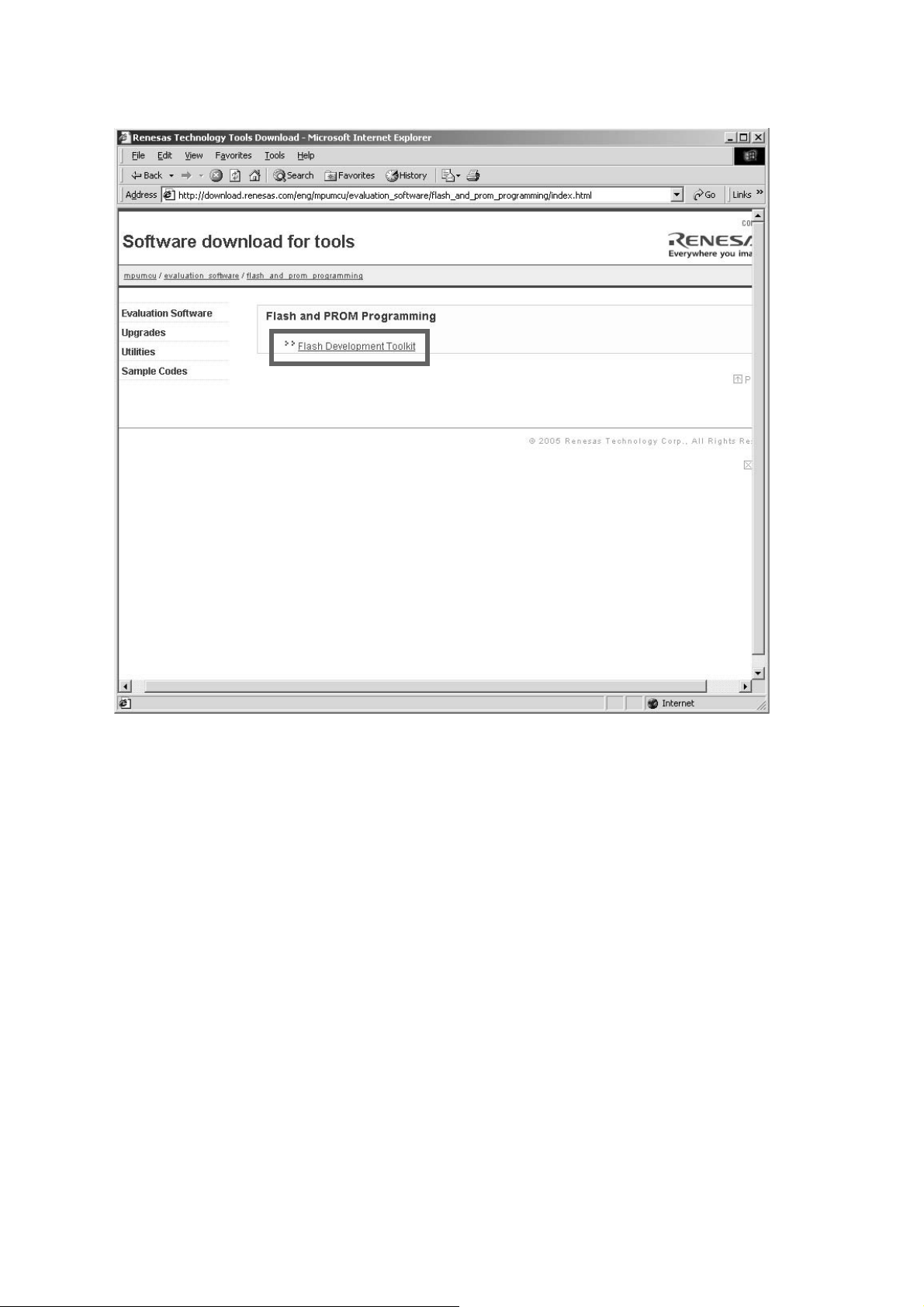
Click Flash Development Toolkit.
Flash Development Toolkit をクリックします。
15
Page 18
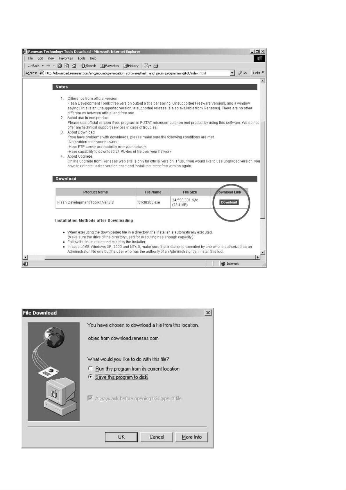
Click Download.
Page Down をし、Download をクリックします。
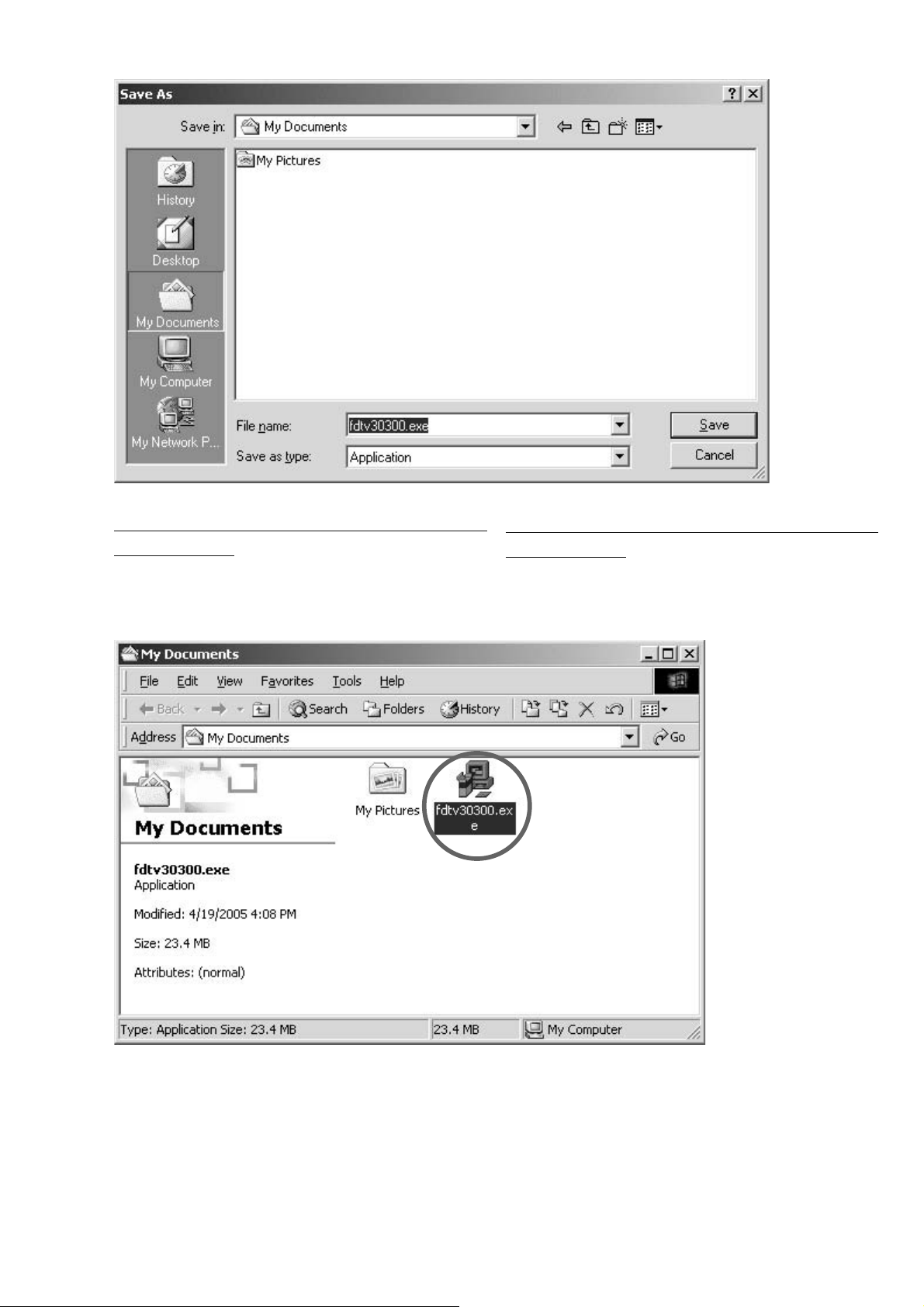
Save the fdtv30300.exe on your PC’s hard disc.
(A file name is changed by improvement.)
fdtv30300.exe を任意のフォルダに保存します。
( ファイル名はヴァージョンアップにより変更になる場合があ
ります。
)
16
Page 19
INSTALLS OF THE SOFTWARE (FLASH DEVELOPMENT
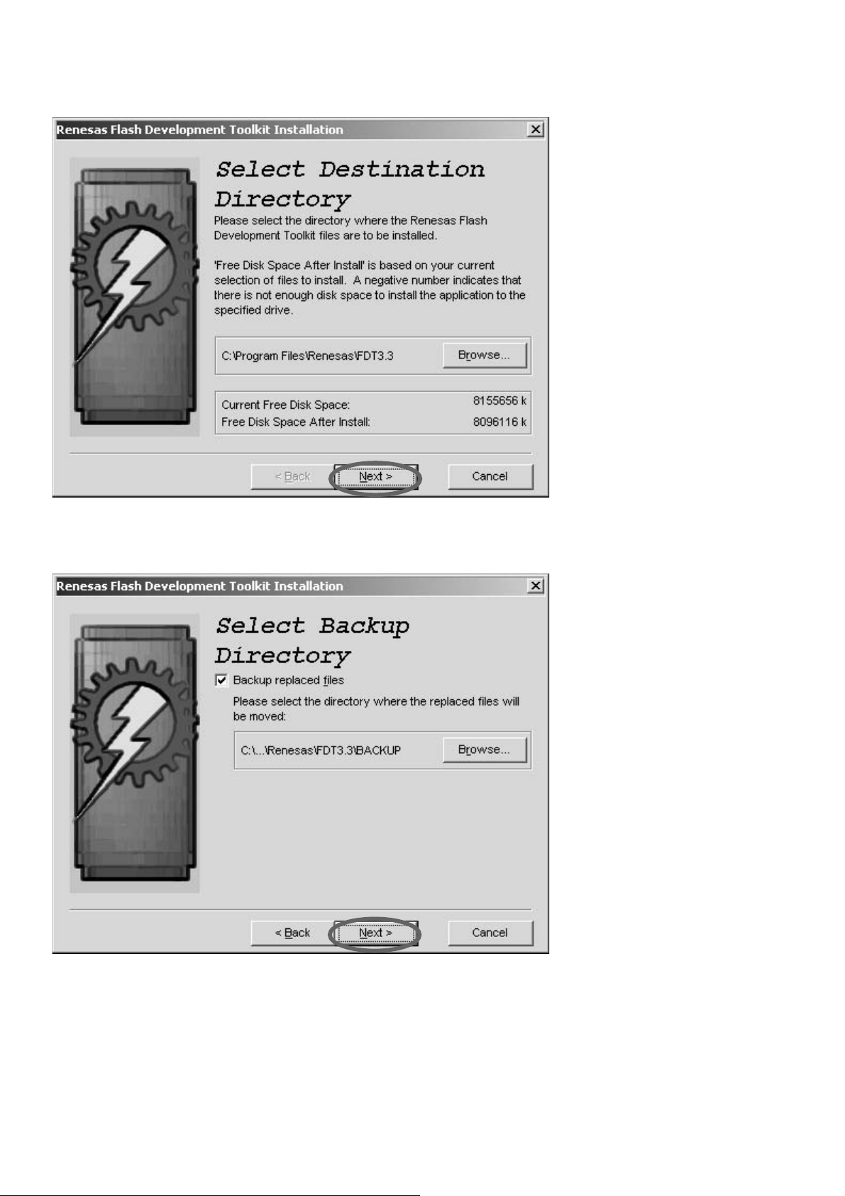
TOOLKIT VER.3.3)
Open the folder with the downloaded file. And double click
the fdtv30300.exe.
INSTALLS OF THE SOFTWARE (FLASH DEVELOPMENT
TOOLKIT VER.3.3)
ダウンロードしたファイルを保存しているフォルダを開きま
す。
fdtv30300.exe ファイルをダブルクリックします。
17
Page 20
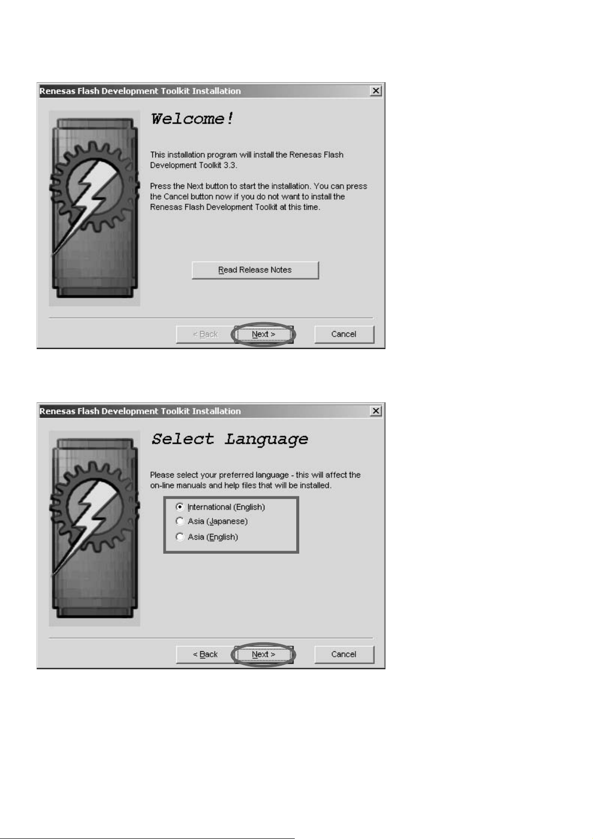
Click Next >.
Next > をクリックします。
Choose the language. And click Next >.
言語を選んで
Next > をクリックします。
18
Page 21
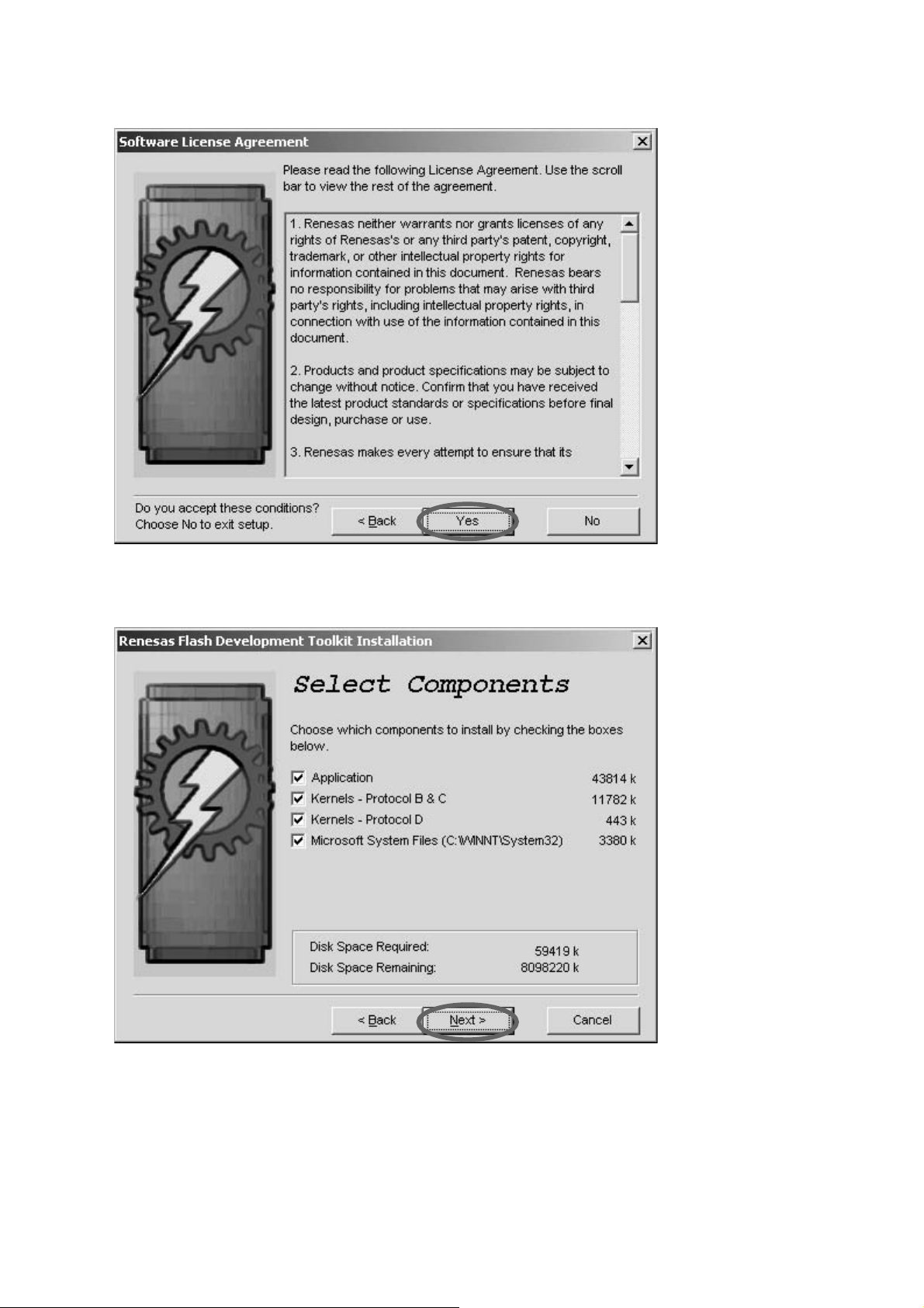
Click Yes .
Yes をクリックします。
Click Next >.
Next > をクリックします。
19
Page 22
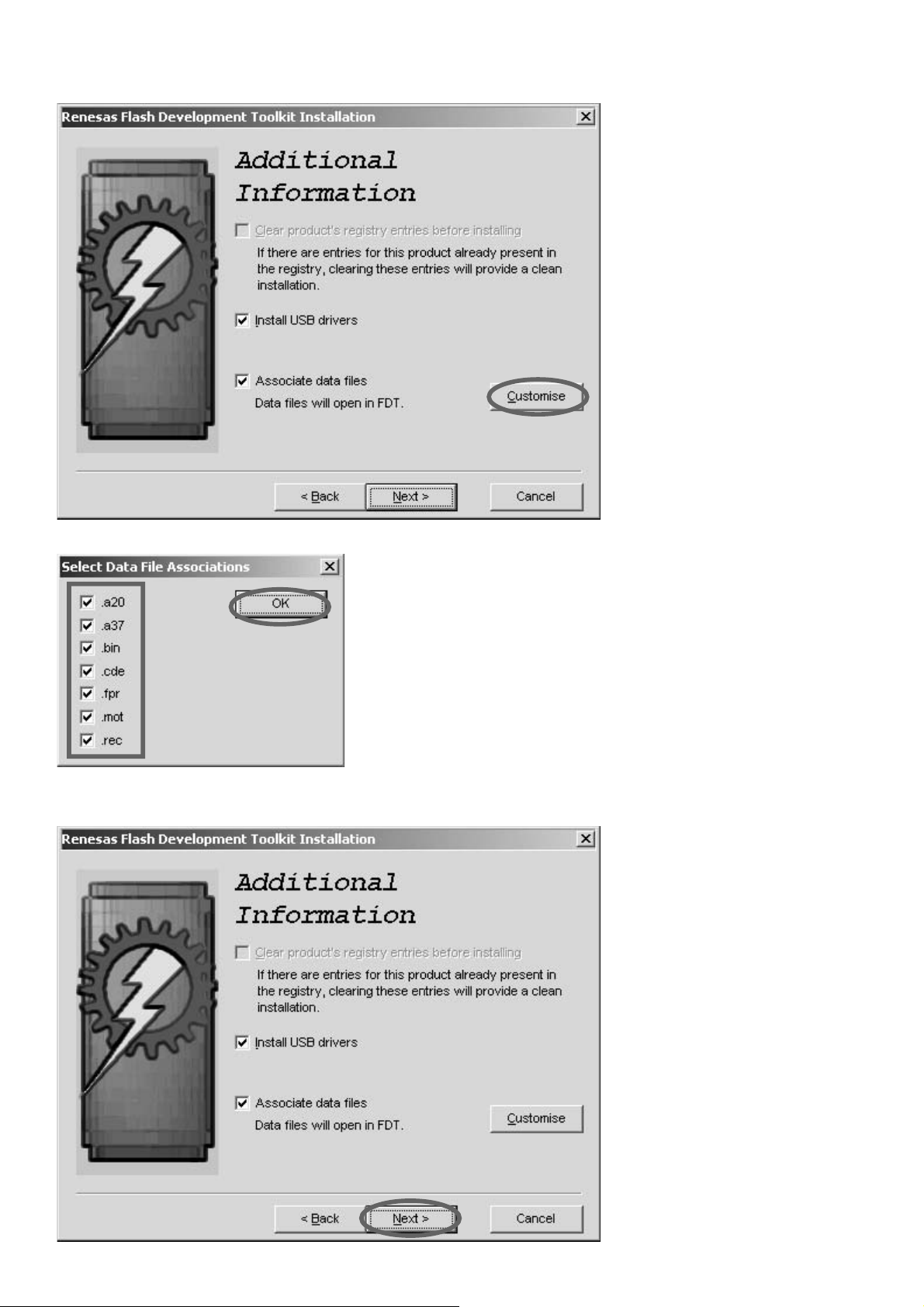
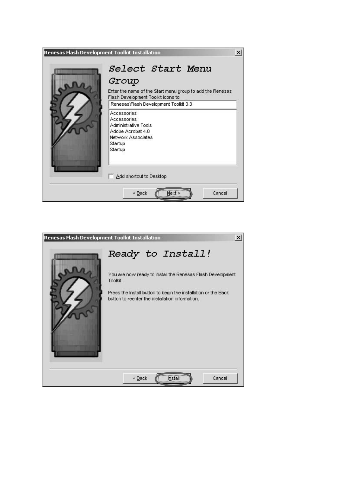
Click Customise.
Customise をクリックします。
Check to the all check box. And click OK.
Click Next >.
全てのチェックボックスにチェックが入っていることを確認
し、
OK をクリックします。
Next > をクリックします。
20
Page 23
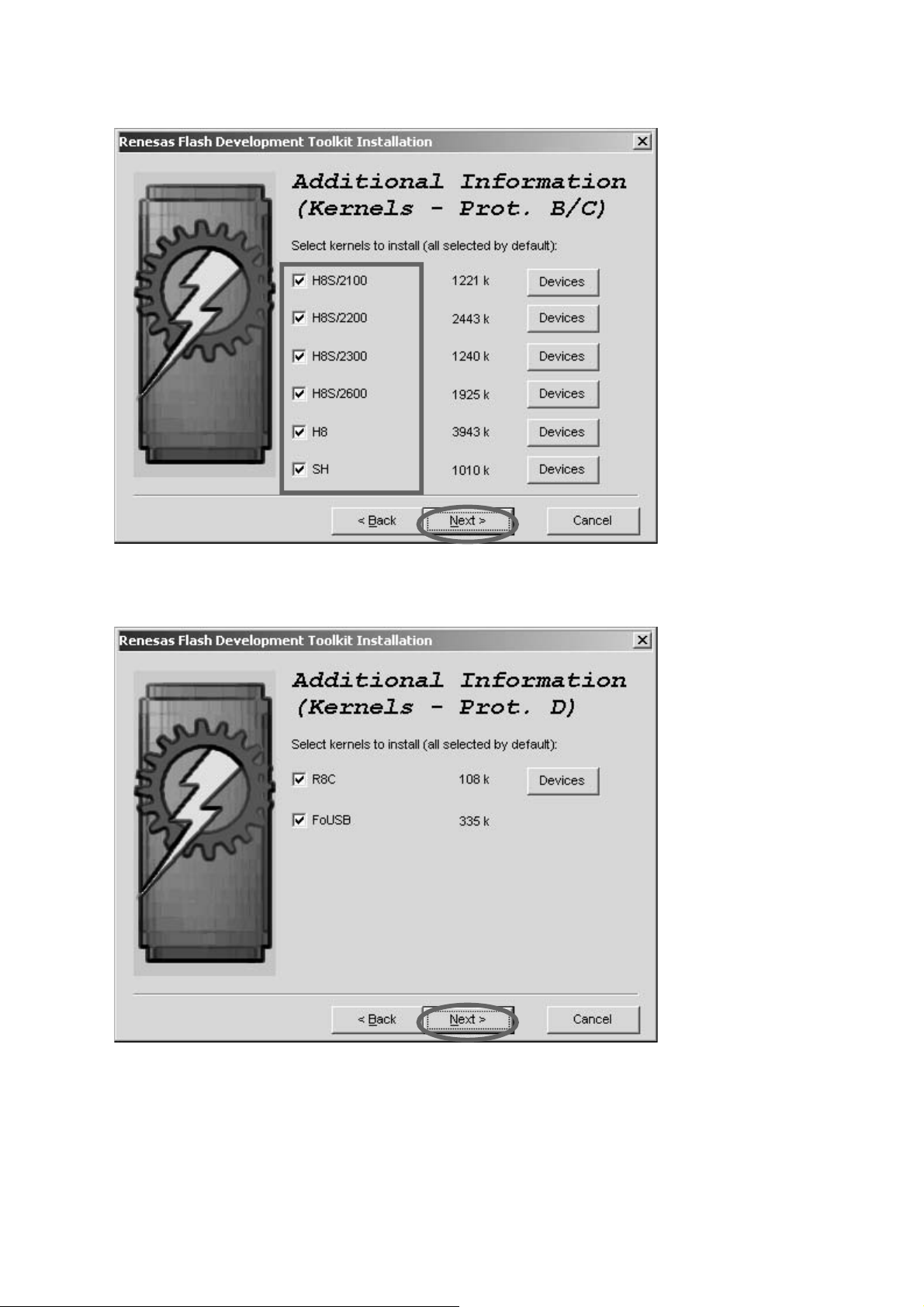
Check to the all check box. And click Next >.
全てのチェックボックスにチェックが入っていることを確認
し、
Next > をクリックします。
Click Next >.
をクリックします。
Next >
21
Page 24
Click Next >.
Next > をクリックします。
Click Next >.
Next > をクリックします。
22
Page 25
Click Next >.
Next > をクリックします。
Click Install.
Install をクリックします。
23
Page 26
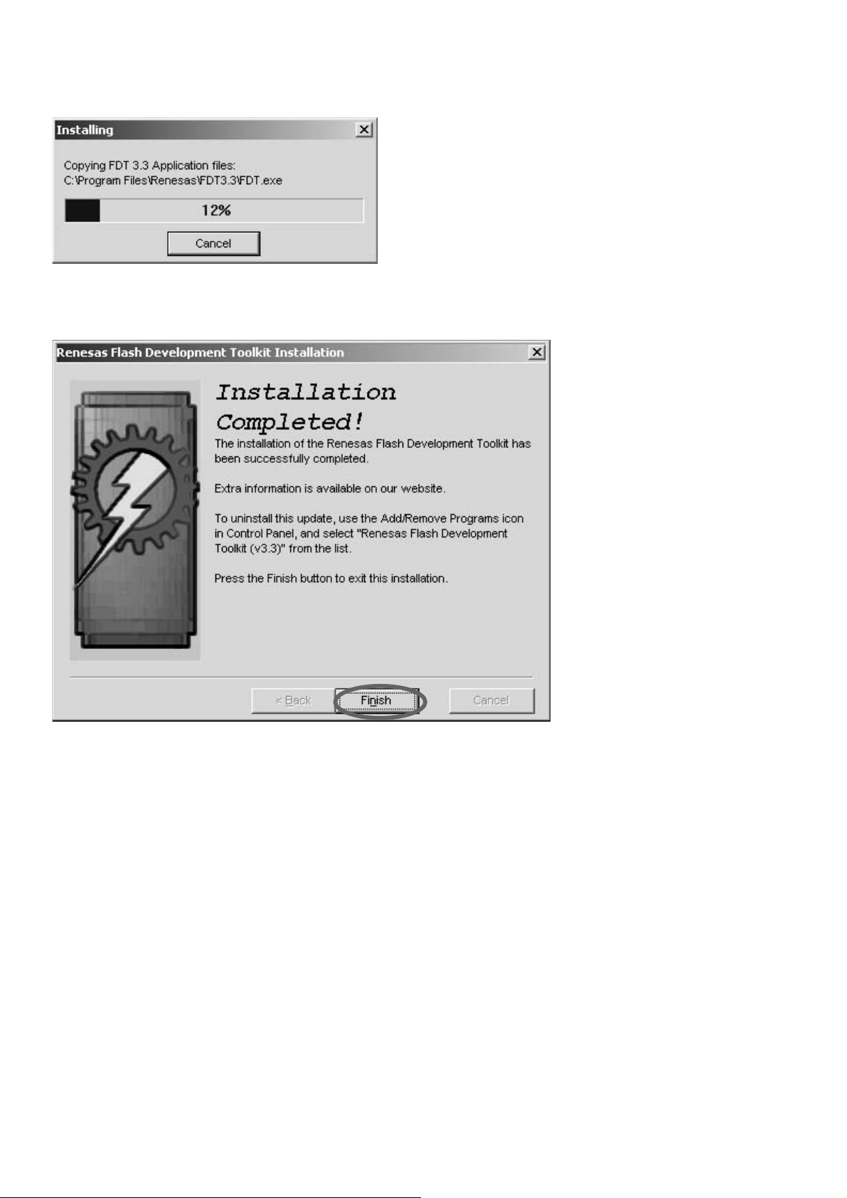
The status bar appears.
インストールを開始します。
Click Finish.
Finish をクリックしてインストールを完了します。
24
Page 27
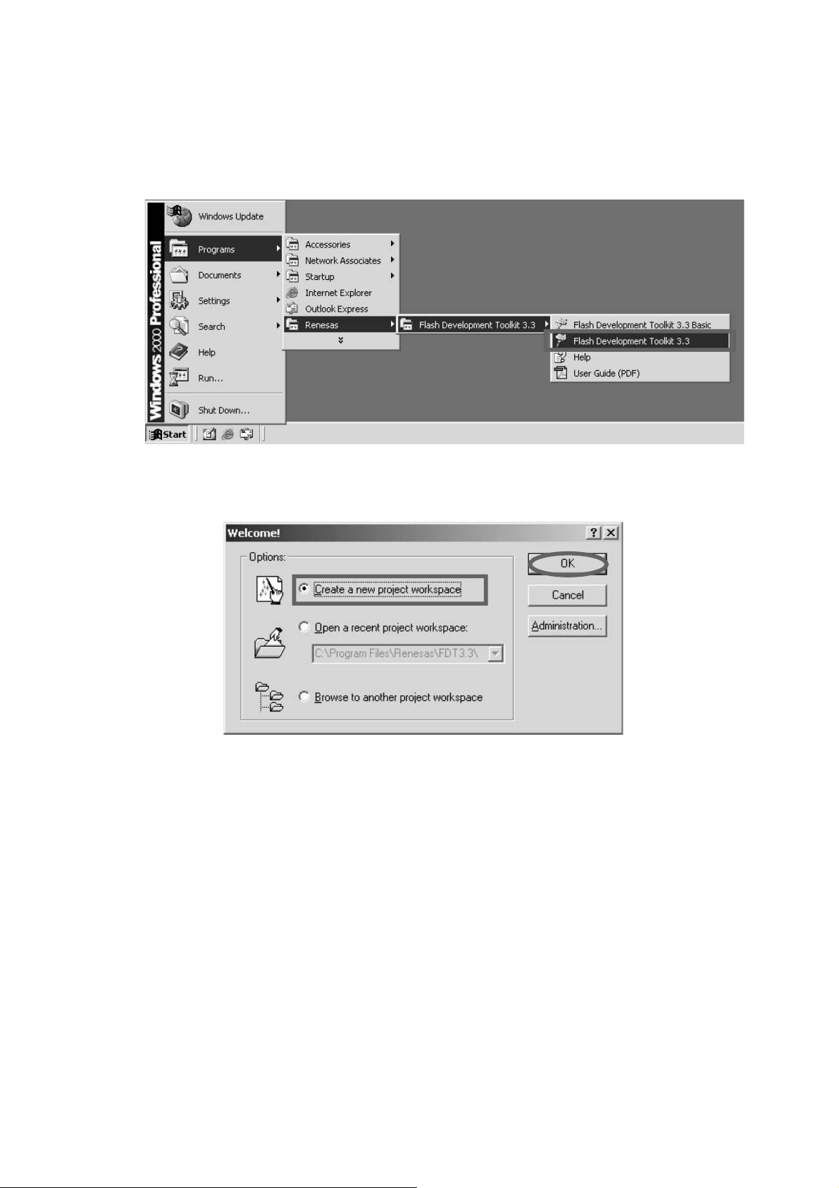
2. The writing software setup pro ce dure.
Launch up the writing software.
Click Start, Programs, Renesas, Flash Development
Toolkit 3.3 and Flash Development Toolkit 3.3.
(Although operation explanation by FDT3.3 is given
here, FDT3.0 is same operation too.)
2. 書き込みソフトウェアの設定
Start → Programs → Renesas → Flash Development
Toolkit 3.3
クします。
→ Flash Development Toolkit 3.3 をクリッ
( ここでは FDT3.3 での操作説明をしますが、
FDT3.0 も同じ操作になります。)
Check Create a new project workspace, and click OK.
Create a new project workspace にチェックを入れ、
OK をクリックします。
25
Page 28
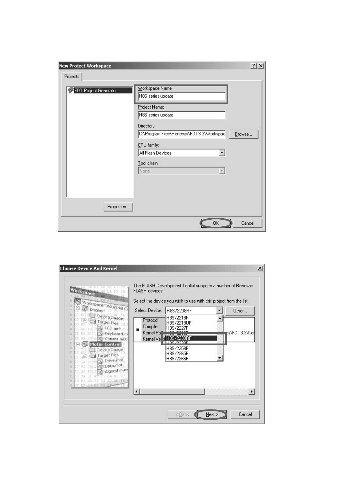
H8S series update is inputted into the Workspace
name. (It is si mul ta neous ly inputted into Project Name.)
Click OK.
Workspace Name に H8S series update と入力します。
( 同時に Project Name にも入力されます。)
をクリックします。
OK
Choose the H8S/2238RF in Se lect Device.
Click Next.
Select Device から H8S/2238RF を選びクリックします。
Next をクリックします。
26
Page 29
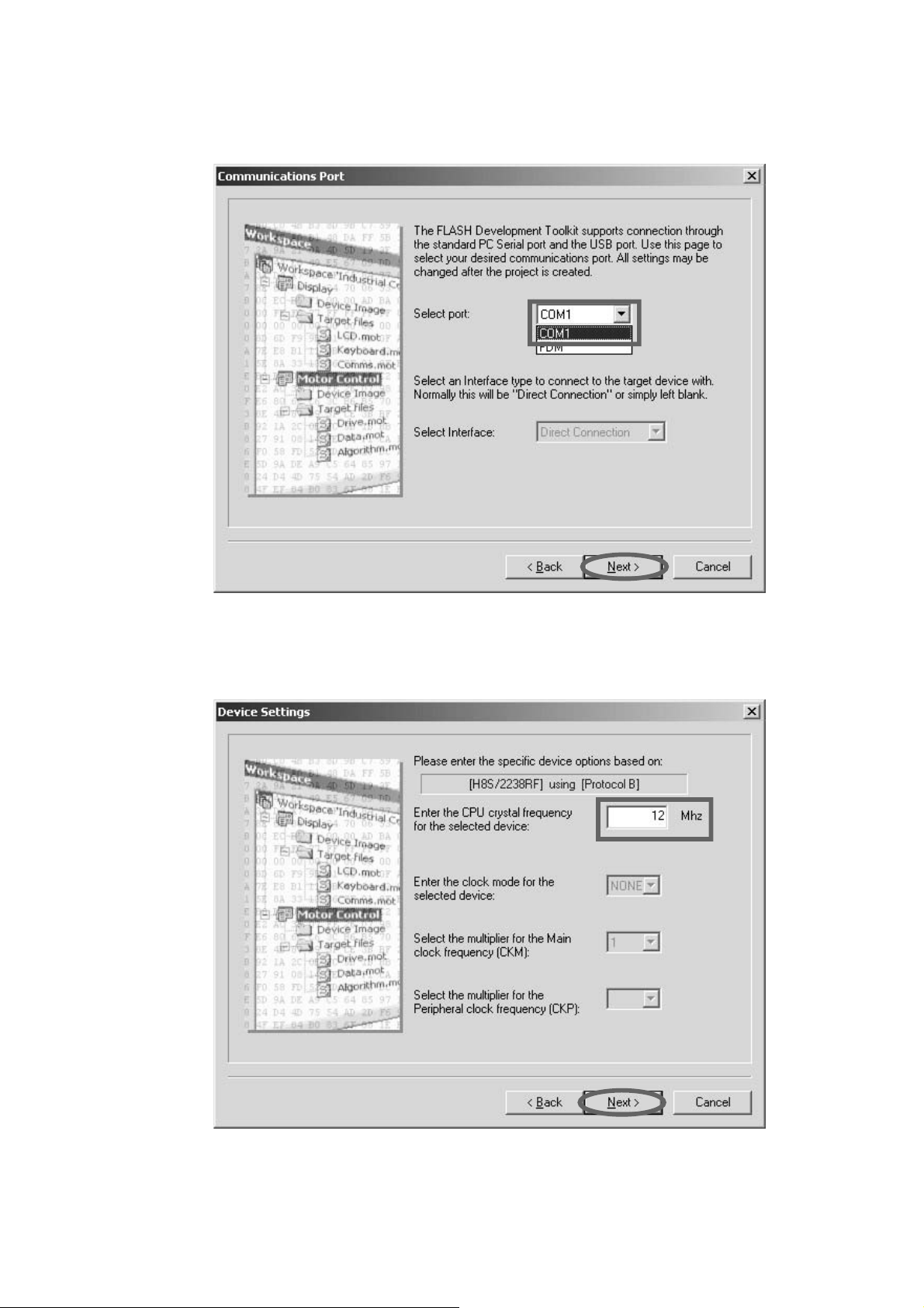
Choose the Serial port No. in the Se lect Port.
Click Next.
Select Port から接続する Serial Port 番号を選びクリック
します。
Next をクリックします。
12 is inputted into the Enter the CPU crystal frequency
for the selected device.
Click Next.
Enter the CPU crystal frequency for the selected
device:
に 12 と入力します。
Next をクリックします。
27
Page 30
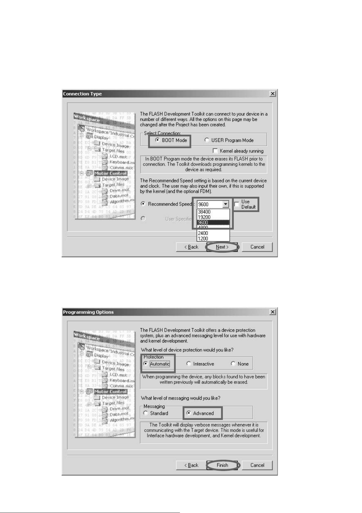
Check the BOOT Mode in Select Con nec tion.
Choose the 9600 in Select Baud rate.
Remark: Please remove check mark, if it is contained
in Use De fault.
Select Connection: から BOOT Mode にチェックを入れ
ます。
Select Baud rate: から 9600 を選びクリックします。
注意
) Use Default にチェックが入っていると Baud Rate
を変更できませんのでチェックを外してください。
Check the Automatic in Pro tec tion.
Check the Advanced in Mes sag ing.
Click Finish.
Protection から Automatic にチェックを入れます。
Messaging から Advanced にチェックを入れます。
Finish をクリックします。
以上で設定は完了です。
28
Page 31

3. Writing Procedure
When you carry out continuously from "2. The writing
software set up procedure", please move on to "Cable
connection" of next page.
Software is launched when the writ ing software is being
terminated.
Click Start, Programs, Renesas, Flash Development
Toolkit 3.3 and Flash Development Toolkit 3.3.
Check Browse to another project workspace, and
click OK.
3. 書き込み方法
インストールから引き続いて作業をしている場合は次頁の
「
PC と DVD Player の接続 」 に進んでください。
書き込みソフトウェアを終了させている場合は
Start →
Programs → Renesas → Flash Development Toolkit
→ Flash Development Toolkit 3.3 をクリックして起
3.3
動します。
Browse to another project workspace にチェックを入
れて
OK をクリックします。
Click the H8S series update.AWS, and click Open.
Remark: The file is stored in c:\Program Files\Renesas\
FDT3.3\Workspace\H8S series update.
H8S series update.AWS をクリックして、Open をク
リックします。
注意)
ファイルは c:
Workspace
ます。
\
rogram Files
P
\
S series update に格納されてい
H8
\
enesas
R
\
FD
T3.3
\
29
Page 32

Cable connection
PC (Windows 2000, XP )
with RS-232C port
PC と DVD Player の接続
RS232C Dsub-9 pin cable
(female to female/Straight cable)
Hole
ST81
Connect RS-232C on the rear pan el of the DVD Player
and Serial Port of windows PC with RS-232C cable.
Insert a thin rod to the hole near the RS-232C Port and
push the switch inside to turn on the switch.
Turn on by the POWER switch of DVD Player.
The DVD Player’s STANDBY (red) and DISPLAY OFF
(red) in di ca tors turn on lights simultaneously.
Windows PC の Serial Port と DVD Player の RS-232C
を RS-232C ケーブルで接続します。
Port
細い棒を使い
ある穴からスイッチ
ります。
DVD Player の RS-232C Port の右となりに
(ST81) を押して書き込みモードに入
DVD Player の Front Panel にある電源スイッチを押して電
源を入れます。
DVD Player の STANDBY( 赤 )、DISPLAY OFF( 赤 ) が点
灯します。
30
Page 33

Click Device in the menu bar and select Connect to
Device.
書き込みソフトウェアの Device から Connect to Device
を選びクリックします。
Error message will be displayed when an error occurs.
Check the connection cable and select Con nect to
Device again.
The following message is dis played that DVD Player
connects with PC.
接続に失敗すると下記のようなメッセージが出ます。ケー
ブル、接続を確認してもう一度
てください。
Connect to Device を行っ
PC と DVD Player の接続に成功すると下記のようなメッ
セージが出ます。
31
Page 34

Click File in the menu bar and se lect Open An
S-Record....
File から Open An S-Record... を選びクリックします。
xxxxx.mot is selected. And click Open.
update data の xxxxx.mot をクリックして Open をクリッ
クします。
32
Page 35

Click Device in the menu bar and select Download
Active File.
Device から Download Active File を選びクリックしま
す。
Software is written into the Panel microprocessor.
書き込みが開始され左下にステータスバーが出ます。
33
Page 36

The following message is dis played when the writing of
software was completed.
書き込みが完了すると下記のようにメッセージが表示され
ます。
Click Device in the menu bar and select Disconnect.
Device から Disconnect をクリックします。
The following message is dis played that DVD Player
disconnects with PC.
DVD Player との接続が切断されたメッセージが表示され
ます。
34
Page 37

Click File in the menu bar and se lect Exit.
RS232C Dsub-9 pin cable
(female to female/Straight cable)
Hole
ST81
PC (Windows 2000, XP )
with RS-232C port
File から Exit をクリックして書き込みソフトウェアを終了
します。
Turn off by the POWER switch in the front panel of DVD
Player.
After The DVD Player’s STANDBY (red) and DISPLAY
OFF (red) in di ca tors turn off lights, Insert a thin rod to
the hole near the RS-232C Port and push the switch
inside to turn off the switch.
Disconnect RS-232C cable of the DVD Player and Serial
Port of win dows PC.
DVD Player の Front Panel にある電源スイッチを押して電
源を切ります。
STANDBY, DISPLAY OFF のランプが消灯したら
RS-232C の右横の穴からスイッチを押し書き込みモード
を解除します。
RS-232C のケーブルを外します。
35
Page 38

7. SERVICE MODE
7. SERVICE MODE
Press the POWER ON/OFF button while pressing STOP and
FL OFF buttons in front panel of DVD Player.
The front display indicates "S-MODE_NO.".
Press the 1, 4, 3 and PLAY buttons of the remote controller
in order, while indicating "S-MODE_NO.".
The front display indicates "SERVICE_2".
SERVICE_2
Press NEXT on front panel.
MODE 1 Bx.xx (B/E microprocessor Version No.: 5 digits)
Press PLAY on front panel.
Press NEXT/PREV. on front panel.
MODE 2 Px.xx (Panel microprocessor Version No.: 5 digits)
Press PLAY on front panel.
Press NEXT/PREV. on front panel.
MODE 3 Axxxx (CODE for audio DSP Version No.: 5 digits)
Press PLAY on front panel.
Press NEXT/PREV. on front panel.
MODE 4 REGION x (Region No.)
Press PLAY on front panel.
Press NEXT/PREV. on front panel.
MODE 5 BIDxxxxxxxxx (DVD AUDIO ID No.: B/E microprocessor)
Press PLAY on front panel.
Press NEXT/PREV. on front panel.
MODE 6 PIDxxxxxxxxx (DVD AUDIO ID No.: Panel microprocessor)
Press NEXT/PREV. on front panel.
MODE 7 (DON’T USED)
Press NEXT/PREV. on front panel.
MODE 8 (DON’T USED)
Press NEXT/PREV. on front panel.
DVD Player のフロントパネルにある STOP と FL OFF ボタン
を押しながら
フロントディスプレイに
この表示が出ている間に
PLAY を押します。
フロントディスプレイに
POWER ON/OFF ボタンを押します。
S-MODE_NO. と表示されます。
(10 秒間 ) リモコンから 1、4、3、
SERVICE_2 と表示されます。
36
Page 39

8. WRITE-IN ID DATA FOR DVD AUDIO
PROCEDURE
A case writing is needs
Writing is needed when Q103 (PM01) was replaced.
8. DVD AUDIO 用 ID データの書き込み方法
書き込みが必要なとき
Q103(PM01) を交換したときに書き込みが必要になります。
Necessary Equipment
Windows PC (With Serial Port)
RS-232C Cable straight type (9 Pin female - 9 Pin female)
Writing software (CPPMset.exe)
ID data and ID number
Remark: Only one ID data and ID number are assigned to
the serial number of DVD Player., Beforehand,
please ask cus tom er center "ID data" and" ID
number" corresponding to the serial number of
DVD Play er.
Writing time
The writing of ID data for DVD AUDIO takes about 2
sec onds.
Writing procedure
1. Put the "CPPM" folder into anywhere on your PC’s hard
disc.
2. Move ID data suitable for the serial number ordered in
ad vance to the "DeviceKey" folder in a "CPPM" folder.
Remark: Please set only to one ID data put on a
"DeviceKey" folder. If two or more ID data is
placed, writ ing may not be made correctly.
3. Open the "CPPM.ini" in a "CPPM\marantz" folder by text
editors, such as Note pad.
必要機器
Windows PC (Serial Port 付き)
RC-232C ケーブル (9pin メス− 9Pin メス ストレートタイプ )
書き込みソフト (CPPMset.exe)
データと ID ナンバー
ID
: ID データと ID ナンバーは DVD Player のシリアルナン
注意
バーに対して
う際は
データと ID ナンバーを事前にカスタマーセンターより取
り寄せてください。
書き込み時間
この
DVD AUDIO 用 ID データの書き込み時にかかる時間はお
よそ
2 秒です。
書き込み手順
1 つ割り当てられています。書き込みを行
DVD Player のシリアルナンバーに対応した ID
1. Windows PC の任意のフォルダに CPPM フォルダをコ
ピーします。
2. 事前に取り寄せたシリアルナンバーに合った ID データを
CPPM フォルダ内の DeviceKey フォルダに移動します。
注意: DeviceKey フォルダに置く ID データは 1 つだけ
にしてください。複数の
書き込みが出来ない場合があります。
ID データを置くと正しく
3. CPPM\marantz フォルダ内にある CPPM.ini を Note pad
などのテキストエディタで開きます。
37
Page 40

4. Type in the serial number of DVD Player to the first line.
And type in ID number to the second line.
4. 一行目に DVD Player のシリアルナンバーを入力します。
二行目に
ID ナンバーを入力します。
Input the 14 digits serial number.
Input the 9 digits ID number.
14桁のシリアルナンバーを入力
9桁のIDナンバーを入力
5. Click the "Save Ctrl+S" in the File.
5. File から Save Ctrl+S をクリックして保存します。
38
Page 41

6. Click the "Exit" in the File.
6. File から Exit をクリックして閉じます。
7. Connect RC-232C on the rear panel of DVD Player and
Serial Port of windows PC with RS-232C cable.
8. Turn on the power of DVD Player into the writing mode.
8.1 Press the POWER ON/OFF button while pressing
STOP and FL OFF buttons in front panel of DVD
Play er.
8.2 The front display indicates "S-MODE_NO.".
8.3 Press the 1, 2, 1 and PLAY buttons of the remote
con trol ler in order, while indicating "S-MODE_NO.".
8.4 The front display indicates "AUDIO_ID".
9. Double click the "CPPMset.exe" in the CPPM\marantz
fold er.
7. Windows PC の Serial Port と DVD Player のリアパネル
にある
RS-232C コネクタを RS-232C ケーブルで接続し
ます。
8. DVD Player を CPPM 書き込みモードにします。
8.1 DVD Player のフロントパネルにある STOP と FL
ボタンを押しながら POWER ON/OFF を押し
OFF
ます。
8.2 フロントディスプレイに S-MODE_NO. と表示され
ます。
8.3 この表示が出ている間に (10 秒間 ) リモコンから 1、2、
1、PLAY を押します。
8.4 フロントディスプレイに AUDIO_ID と表示されます。
9. CPPM\marantz フォルダ内の CPPMset.exe をダブルク
リックします。
39
Page 42

10. The picture shown below is displayed. Check the serial
number (S/N), ID number (ID), and ID data are right.
10. ID 書き込みソフトが立ち上がります。シリアルナンバー
(S/N)、ID ナンバー(ID)と ID データが正しいか確認し
てください。
11. Check the Serial Port number. When serial port
numbers dif fer, Press the C key of a keyboard, input the
right serial port number, and press the Enter key and
changed.
11. Serial Port の確認をします。接続した Serial Port
Num ber
と違う場合はキーボードの C を押し、接続した
Se ri al Port Number を入力してキーボードの Enter を押
して変更します。
40
Page 43

12. Press the space key of a keyboard and write ID data
into the DVD Player.
13. Display "Under transmission...". And terminates the
soft ware automatically, when writing was completed.
The writ ing of ID data for DVD AUDIO takes about 2
seconds.
12. キーボードのスペースキーを押して、ID データを DVD
書き込みます。
Player
13. Under transmission... と表示され、書き込みが完了する
とソフトウェアは自動的に閉じます。転送にかかる時間は
およそ
2 秒です。
14. Please check written-in ID data by MODE5 and MODE6
of SERVICE MODE.
14. 書き込まれた ID データの確認は SERVICE MODE の手順
に従い
MODE5、MODE6 にて確認してください。
41
Page 44

9. TROUBLESHOOTING
1. Power Supply PWB (P801)
1.1 The power cannot be turned on.
Is the E+6V voltage line (J808) normal?
OK
Is the control signal of J305 (10pin)
normal? STB_CTRL=H
OK
Is the each voltage line normal?
+12V, +8V, +5V_D2, D+4V, -27V,
DC+3.5V and HEATER
NG
NG
NG
• Check the fuse (F801) has not blown
out.
• Check the voltage inputted/outputted to
each pin of Q801, Q802 and Q803.
Note: When checking the primary circuit,
the GND of a measuring instrument
should be switched floating.
Refer to “3.1 Check the panel
microprocessor”.
Check the voltage inputted/outputted to
each pin of the connected components.
42
Page 45

2. DISPLAY CONTROL PWB (PF01) / PHONE PWB (PH01)
2.1 FL is not outputted.
Is the connector (JF02) voltage line
normal?
+5V_D1, -27V, DC+3.5V and HEATER
OK
Is the 61pin of the QF71 line H?
OK
NG
NG
Check the soldering of these componentson
the POWER SUPPLY PWB (P801) and
DISPLAY CONTROL PWB (PF01).
Check the 8pin of QF80 Signal.
Reset = H
NG OK
Check the soldering of RF72
and CF74.
Check the Signal of QF80 (9pin).
Reset = H
NG
OK
Replace QF80.
Check the soldering of RF11, RF80,
CF11, CF81, JF01 (12pin) and
QU01 (71pin).
Are the 62,63 and 64 pin of QF71 signal
normal? (H L)
OK
Are the 1 to 40pin and 42 to 54pin of
QF71 signal normal? (H L)
OK
Replace VF01.
NG
NG
Check the 2,5 and 12 pin of QF80 signal.
(H L)
NG
OK
Replace QF80 or / and QF71.
Check the soldering of RF08, RF09,
RF10, JF01 (8,10,11pin) and QU01
(9,70,73pin).
Replace QF71.
43
Page 46

2.2 No sound is output from Phones. (The headphones are connected to PHONES jack.)
Are the connector (J950, J951) voltage
line normal? 8pin and 10pin,+8VA,–8VA
OK
Is the 1pin of connector (J950, J951)
voltage line normal?
HP connection: L / HP un-connecting: H
(3.3V)
OK
Is the 6pin of Q950 MCLK signal normal?
OK
Is the waveform of Q950 (3 to 5pin)
normal?
OK
Is the waveform of Q950 (14,15,19pin)
normal?
NG
NG
NG
NG
NG
Check the +8VA and –8VA voltage line of
PM01 PWB, PA01 PWB and P801 PWB.
Replace J952.
Check the MCLK signal of PM01 PWB.
Check the Audio data output line of
PM01 PWB.
Replace Q950
OK
Is the 2pin of connector (J950, J951)
voltage line normal?
PLAY: L (–8V), STOP: H (3V)
OK
Are the MUTE signals normal?
NG
NG
Check the HP-MUTE output signal of
PA01 PWB.
Replace defect component.
44
Page 47

3. Main PWB (PM01)
3.1 Check the panel microprocessor
Are the E+6V and E+3.3V of QU91
voltage lines normal?
OK
Is the reset signal of QU01 (59pin) normal?
OK
Is the master clock waveform normal?
12.000MHz
OK
Is not QU01 write-in mode?
67pin=H, 66pin=L
OK
Is each output voltage normal?
(After the 15pin of QU01 changed to H)
OK
NG
NG
NG
NG
NG
• E+6V=0V: Check the E+6V voltage line
on POWER SUPPLAY PWB (P801).
• E+3.3V=0V: Check the soldering of
QU01, or replace QU91.
Check the soldering and the input/output
voltage of QU03.
Check the soldering XU01 and QU01
(63pin and 65pin).
Check the soldering of ST81, CT86 and
QU04.
OK
Replace QU04.
Refer to “1. POWER SUPPLAY PWB (P801)”.
Is communication to QT01 and QU01
(78pin and 79pin) normal?
OK
Is communication to Q301 and QU01
(75pin and 79pin) normal?
Is 88pin of QU01 H?
OK
Is communication to Q102 normal?
Is 28pin of QU01 H?
Is communication of 38pin, 83pin, 84pin
and 85pin on QU01 normal?
OK
Finish
NG
NG
NG
• Check the soldering of QT01,
circumference components and power
supply line.
• Check the soldering QT05, QW81,
QW01, QW02 and QW03.
• Check the output voltage of QT05 and
QW81.
• Check the soldering of Q301, Q302,
RU72, RU73 and RU74.
• Check the power supply line of Q301.
• Check the frequency of 126pin on Q301.
(12.288MHz)
Refer to “3.2 Check the B/E microprocessor”.
45
Page 48

3.2 Check the B/E microprocessor
Are the +3.3V_D1 and +2.5V_D2 of Q102
voltage lines normal?
OK
Is the clock waveform of 18pin on Q102
normal? (27MHz. 2Vp-p)
OK
Is the 15pin of Q102 H?
OK
NG
NG
NG
Check the soldering of Q117 and Q116,
and the input/output voltage.
NG
OK
Input voltage is OK: Check
the soldering of circumference
components of Q102.
Soldering is OK: Replace
Q117 or Q116.
Refer to “1. POWER SUPPLY PWB (P801)”.
Check the waveform of 4pin on Q105.
(27MHz 2Vp-p)
NG
OK
Check the soldering of R168
and R153.
Check the soldering of X101, circumference
components and Q105.
Check the soldering of QU01 (28pin),
R156 and C161.
Are the +3.3V_D1 and +1.8V_D1 of Q101
voltage lines normal?
OK
Is the clock waveform of 18pin on Q106
normal? (27MHz. 2Vp-p)
OK
Refer to B/E 2.
NG
NG
Check the soldering of Q118, and
the input/output voltage.
OK
Input voltage is OK: Check the soldering
of Q101.
Soldering is OK: Replace Q118.
Check the waveform of 3pin on Q105.
(27MHz 2Vp-p)
NG
OK
Check the soldering of R170
and R101.
Check the soldering of X101,
circumference components and Q105.
46
Page 49

B/E 2
Is the clock waveform of 172pin on Q101
normal? (24.576MHz. 2Vp-p)
OK
Is the 193pin of Q101 H?
OK
Is communication of the data bus on Q102
and Q103 normal?
OK
NG
NG
NG
Check the waveform of 9pin on Q105.
(24.576MHz 2Vp-p)
NG OK
Check the waveform of 6pin
on Q111. (24.576MHz)
OK
Check the soldering of R175
and R133.
Check the soldering of X101,
circumference components and Q105.
Check the soldering of Q102 (114pin),
R124, R143, C135 and Q101 (193pin).
Check the soldering of data bus lines.
(MCD0-MCD14 and MCA11-MCA30)
Finish
47
Page 50

3.3 Check the F/E microprocessor.
Are the +3.3V_D2, +1.8V_D2, +3.3V_A2
and +1.8V_A2, of Q502 voltage lines
normal?
OK
Is the clock waveform of 33pin on Q502
normal? (33.87MHz. 2Vp-p)
OK
NG
NG
• Check the soldering of Q114, Q115, and
the input/output voltage.
• Check the soldering of L404, L407 and
circumference components.
NG OK
Check the soldering of
the Q502 and circumference
components.
OK
Replace Q114 or Q115.
Refer to “1. POWER SUPPLY PWB (P801)”.
Check the waveform of 15pin on Q105.
(33.87MHz 2Vp-p)
NG OK
Check the waveform of 2pin
on Q111. (33.87MHz)
OK
Is the 51pin of Q502 H?
Finish
OK
NG
Check the waveform of 2pin
on Q405. (33.87MHz)
OK
Check the soldering of R491
and R574.
Check the soldering of X101,
circumference components and Q105.
Check the soldering of Q102 (108pin),
R129, R570, R648 and C638.
48
Page 51

3.4 Check the DIGITAL VEDEO OUTPUT.
Are digital output signals of Q101 normal?
PXD(0-7), VCLK(27MHz)
OK
Is the reset signal normal?
Q109 (9pin) = H
OK
NG
NG
Check the soldering of Q101 (183-192pin),
R201, R202 and R125.
OK
Refer to “3.1 Check the panel
microprocessor”.
Check the 11pin on Q109.
(Change to H from L, after turn on the unit.)
Check 8pin on Q109 H?
NG OK
Check the soldering of R189,
R190, R191 and Q108.
OK
Replace Q108.
Check the soldering R192 and Q109.
OK
Is communication to QK01 of digital
signals normal?
Check that 13pin, 16pin, 3-10pin and 137pin.
OK
Are the VD+3.3V and VD+1.8V voltage
lines of QK01 normal?
OK
NG
NG
Replace Q109.
Check the soldering of QK10, QK11 and
circumference components.
OK
Check theVD+3.3V line and soldering of
LK34.
OK
Replace QK10 or QK11.
Check the soldering of QK91, QK92 and
circumference components.
Check the soldering of LD01and LK02.
OK
Check the E+4V voltage line.
OK
Replace QK91 or QK92.
Refer to Video 2
49
Page 52

Video 2
Is the IIC waveform of 162pin and 165pin
on QK01 normal?
OK
Is communication of the data bus and
address line between QK03 and QK01
normal?
OK
NG
NG
Check the IIC waveform of 1pin on QK07
and QK08.
NG OK
Check the soldering of RK28,
RK29, QK07 and QK08.
OK
Replace QK07 or QK08.
Check the soldering of Q102 (57pin and
58pin), R160 and R161.
OK
Refer to Refer to “3.1 Check the panel
microprocessor”.
Check the VD+3.3V voltage line.
NG OK
Check the soldering of QK03,
RK14-26, RK31-33 and RK94.
OK
Are digital outputs of QK01 normal?
PY(0-9), SD(0-9), SDVSYNC,
SDHSYNC, SDCLK (27MHz) and
SDCLK2 (27MHz)
OK
Finish
Refer to “Check the Video encoder” or
“Check the HDMI PWB (PD01)”.
NG
Replace QK01 or QK03.
Check the soldering of LK03, CK30 and
CK31.
Check the soldering of QK01 (from 61 to
99 pin).
OK
Replace QK01 or QK03.
50
Page 53

3.5 Check the Video encoder. (Component, CVBS, Y/C)
Are the VD+3.3V and +2.5AD voltage lines
of QM01 normal?
OK
Is the reset signal of QM01 (33pin)
normal?
VRST_5=H
OK
Are the digital data of QM01 normal?
2-9pin, 12-18pin, 26-30pin, 51-55pin and
58-62pin
NG
NG
NG
Check the soldering of QM01, LM01, LM02,
LM03, QK91 and QM91.
OK
Check the input voltage of QK91 and QM91.
NG
OK
Replace QK91 or QM92.
Refer to “POWER SUPPLY PWB (P801)”.
Check the soldering of QK10 (18pin),
RM12 and CM09.
OK
Refer to “3.4 Check the DIGITAL VIDEO
OUTPUT”.
Check the soldering of RM01-05, RM26-29
and QM01.
OK
OK
Is the master clock waveform of 32pin on
QM01 normal? 27MHz 2Vp-p
OK
Is the IIC waveform of 21pin and 22pin on
QM01 normal?
OK
Are the video signals outputted to each pin
of JM01?
1pin=video, 3pin=S-C, 5pin=S-Y,
7pin=component-Y, 9pin=Cb, 11pin=Cr
OK
NG
NG
NG
Refer to “3.4 Check the DIGITAL VIDEO
OUTPUT”.
Check the soldering of RM11 and QM01.
OK
Refer to “3.4 Check the DIGITAL VIDEO
OUTPUT”.
Check the soldering of RM08, RM09 and
QM01.
OK
Check the soldering of QK07 and QK08.
OK
Refer to “3.4 Check the DIGITAL VIDEO
OUTPUT”.
Check the soldering of QM02-QM07 and
circumference resistors.
OK
Check the output signals of QM01
(37-39 pin and 42-44pin).
OK
Finish
Replace QM02-QM07.
51
Page 54

3.6 Check the Video encoder. (RGB)
Are the VD+3.3V and +2.5AD voltage
lines of QN01 normal?
Is the reset signal of QN01 (33pin)
normal?
VRST_5=H
OK
Are the digital data of QN01 normal?
51-55pin and 58-62pin
OK
NG
NG
NG
Check the soldering of QN01, LN01, LN02,
LN03, QK91 and QM91.
OK OK
Check the input voltage of QK91 and QM91.
NG
OK
Replace QK91 or QM92.
Refer to “POWER SUPPLY PWB (P801)”.
Check the soldering of QK10 (18pin),
RN06 and CN09.
OK
Refer to “3.4 Check the DIGITAL VIDEO
OUTPUT”.
Check the soldering of RM23-26 and QN01.
OK
Is the master clock waveform of 32pin on
QN01 normal?
27MHz 2Vp-p
OK
Is the IIC waveform of 21pin and 22pin on
QN01 normal?
OK
Are the video signals outputted to each
pin of JN01?
4pin=G, 6pin=B, 8pin=R
NG
NG
NG
Refer to “3.4 Check the DIGITAL VIDEO
OUTPUT”.
Check the soldering of RN05 and QN01.
OK
Refer to “3.4 Check the DIGITAL VIDEO
OUTPUT”.
Check the soldering of RN02, RN03 and
QN01.
OK
Check the soldering of QK07 and QK08.
OK
Refer to “3.4 Check the DIGITAL VIDEO
OUTPUT”.
Check the soldering of QN02-QN04 and
circumference resistors.
OK
Finish
OK
Check the output signals of QN01
(37-39pin).
OK
Replace QN02-QN04.
52
Page 55

3.7 Check the Playback disc.
3.7.1 Loader is not rotate.
Is the laser beam light up?
Is the current of laser beam normal?
OK
Is Spindle drive signal normal? DM0=H
OK
Finish
3.7.2 CD playback
Is the RF signal normal?
RFAC test pint=approximately 1Vp-p
OK
Is communication of Q502 and Q503
normal?
OK
Finish
NG
NG
NG
NG
• Check the unsoldering of protection
solder pad on the pickup.
• Check the soldering of Q510 and
circumference components of Q511.
• Check the connection of F506 and
pickup connector.
• Check the soldering of Q501.
• Check the soldering of Q508.
• Check the soldering Q502 (111-113pin).
• Check the soldering R615, R699 and
R666-669.
• Check the soldering Q505.
• Check the soldering of Q501 and
circumference components.
• Check the soldering of Q502 (from 65 to
110 pin).
• Check the soldering Q502 and Q503.
• Check the soldering of data bus lines.
BD(0-15), BA(0-9)
• Check the soldering of XLCAS, XUCAS,
XMOE, XRAS and XMWR.
3.7.3 DVD playback
Is communication of VSTEM between
Q502 and Q404 normal? VDT(0-7)_COR,
XHAC_COR, VEFG_COR, XSHD_COR
and DCK_COR
OK
Is the Request signal normal?
HDRQ_COR=L, Q502 (45pin),
Q404 (21pin)
OK
Finish
NG
NG
• Check the soldering of Q502 (from 36 to
49pin).
• Check the soldering of R621-R633.
• Check the soldering of R401-R412.
Check the soldering of Q404.
53
Page 56

3.7.4 Super Audio CD playback
Is communication of VSTEM between
Q404 and Q401 normal?
SD(0-7), SDCK, XSRQ, SDEF and
XSHD2.
OK
Is the RF signal normal?
WM test pint (Q403: 1pin)=approximately
1Vp-p
OK
Is communication of the data bus line
between Q401 and Q402 normal?
OK
Finish
3.8 No sound or noisy
3.8.1 CD playback
Are the CD digital audio data output
signals of Q101 normal? CDLRCK,
CDBCLK, CDDIN and DOTX
OK
NG
NG
NG
NG
Check the soldering of Q404, and
R437-R449.
Check the soldering of Q403 and
circumference components.
Check the soldering of Q401, R141-R162
and Q402.
• Check the soldering of Q502 (from 58 to
62).
• Check the soldering of R641-R644.
Are digital audio data output signals of
Q101 normal?
DATA1, LRCK, BCK and DOUT0
OK
Are the output signals of PCM/DSD
selector normal? MCLK, DABCK, DAD0
and DSDR
OK
Refer to “6. AUDIO PWB (PA01)”.
NG
NG
• Check the soldering of Q101 (from 159
to 170 pin).
• Check the soldering of R134-R142.
• Check the soldering of Q204-Q207.
• Check the soldering of Q105 and Q111.
54
Page 57

3.8.2 DVD-Video/Audio playback
Are the DVD digital data output signalsof
Q101 normal?
0DATA(1-3), 0LRCK and 0BCK
OK
Are bass management output signals of
Q301 normal?
IBCK, ILRCK, IDT0, IDT1 and IDT2
OK
Are the output signals of PCM/DSD
selector normal?
MCLK, DABCK, DAD0, DSDR, DAD1,
DSDSW, DAD2 and DSDRS
OK
NG
NG
NG
• Check the soldering of Q101 (from 159
to 171 pin).
• Check the soldering of Q304.
• Check the +3.3V_D1 and +2.5VD1
voltage lines.
• Check the clock frequency on Q301.
12.288MHz
• Check the soldering of Q301 and Q302.
• Check the control signals of Q301.
DSPREQ1, FCS, DSPDIN,
DSPDCLOK, DSPREQ2, RSTDSP, SCS
and HINBSY
• Check the control signals (SPI) of Q304.
CDIN, CS3, CRST, CCLK and CDOUT
• Check the soldering of Q303 and Q305.
• Check the soldering of Q204-Q207.
• Check the soldering of Q203.
• Check the soldering of J271.
Refer to “6. AUDIO PWB (PA01)”.
3.8.3 Super Audio CD playback
Are the DSD data output signals of Q401
normal?
DSARS, DSALS, DSASW, DSAC, DSAR,
DSAL and BCKA0
OK
Are the output signals of PCM/DSD
selector normal?
MCLK, DABCK, DAD0, DSDR, DAD1,
DSDSW, DAD2 and DSDRS
OK
Refer to “6. AUDIO PWB (PA01)”.
NG
NG
• Check the soldering of Q401 (from 60
to76 pin).
• Check the soldering of R450-R456.
• Check the soldering of Q204-Q207.
• Check the soldering of Q203.
• Check the soldering of J271.
55
Page 58

4. HDMI PWB (PD01)
QW0
Q
4.1 Check the Scaler.
Are the SC+3.3V_1, SC+2.5V_1 and
SC+1.2V_1 voltage lines of QW01
normal?
OK
Is the reset signal of QW01 H?
RW12 VRST_3=H
OK
NG
NG
Check the soldering of LW01-LW03,
QW01 and QW81-QW83.
OK
Check the input voltage of QW81-QW83.
OK
Check the VD_PSW level. VD_PSW=L
OKNG
Replace QW81, QW82 or
QW83.
Check the soldering of JQ02, JK02 (8pin)
and QU01 (1pin).
Check the soldering of QW01, RW12.
OK
Check the soldering of JW02, JK02 (2pin)
and QU01 (24pin).
Are the digital data input signals normal?
PY_2䇼0-9䇽, SDCLK_2, SDHSYNC_2,
SDVSYNC_2, DE.
OK
Is the voltage lines of
QW05 normal?
19, 20pin 䋨SC+2.5V_1)
18pin (SC+3.3V_1)
NG
Check the soldering
of QW05, CW48-䌃
䌗50.
OK
Is the signal of QW05 H?
10pin (CONFIGDONE)=H
NG
#HECKTHESOLDERING
OF272䌗
/+
Check the soldering
of RW18-R䌗21 and
RW23.
NG
Check the soldering of JW01, JK01,
RW01-RW06, RW09, RW17, RW38 and
1.
OK
Check the soldering of QK05-QK06,
QK13 and circumference components of
K14.
OK
Check the input signals of
QK04-QK06.
NG
OK
Check the voltage
line QK04-QK06.
OK
NG
Replace
QK04-QK06.
Refer to “3.4 check the
DIGITAL VIDEO OUTPUT”
NG
Refer to Scaler 2
Replace QW05.
56
Page 59

Scaler 2
Is the PLLCLK of RW10 normal?
OK
Is the 30MHz CLK of XW0(2pin) and
XW0(3pin) normal?
OK
OK
NG
Check the soldering of
Is the waveform
of RW11
normal?
XW02 and
circumference
components.
Is the waveform of SD_RAM (RW59-61)
normal?
OK
Is the waveform of RW57-RW58 (each
pin) normal?
OK
Is the waveform of RW41-56 (each pin)
normal?
NG
NG
Check the soldering of RW10.
OK
Check the input voltage of QW04 and
LW05
OK
Check the input CLK of QW04(1pin).
NG
Check the soldering of RW26 and
circumference components of QW04.
Refer to Scaler 3
57
Page 60

Scaler 3
Is the IIC waveform of RW13 and RW14
(SDA1, SCL1) normal?
OK
Are digital output signals of QW01
normal?
HDB(0-9), HDG(0-9), HDR(0-9),
HDVSYNC, HDHSYNC, HDVCLK and
HDDE
OK
Finish
NG
NG
Check the soldering of RW13,
circumference components of RW14,
JW01 and JK01 (4,5pin).
OK
Check the waveform of QW02 (1pin) and
QW03 (1pin).
OKNG
Replace QW02 or QW03.
Check the soldering of QU01 (78, 79pin).
Replace HDMI PWB (PD01).
Notice
OUTPUT Format Frequency of HDVCLK Signal
720P 74.5MHz
1080i 74.5MHz
480P/480i 27MHz
576P/576i 27MHz
1080P 148.5MHz
58
Page 61

4.2 Check the HDMI driver.
Are the HDP+1.8V and HDP+3.3V
voltage lines of QT01 normal?
OK
Are input digital signals normal?
HDB(0-9), HDG(0-9), HDR(0-9), HDDE,
HDHSYNC, HDVSYNC and HDVCLK
OK
Is the reset signal (VRST_4) of QT01 H?
OK
NG
NG
NG
Check the soldering of QT01, QT07,
QT08 and LT01-LT04.
OK
Check the input voltage of QT07 and
QT08.
OKNG
Replace QT05 or QW81.
Check the soldering of JW02 and JK02.
OK
Refer to “1. POWER SUPPLY PWB (P801)”.
Check the soldering of QT01, RT01-RT03
and RT14-RT19.
Check the soldering RT27-RT29, QT02
and QT03 (25pin).
Is the IIC waveform of QT01 normal?
SDA1 and SCL1
OK
Is the picture of the television inputted by
HDMI normal?
OK
Finish
(Of course, there needs to be no problem
in video and audio output signal. And the
audio also checks HD_SPDIF.)
NG
NG
Check the soldering of QT01, RT30 and
RT31.
Check the soldering of JT01, LT06-LT09
and RT17-RT24.
OK
Check the soldering of QT04, QT05, LT05
and circumference components.
OK
Replace QT01.
59
Page 62

5. Check the analog video output signal : VIDEO PWB (PV01).
5.1 Picture is not outputted normally. (Com pos ite, Y/C)
Is the E+6V voltage line of JV05 normal?
OK
Is the +5VV voltage line of QV01 normal?
OK
Are the video signals inputted to each pin
of QV01?
4pin=video, 6pin=S-Y, 2pin=S-C
OK
Are the analog video signals outputted to
each pin of QV01?
13pin=video, 10pin=S-Y, 15pin=S-C
NG
NG
NG
NG
Refer to “1. POWER SUPPLY PWB (P801)”.
Check the output voltage of QV91.
+5VV
OK
Check the QV91 (1pin) level.
1pin=H
NG OK
Refer to “3.1 Check the panel
microprocessor”.
Replace QV91.
Refer to “3.4 Check the DIGITAL VEDEO
OUTPUT”.
Replace QV01.
60
Page 63

5.2 Picture is not outputted normally. (Com po nent)
Is the E+6V voltage line of JV05 normal?
OK
Is the +5VV voltage line of QY07 normal?
OK
Are the video signals inputted to QY01 (Y),
QY03 (Cb) and QY05 (Cr)?
OK
Are the video signals inputted to each pin
of QY07?
1pin=Y, 3pin=Cb, 5pin=Cr
NG
NG
NG
NG
Refer to “POWER SUPPLY PWB (P801)”.
Check the output voltage of QV91.
+5V
OK
Check the QV91 (1pin) level.
1pin=H
NG OK
Refer to “3.1 Check the panel
microprocessor”.
Replace QV91.
Refer to “3.4 DIGITAL VEDEO OUTPUT”.
Check the soldering of video filter block.
Y=QY01-QY02, Cb=QY03-QY04,
Cr=QY05-QY06
OK
Are the video signals outputted to each pin
of QY07?
9pin=Y, 11pin=Cb, 13pin=Cr
NG
Replace QY07.
61
Page 64

5.3 Picture is not outputted normally. (SCART)
Are the E+6V and SW+12 voltage lines of
JV05 normal?
OK
Is the +5VV line of QE01 normal?
OK
Are the video signals inputted to each pin
of QE01 and QE02?
QE01: 8pin=Y, 9pin=V, 11pin=C,
14pin=R,QE02: 10pin=B, 12pin=G
OK
NG
NG
NG
Refer to “1. POWER SUPPLY PWB (P801)”.
Check the output voltage of QV91.
+5V
OK
Check the QV91 (1pin) level.
1pin=H
NG OK
Refer to “3.1 Check the panel
microprocessor”.
Replace QV91.
Refer to “3.4 Check the DIGITAL VEDEO
OUTPUT”.
Are the video signals inputted to each pin
of QE02? 4pin=V/Y, 14pin=C/R
OK
Are the video signals outputted to each pin
of QE02?
16pin=C/R, 18pin=R, 20pin=B, 23pin=V/Y
NG
NG
Check the signal level of QE01 (12pin).
RGB/VIDEO output=H, S-VIDEO
output=L
NG
Refer to “3.2 Check the B/E
microprocessor”.
Replace QE01
Replace QE02.
OK
62
Page 65

6. AUDIO PWB (PV01)
6.1 Audio is not outputted normally.
Are the +3.3VDD and +5VDA voltage lines
of QD01, QD21 and QD41 normal?
OK
Are the +8VA and -8VA voltage lines of
JA01 normal?
OK
Is the MCLK signal of QD01, QD21 and
QD41 (6pin) normal?
OK
NG
NG
NG
Check the output voltage of J853 (3pin
and 6pin) on POWER SUPPLY PWB (P801),
afterthe wire between J853 and JA02
disconnected.
NG
OK
Check the soldering of QD01,
QD21 and QD41.
OK
Replace QD01, QD21 or
QD41.
Check the power supply circuit of +5VA and
+3.3VD on POWER SUPPLY PWB (P801).
Check the power supply circuit of +8VA
and -8VA on POWER SUPPLY PWB (P801).
Check the input signals of QD61
(1pin and 2pin).
NG
OK
Is the waveform of QD01, QD21 and
QD41 (3-5pin) normal?
OK
Are the AOUTA+/- and AOUTB+/- signals
of QD01, QD21 and QD41 normal?
OK
Are the MUTE signals of JD01 (4, 5pin)
normal?
OK
Are the MUTE signals inputted/outputted
to each pin of the connected components?
NG
NG
NG
NG
Check the soldering of QD61
and circumference components.
OK
Replace QD61.
Check the MCLK signal of MAIN PWB (PM01).
Check the audio data output signal of
MAIN PWB (PM01).
Check the soldering of QD01, QD21
and QD41.
Check the MUTE output signal of
MAIN PWB (PM01).
Replace defect component.
63
Page 66

7. IEEE1394 PWB (PI01)
7.1 Check the i.Link.
NG
Is the E+6V voltage line (JI61) normal? Refer to “1. POWER SUPPLY PWB (P801)”.
OK
NG
Is the 14pin of JI62 H?
OK
Check the soldering of JI62.
OK
Refer to “3.1 Check the panel
microprocessor”.
Is the 1 pin of JI62 H?
OK
Is the +3.3VU line (QJ01) normal?
OK
Is the +3.3VD line (QI01) normal?
OK
Is the +3.3VA line (QJ01) normal?
OK
Are the clock wave form of 89pin on
QJ01 normal? (16MHz, 3Vp-p)
OK
Are the clock wave form of 53pin on QI01
normal? (24.576MHz, 3Vp-p)
OK
NG
NG
NG
NG
NG
NG
Check the soldering of JI62.
OK
Refer to “3.1 Check the panel
microprocessor”.
Check the soldering of QI90 and the
input/output voltage.
OK
Check the soldering of FJ01.
Check the soldering of FI02.
Check the soldering of FI01.
Check the soldering of XJ01,
circumference components and QJ01.
Check the soldering of XI01,
circumference components and QI01.
Play DVD-Audio Disc.
Are the signal wave form of 9 to 18pin on
QI01 normal?
OK
Play SACD Disc. Are the signal wave
form of 158,159 and 163 to 167pin on
QI01 normal?
OK
Play CD Disc.
Are the signal wave form of 169 and
173pin on QI01 normal?
NG
NG
NG
Check the soldering of JI62,
circumference components and QI01.
Check the soldering of JI60,
circumference components and QI01.
Check the soldering of JI60 and JI62
circumference components and QI01.
64
Page 67

1. POWER SUPPLY PWB (P801)
電源入らず
1.1
Connector(J808)の電圧確認 E+6V
OK
Connector(J805)の10ピンSTB_CTL信号の
確認 STB_CTRL=H(3.3V)
OK
+12V、+8V、+5V_D1、+5V_D2、E+4V、
-27V、DC+3.5V、HAETERの各電源回路を
確認
2. DISPLAY CONTROL / PHONE PWB
2.1 FL
表示せず
コネクタ(JF03)の電圧確認
+5V_D1, -27V, DC+3.5V, Heater
OK
QF71 61pinのReset信号の確認
Reset=H?
OK
NG
NG
NG
NG
NG
F801切れ、1次側の発振回路(Q801、
Q802)及びQ803の確認
※1次側の回路を確認する場合は、
測定器のGNDはフローティングして下さい
3.1 Panel uPの動作確認へ
各電圧ラインの入出力電圧確認
Display PWB (PF01)と
Power Supply PWB (P801)の半田付け確認
QF80 8pinのReset信号の確認
Reset=H?
OK
QF71の62, 63, 64pinの信号変化(H L)の
確認
OK
NG
NG
RF72、CF74の半田付け確認
QF80 9pinのReset信号の確認
Reset=H?
OK
NG
QF80交換
RF11, RF80, CF11, CF81, JF01の12pin,
QU01(H8Sマイコン)の71pinの半田付け確認
QF80の2, 5, 12pinの信号変化(H L)の
確認
OK
NG
QF80 or/and QF71交換
RF08, RF09, RF10, JF01の8, 10, 11pin確認
QU01の9, 70, 73pinの半田付け確認
QF71の1-40, 42-54pinの信号変化(H L)の
確認
OK
VF01交換
NG
QF71交換
65
Page 68

2.2 ヘッドホン音出ず。(ヘッドホンを接続し確認します)
コネクタ(J950, J951)8, 10pinの電圧確認
+8VA, -8VA
OK
コネクタ(J950, J951)の1pin電圧確認
HP接続時:L HP未接続時:H(3.3V)
OK
DAC(Q950) 6pinのMCLK確認
OK
DAC(Q950) 3-5pinの波形確認
OK
DAC(Q950) 14, 15, 19, 19pinの波形確認
OK
コネクタ(J950, J951)の2pin電圧確認
PLAY時:L(-8V) STOP時:H(3V)
OK
NG
NG
NG
NG
NG
NG
Main PWB (PM01), Audio PWB (PA01),
Power PWB (P801)の+8VA, -8VAラインの確認
J952交換
Main PWB (PM01)のMCLK回路確認
Main PWB (PM01)のAudio data出力回路確認
Q950交換
Audio PWB (PA01)のHP_MUTE回路確認
QF52,QF53のBase電圧 0V
NG
欠陥部品交換
66
Page 69

3. MAIN PWB (PM01)
3.1 Panel uP
の動作確認
QU91(Regulator)の電源E+6VとE+3.3Vの
確認
OK
QU01のReset信号の確認
OK
QU01のマスターCLKの波形確認
12.000MHz
OK
QU01が書き込みModeになっていないこと
を確認
QU01の67ピン(MD2)H、66ピン(FEW)L
OK
QU01の15ピン(STB_CONT)がHigh後、
POWER SUPPLY PWB (P801)の
各出力電圧の確認OK?
OK
NG
NG
NG
NG
NG
●
E+6Vが0Vの時、
POWER SUPPLY PWB (P801)の動作確認
●
E+3.3Vが0Vの時、QU01(H8Sマイコン)
周辺の半田付け確認、または、QU91の交換
QU03(Reset IC)の半田付け確認。
入出力電圧の確認+3.3V
XU01とQU01の63ピン、65ピンの
半田付け確認
ST81(232Cの近くのSW)、CT86、QU04の
半田付け確認
OK
QU04交換
1. POWER SUPPLY PWB (P801)へ
QT01(HDMI Driver)との通信確認 QU01の
78ピンと79ピン(IIC)の通信確認OK?
OK
Q301(Audio DSP)との通信確認
QU01の75ピンから77ピンの通信確認
(H L)、88ピンはH?
OK
Q102(B/E uP)との通信確認
QU01の28ピンはH?
38ピン、83ピン、84ピン、85ピンの
通信確認(H L)
OK
終了
NG
NG
NG
●
QT01と周辺の半田付けと電源電圧確認
●
QT05、QW81の半田付け、出力電圧確認
●
QW01、QW02、QW03の半田付け確認
●
Q301、Q302、RU72、RU73、RU74の
半田付け確認
●
Q301の電源確認
●
Q301の126ピンの周波数確認(12.288MHz)
B/E uPの動作確認項目へ
67
Page 70

3.2 B/E uP の動作確認
Q102の電圧確認
+3.3V_D1、+2.5V_D2
OK
Q102の18ピンのClock波形確認
27MHz(2Vp-p)
OK
Q102のReset信号の確認
Q102の15ピン(MC_RST) H?
OK
NG
NG
NG
Q117、Q116 (Regulator)の半田付け及び
入出力電圧の確認
NG
OK
入力電圧OK: Q102周辺の
半田付け確認
半田付けOK: Q117、Q116
交換
1. POWER SUPPLY PWB (P801)へ
Q105の4ピンの確認
(27MHz 2Vp-p)
NG
OK
R168、R153の半田付け確認
X101と周辺C、R半田付け確認
Q105の半田付け確認
QU01の28ピンの半田付け確認
R156、C161の半田付け確認
Q101の電圧確認
+3.3V_D1、+1.8V_D1
OK
Q101の106ピンのClock波形確認
27MHz(2Vp-p)
B/E 2へ
NG
NG
Q118(Regulator)の半田付け及び
入出力電圧の確認
OK
入力電圧OK: Q101周辺の半田付け確認
半田付けOK: Q118交換
Q105の3ピンの確認
27MHz(2Vp-p)
NGOK
OK
R170、R101の半田付け確認
X101と周辺C、R半田付け確認
Q105の半田付け確認
68
Page 71

B/E 2
Q101の172ピンのClock波形確認
24.576MHz(2Vp-p)
OK
Q101のReset信号の確認
Q101の193ピン H?
OK
Q102とQ103(Flash ROM)間のアドレス、
データバスの確認
OK
NG
NG
NG
Q105の9ピンの確認
24.576MHz(2Vp-p)
NG OK
Q111の6ピンの確認
24.576MHz
OK
R175、R133の半田付け確認
X101と周辺C、R半田付け確認
Q105の半田付け確認
Q102(114ピン)、R124、R143、C135、
Q101(193ピン)の半田付け確認
アドレス、データバスの半田付けを確認
【MCD0〜MCD14】、【MCA11〜MCA30】
終了
69
Page 72

3.3 F/E uP の動作確認
Q502の電圧確認
+3.3V_D2、+1.8V_D2
+3.3V_A2、+1.8V_A2
OK
Q502の33ピンのClock波形確認
33.87MHz(2Vp-p)
OK
NG
NG
●
Q114、Q115 (Regulator)の半田付け及び
入出力電圧の確認
●
L404、L407周辺の半田付け確認
NG OK
Q502周辺の半田付け確認
OK
Q114、Q115交換
1. POWER SUPPLY PWB (P801)へ
Q105の15ピンの確認
33.87MHz(2Vp-p)
NG OK
Q111の2ピンの確認
(33.87MHz)
OK
Q502のResetの確認
51ピン(DRVRST) H?
終了
OK
NG
Q405の2ピンの確認
(33.87MHz)
OK
R491、R574の半田確認
X101と周辺C、R半田付け確認
Q105の半田付け確認
Q102の108ピンの半田付け確認
R129、R570、R648、C638の半田付け
確認
70
Page 73

3.4 Digital Video 出力の動作確認
Q101のデジタル信号出力確認
PXD(0〜7)、VCLK(27MHz)の出力OK?
OK
Video用リセット信号の確認
Q109の9ピン H?
OK
NG
NG
Q101の183〜192ピンとR201、R202、
R125の半田付け確認
OK
3.1 Panel uPの動作確認へ
Q109の11ピン 電源ON後 L→H?
Q109の8ピン H?
NG OK
R189、R190、R191、Q108の
半田付け確認
OK
Q108交換
R192、
Q109の半田付け確認
OK
I/Pコンバータへのデジタル信号入力確認
QK01の13ピン(PDCLK)、3〜10ピン(PD0〜
7)、16ピン(S)、172ピン(RESET)の
確認
OK
QK01(CD0040AF)の電圧確認
VD+3.3V、VD+1.8V
OK
NG
NG
Q109交換
QK10、QK11と周辺部品(RK48、RK49、
RK54〜RK61、RK30、RK01〜RK04)の
半田付け確認
OK
VD+3.3Vの電源確認、LK34半田付け確認
OK
QK10、QK11交換
QK91、QK92周辺の半田付け確認
LK01、LK02の半田付け確認
OK
入力電圧 E+4Vの確認
OK
Video 2へ
QK91、QK92交換
71
Page 74

Video 2
IICの波形確認
QK01の162ピン、165ピンの波形(H L)
OK
QK03(64M SDRAM)とQK01間のアドレス、
データバス確認
OK
NG
NG
QK07、QK08の1ピン波形確認(H L)
NG OK
RK28、RK29、QK07、QK08の
半田付け確認
OK
QK07、QK08交換
Q102の57、58ピン、R160、 R161の
半田付け確認
OK
3.1 Panel uPの動作確認へ
QK03の電源電圧確認
NG OK
QK03、RK14〜RK26、RK31〜
RK33, RK94の半田付け確認
OK
QK01のDigital出力確認
PY【0-9】、SD【0-9】、
SDVSYNC、SDHSYNC、SDCLK(27MHz)、
SDCLK2(27MHz)の出力確認 H L
OK
終了
Video Encoder動作確認Partへ
または HDMI PWB (PD01)確認Partへ
NG
QK01またはQK03交換
LK03CK30、CK31の半田付け確認
QK01の61ピン〜99ピンの半田付け確認
OK
QK01またはQK03交換
72
Page 75

3.5 Video Encoder 動作確認 (Component, CVBS, Y/C 用 )
QM01の電源電圧確認
VD+3.3V、+2.5V
OK
QM01のReset信号の確認
33ピン(VRST_5) H?
OK
QM01のDigital Data入力確認
QM01 2〜9ピン、12〜18ピン、
26〜30ピン、51〜55ピン、58〜62ピン
OK
NG
NG
NG
QM01、LM01〜LM03とQK91、QM91の
半田付け確認
OK
QK91、QM91の入力電圧確認
NG
OK
QK91、QM91交換
1. POWER SUPPLY PWB (P801)へ
QK10 18ピン、RM12、CM09の半田付け
確認
OK
3.4 Digital Video出力の動作確認へ
RM01〜RM05、RM26〜RM29、QM01の
半田付け確認
OK
3.4 Digital Video出力の動作確認へ
QM01のマスターClock(27MHz)の確認
32ピン 27MHz波形確認(2Vp-p)
OK
IIC波形の確認
QM01の21、22ピン(SDA3、SCL3)
OK
QM01のVideo出力確認
JM01の1、3、5、7、9、11ピンに
Video出力されているか
OK
NG
NG
NG
RM11、QM01の半田付け確認
OK
3.4 Digital Video出力の動作確認へ
RM08、RM09、QM01の半田付け確認
OK
QK07、QK08の半田付け確認
OK
3.4 Digital Video出力の動作確認へ
Transistor QM02〜QM07及び周辺
Resistorの半田付け確認
OK
QM01の37〜39ピン、42〜44ピンの
出力確認
OK
終了
Transistor交換
73
Page 76

3.6 Video Encoder 動作確認 (RGB 用 )
QN01の電源電圧確認
VD+3.3V、+2.5V
QN01のReset信号の確認
33ピン(VRST_5) H?
OK
QN01のDigital Data入力確認
QN01 51〜55ピン、58〜62ピン
OK
NG
NG
NG
QN01、LN01〜LN03とQK91、QM91の
半田付け確認
OK OK
QK91、QM91の入力電圧確認
NG
OK
QK91、QM91交換
1. POWER SUPPLY PWB (P801)へ
QK10 18ピン、RN06、CN09の半田付け
確認
OK
3.4 Digital Video出力の動作確認へ
RM23〜26、QN01の半田付け確認
OK
QN01のマスターClock(27MHz)の確認
32ピン 27MHz波形確認(2Vp-p)
OK
IIC波形の確認
QN01の21、22ピン(SDA3、SCL3)
OK
QN01のVideo出力確認
JN01の4、6、8ピンにVideo出力されて
いるか
OK
NG
NG
NG
3.4 Digital Video出力の動作確認へ
RN05、QN01の半田付け確認
OK
3.4 Digital Video出力の動作確認へ
RN02、RN03、QN01の半田付け確認
OK
QK07、QK08の半田付け確認
OK
3.4 Digital Video出力の動作確認へ
Transistor QN02〜QN04及び周辺
Resistorの半田付け確認
OK
QN01の37〜39ピンの出力確認
終了
OK
Transistor交換
74
Page 77

3.7 Disc 再生の確認
3.7.1 Disc が回転しない
PickUP Laserの発光確認
Laser電流Check
OK
Spindle Driveの信号確認
【DM0】がHレベル
OK
終了
3.7.2 CD 再生
RF信号確認、Test Point【RFAC】の電圧
確認 約1Vp-p
OK
Q502(CXD1885Q)とQ503(16MDRAM)の
接続確認H L切り替え
OK
NG
NG
NG
NG
1) PickUP半田ショートランドの確認
2) Q510、Q511周辺半田付け確認
3) J506(Connector)、PickUpのFFC確認
4) Q501(CXD1881AR)半田付け確認
5) Q508(FAN8042)半田付け確認
1) Q502の111〜113Pin半田確認
2) R615、R699、R666〜R669半田確認
3) Q505半田確認
1) Q501周辺の半田付け確認
2) Q502の65〜110Pinの半田付け確認
1) Q502、Q503の半田付け確認
2) BD【0-15】、BA【0-9】の半田付け確認
3) XLCAS、XUCAS、XMOE、XRAS、
XMWRの半田付け確認
終了
3.7.3 DVD 再生
VSTEM通信確認
VDT【0-7】_COR XHAC_COR、
VEFG_COR XSHD_COR、DCK_COR
H L切り替え
OK
Request信号の確認
B/E→F/E 【HDRQ_COR】はLレベル
OK
終了
NG
NG
1) Q502の36〜49Pin半田付け確認
2) R621〜R633の半田付け確認
3) R401〜R412の半田付け確認
1) Q404の半田付け確認
75
Page 78

3.7.4 Super Audio CD 再生
VSTEM通信確認
Q404とQ401の通信確認
SD【0-7】、SDCK、XSRQ、XSAK、
SDEF、XSHD2
OK
RF信号確認
Test Point【WM】Q403の1ピン
約1Vp-p
OK
Q401 (DSD Decoder)とQ402
(16MSDRAM)のバスライン確認
H L レベルを確認
OK
終了
3.8 No sound or noisy
3.8.1 CD
再生
NG
NG
NG
Q404、R437〜R449の半田付け確認
Q403周辺の半田付け確認
Q401 141〜162ピンとQ402の半田付け
確認
CD Digital Audio Data出力確認
【CDLRCK、CDBCLK、CDDIN、DOTX】
OK
Q101 Digital Audio Data出力確認
【DATA1、LRCK、BCK、DOUT0】
OK
PCM/DSD Selectorの出力確認
【MCLK、DABCK、DAD0、DSDR】
OK
AUDIO PWB (PA01) CHECKへ
NG
NG
NG
1) Q502の58〜62Pinの半田付け確認
2) R641〜R644の半田付け確認
1) Q101の159〜170Pinの半田付け確認
2) R134〜R142の半田付け確認
1) Q204〜Q207の半田付け確認
2) Q105、Q111の半田付け確認
76
Page 79

3.8.2 DVD-Video/Audio 再生
Q101のDVD Digital Data出力確認
ODATA【1〜3】、OLRCK、OBCK
OK
Q301のBass Managementの出力確認
【IBCK、ILRCK、IDT0、IDT1、IDT2】
OK
PCM/DSD Selectorの出力確認
【MCLK、DABCK、DAD0、DSDR、DAD1、
DSDSW、DAD2、DSDRS】
NG
NG
NG
1) Q101の159〜171Pinの半田付け確認
2) Q304の半田付け確認
1) Q301の電源電圧確認
2) Q301のクロック周波数の確認。
12.288MHz
3) Q301、Q302の半田付け確認
4) Q301の制御信号確認
DSPREQ1、FCS、DSPDIN、
DSPDCLK、DSPREQ2、RSTDSP、
SCS、HINBSY
5) Q304の制御信号 SPIの確認
CDIN、CS3、CRST
、CCLK、CDOUT
6) Q303、Q305の半田付け確認
1) Q204〜Q207の半田付け確認
2) Q203の半田付け確認
3) J271(Connector)の半田付け確認
OK
AUDIO PWB (PA01) CHECKへ
3.8.3 Super Audio CD 再生
Q401のDSD Data出力確認
【DSARS、DSALS、DSASW、DSAC、
DSAR、DSAL、BCKAO】
OK
PCM/DSD Selectorの出力確認
【MCLK、DABCK、DAD0、DSDR、DAD1、
DSDSW、DAD2、DSDRS】
OK
AUDIO PWB (PA01) CHECKへ
NG
NG
1) Q401の60〜76Pinの半田付け確認
2) R450〜R456の半田付け確認
1) Q204〜Q207の半田付け確認
2) Q203の半田付け確認
3) J271(Connector)の半田付け確認
77
Page 80

4. HDMI PWB (PD01)
4.1 Scaler
動作確認
QW01 䈱㔚⏕
SC+3.3V_1䇮SC+2.5V_1䇮SC+1.2V_1
OK
QW01 䈱 Reset ାภ䈱⏕
RW12 VRST_3H?
OK
NG
NG
LW01䌾LW03䇮QW01䇮QW81䌾QW83 䈱
ඨ↰ઃ䈔⏕
OK
QW81䌾QW83 䈱ജ㔚⏕
OK
VD_PSW: L?
OKNG
QW81䇮QW82䇮QW83 ឵
JW02 䈫 JK02 䈱 8 䊏䊮䇮QU01 1 䊏䊮
ඨ↰ઃ䈔⏕
QW01䇮RW12 ඨ↰ઃ䈔⏕
OK
JW02 䈫 JK02 䈱 2 䊏䊮
QU01 24 䊏䊮ඨ↰ઃ䈔⏕
Digital Data 䈱ജ⏕
PY_2䇼0-9䇽䇮SDCLK_2䇮SDHSYNC_2䇮
SDVSYNC_2䇮DE 䈱ᵄᒻ⏕
OK
QW05 䈱㔚⏕
19䇮20 䊏䊮(䌓䌃+2.5V_1)
18 䊏䊮(䌓䌃+3.3V_1)
NG
QW05䇮CW48䌾䌃䌗
50 䈱ඨ↰ઃ䈔⏕
OK
QW05 䈱ାภ䈱⏕
NG
10 䊏䊮(CONFIGDONE) H?
OK
NG
JW01䇮JK01䇮RW01䌾RW06䇮RW09䇮
RW17䇮 RW38䇮QW01 䈱ඨ↰ઃ䈔⏕
QK05䌾QK06 䈱ඨ↰ઃ䈔⏕
QK13䇮QK14 ㄝㇱຠ䈱ඨ↰ઃ䈔⏕
RW27䌾R䌗30 䈱
ඨ↰ઃ䈔⏕
NG
RW18䌾R䌗21䇮
RW23 䈱ඨ↰ઃ䈔⏕
NG
OK
OK
QK04䌾QK06 䈱ജᵄᒻ⏕
NG
OK
QK04䌾QK06 䈱
㔚Ḯ㔚⏕
OK
QK04䌾QK06 ឵
3.4 Digital Video ജ䈱േ
⏕䈻
Scaler2 䈻
QW05 ឵
78
Page 81

Scaler2
PLLCLK 䈱⏕
RW10
OK
30MHz CLK 䈱⏕
XW02䇮XW03 䊏䊮
OK
RW11 ᵄᒻ
⏕
OK
XW02 ㄝㇱຠ
䈱ඨ↰ઃ䈔⏕
SD_RAM 䈱ᵄᒻ⏕
RW59䌾61
OK
RW57䇮58 ฦ䊏䊮䈱ᵄᒻ⏕
OK
RW41䌾56 ฦ䊏䊮䈱ᵄᒻ⏕
OK
NG
NG
NG
RW10 䈱ඨ↰ઃ䈔⏕
OK
QW04 䈱ജ㔚⏕
LW05
OK
QW04 䈱ജ CLK ⏕
QW04 䈱 1 䊏䊮
NG
RW26 䈱ඨ↰ઃ䈔⏕
QW04 ㄝㇱຠ䈱ඨ↰ઃ䈔⏕
Scaler3 䈻
79
Page 82

Scaler 3
IIC ᵄᒻ䈱⏕
RW13䇮RW14(SDA1䇮SCL1)
OK
QW01 Digital ജ䈱⏕
HDB䇼0-9䇽䇮HDG䇼0-9䇽䇮 HDR䇼0-9䇽
HDVSYNC䇮HDHSYNC䇮HDVCLK䇮
HDDE 䈱ജ⏕
OK
⚳
NG
NG
RW13 䈫 RW14 䈱ㄝㇱຠ䇮JW01䇮 JK01
䈱 4䇮5 䊏䊮䈱ඨ↰ઃ䈔⏕
OK
QW02䇮QW03 䈱 1 䊏䊮䋨ജ䋩ᵄᒻ⏕
OKNG
QW02䇮QW03 ឵
QU01 䈱 78䇮79 䊏䊮ඨ↰ઃ䈔⏕
HDMI PWB (PD01) ឵
Notice
OUTPUT Format Frequency of HDVCLK Signal
720P 74.5MHz
1080i 74.5MHz
480P/480i 27MHz
576P/576i 27MHz
1080P 148.5MHz
80
Page 83

4.2 HDMI Driver 動作確認
QT01 䈱㔚⏕
HDP+1.8V䇮HDP+3.3V
OK
Digital ାภജ⏕
HDB䇼0-9䇽䇮HDG䇼0-9䇽䇮HDR䇼0-9䇽䇮
HDDE䇮HDHSYNC䇮HDVSYNC䇮
HDVCLK
OK
QT01 䈱 Reset ାภ⏕㩷 VRST_4H?
OK
NG
NG
NG
QT01䇮QT07䇮QT08䇮LT0 1䌾LT0 4 䈱
ඨ↰ઃ䈔⏕
OK
QT07䇮QT08 ജ㔚⏕
OKNG
QT05䇮QW81 ឵
JW02䇮JK02 䈱ඨ↰ઃ䈔⏕
OK
1. POWER SUPPLY PWB (P801) 䈻
QT01䇮RT01䌾RT03䇮RT14䌾RT19 䈱
ඨ↰ઃ䈔⏕
RT27䌾RT29䇮QT02䇮QT03 䈱 25 䊏䊮䈱
ඨ↰ઃ䈔⏕
IIC ାภ⏕
SDA1䇮SCL1 䈱ᵄᒻ⏕
OK
HDMI TV 䈮ធ⛯⏕
OK
⚳
(ᤋജ䇮㖸ჿജ䈮㗴䈭䈔䉏䈳⚳
㖸ჿ䈲 HD_SPDIF ାภ䉕⏕䈜䉎䈖䈫)
NG
NG
QT01䇮RT30䇮RT31 䈱ඨ↰ઃ䈔⏕
JT01䇮LT0 6䌾LT0 9䇮RT17䌾RT24 䈱
ඨ↰ઃ䈔⏕
OK
QT04䇮QT05䇮LT0 5 ㄝㇱຠ䈱
ඨ↰ઃ䈔⏕
OK
QT01 ឵
81
Page 84

5. Analog Video 出力確認
5.1 VIDEO(Composite)、S 端子出力出ず
: VIDEO PWB (PV01)
Connector(JV05)の電圧確認 E+6V
OK
QV01 1、3 、5 、16pinの電圧確認
+5V
OK
QV01 4pin(Video)、6pin(S: Y)、2pin(S: C)
入力波形確認
OK
QV01 13pin(Video)、10pin(S: Y)、
15pin(S:C)出力波形確認
NG
NG
NG
NG
1. POWER SUPPLY PWB (P801)へ
QV91(Regulater)出力電圧(+5VV)確認
OK
QV91 1pin(V_PSW)の確認 1pin = "H" ?
NG OK
3.1 Panel uPの動作確認へ
QV91交換
3.4 Digital Video出力の動作確認項目へ
QV01交換
82
Page 85

5.2 Component 出力出ず
Connector(JV05)の電圧確認 E+6V
OK
QY07 7、10、12、14pinの電圧確認
+5V
OK
QY01(Y)、QY03(Cb)、QY05(Cr)
入力波形確認
OK
QY07 1pin(Y)、3pin(Cb)、5pin(Cr)
入力波形確認
OK
NG
NG
NG
NG
1. POWER SUPPLY PWB (P801)へ
QV91(Regulater)出力電圧(+5V)確認
OK
QV91 1pin(V_PSW)の確認
1pin = "H" ?
NG OK
3.1 Panel uPの動作確認へ
QV91交換
3.4Digital Video出力の動作確認項目へ
Video Filter Block半田付け確認
Y: QY01-QY02
Cb: QY03-QY04
Cr: QY05-QY06
QY07 9pin(Y)、11pin(Cb)、13pin(Cr)
出力波形確認
NG
QY07交換
83
Page 86

5.3 SCART 出力出ず
Connector(JV05)の電圧確認
E+6V、SW+12V
OK
QE01 13、QE02 1、3、5、9、11、13、
28pinの電圧確認 +5V
OK
QE01 8pin(Y)、9pin(V)、11pin(C)、
14pin(R)、QE02 10pin(B)、12pin(G)
入力波形確認
OK
NG
NG
NG
1. POWER SUPPLY PWB (P801)へ
QV91(Regulater)出力電圧(+5V)確認
OK
QV91 1pin(V_PSW)の確認
1pin = "H" ?
NG OK
3.1 Panel uPの動作確認へ
QV91交換
3.4 Digital Video出力の動作確認項目へ
QE02 4pin(V/Y)、14pin(C/R)入力波形確認
OK
QE02 16pin(C/R)、18pin(G)、20pin(B)、
23pin(Video/Y)出力波形確認
NG
NG
QE01 12pin(VSEL2)の確認
RGB/VIDEO output: H、S-Video output: L
NG
3.2 B/E uPの動作確認へ
QE01交換
QE02交換
OK
84
Page 87

6. AUDIO PWB (PV01)
音が出ない
6.1
DAC(QD01、QD2、QD41)の電源+3.3VDD
及び+5VDAの確認
OK
JA01の電源電圧確認 +8VA、-8VA
OK
DAC(QD01、QD2、QD41)のMCLK確認
NG
NG
NG
J853とJA02のケーブルの接続確認後、
POWER SUPPLY PWB (P801)のJ853
(3ピンと6ピン)の電圧確認
NG
OK
QD01、QD21、QD41の
半田付け確認
OK
QD01、QD21、QD41交換
POWER SUPPLY PWB (P801)の
電源電圧確認 +5VA、+3.3VD
POWER SUPPLY PWB (P801)の
電源電圧確認
+8VA、-8VA
QD61の1、2ピンの信号確認
OK
DAC(QD01、QD2、QD41)の3、4、5ピンの
波形確認
OK
DAC(QD01、QD2、QD41)のAOUTA+/-、
AOUTB+/-の確認
OK
MUTE信号(JD01の4、5ピン)確認
OK
NG
NG
NG
NG
OK
QD61周辺の半田付け確認
OK
QD61交換
MAIN PWB (PM01)のMCLK回路確認
MAIN PWB (PM01)のAudio data出力回路確認
DAC(QD01、QD2、QD41)半田付け確認
MAIN PWB (PM01)のMUTE信号出力回路確認
MUTE回路確認
NG
欠陥部品交換
85
Page 88

7. IEEE1394 PWB (PI01)
䋨ᣣᧄ⺆䋩
7.1 i.Link
の動作確認
䉮䊈䉪䉺(JI61)䈱㔚⏕ E+6V 1. POWER SUPPLYPWB (P801)䈻
NG
OK
NG
䉮䊈䉪䉺(JI62) 14 䊏䊮ାภ䈱⏕ (H)?
OK
䉮䊈䉪䉺(JI62)䈱ඨ↰ઃ䈔⏕
OK
3.1 Check the panel microprocessor 䈻
NG
䉮䊈䉪䉺(JI62) 1 䊏䊮ାภ䈱⏕ (H)?
OK
䉮䊈䉪䉺(JI62)䈱ඨ↰ઃ䈔⏕
OK
3.1 Check the panel microprocessor 䈻
(QJ01)䈱㔚Ḯ㔚⏕+3.3VU
NG
OK
(QI90)䈱ඨ↰ઃ䈔⏕䇮
ജ/ജ㔚⏕
OK
(FJ01)䈱ඨ↰ઃ䈔⏕
NG
(QI01)䈱㔚Ḯ㔚⏕+3.3VD
(FI02)䈱ඨ↰ઃ䈔⏕
OK
(QJ01)䈱㔚Ḯ㔚⏕+3.3VA
OK
(QJ01)䈱 89 䊏䊮 Clock ᵄᒻ⏕
16MHz㩷 (3Vp-p)
OK
(QI01)䈱 53 䊏䊮 Clock ᵄᒻ⏕
24.576MHz (3Vp-p)
OK
DVD-Audio Disc ౣ↢䈚䇮
(QI01)䈱 9䌾18 䊏䊮ାภᵄᒻ⏕
OK
SACD Disc 䉕ౣ↢䈚䇮
(QI01) 䈱 158䇮159䇮163䌾167 䊏䊮
ାภᵄᒻ⏕
OK
NG
NG
NG
NG
NG
(FI01)䈱ඨ↰ઃ䈔⏕
(XJ01)䇮(XJ01)ㄝㇱຠ䇮(QJ01)䈱
ඨ↰ઃ䈔⏕
(XI01)䇮(XI01)ㄝㇱຠ䇮(QI01)䈱
ඨ↰ઃ䈔⏕
(JI62)䇮(JI62)ㄝㇱຠ䇮(QI01)䈱
ඨ↰ઃ䈔⏕
(JI60)䇮(JI60)ㄝㇱຠ䇮(QI01)䈱
ඨ↰ઃ䈔⏕
CD Disc 䉕ౣ↢䈚.
(QI01) 䈱 169䇮173 䊏䊮ାภᵄᒻ⏕
NG
(JI60)䇮(JI62)ㄝㇱຠ䇮(QI01)䈱
ඨ↰ઃ䈔⏕
86
Page 89

10. WIRING DIAGRAM
Only /N1S /N1B
J001
AUDIO PA01
JA01
JA04
JA02
POWER SUPPLY P801
JD01
VIDEO PV01
JE90
JV05
MAIN PM01
J121
FLASHER PB01
Only /N1S /N1B
JN01
JB02
JV04JE02
JM01
HDMI PD01
JF01
JW01
JK01
J703
J710
JW02
J702
JK02
IEEE1394 PI01
JI61
JI60
JI62
J801
J802
POWER SW P802
J803
J811
LED PL01
JF04
J852
J853
J808
J805
PICK UP
SPINDL
MOTOR
J506
J503
PFRONT1 PF01
J271
JF01
J502
JU01
J501
J950
HP PH01
J951
JF03
JF02
87 88
Page 90

11. BLOCK DIAGRAM
DVD
DRIVE
MECHA
UNIT
TD-5HP-D9
SD-RAM
W986416
DH-7
64M
DVD/SACD ENGINE
RF AMP
(CXD1881BR)
ACT.DRIVER
(FAN8042)
SP.MOTOR
(AN8471SA) ROM RAM
DVD PROCESSOR
(M65776BFP)
VIDEO
DECODER
RF
D-OUT(SPDIF)<DTS>
16M D-RAM EM636165
M11L16161SA TS-7
FRONT END
PROCESSOR
(CXD1885Q)
40k 32k
768fs
VSTEM A/V,BDO-7
VSTEM COM.
32M Flash
M5M29GB320VP
CDDA,
DATA,BCK,LRCK,DOTX
BACK END U-PRO
32 bit MCU
(M32102S6FP)
27M
SYS CLK
AUDIO
DECODER
27MHz
512fs
D-OUT
DATA1-3,BCK,LRCK(except DTS)
OSC
EXT.PLL
(SM8707E)
PLL CLK
512fs
768fs FlowRateCont.
SRC
[SAMPLE-RATE CONVERTER]
CS8420
RST,DO,DI,DK,CS,RDY,IR
RGT,DO,DI,DK,CS,RDY,MUTE,SELDSD
RST,DO,DI,CK,CS.BEON,OFAES
MOT,MCK,MLEN1,MLEN2,OFRES,AMUTE,MUTE
I2C-1,I2C-2
VCO
PLD
DATA1-3,BCK,LRCK
VSTEM A/V
VSTEM COM
EEP-ROM
AT24CO4N
I/O EXP
(74LV273)
96K SEL
SEL
WH157
AMP
I2C-2
PLD
EPM3128
ATC100-10
768fs
WATERMARK DET.
16M SDRAM
SACD DECODER
(CXD2753R)
768fs
768fs
512fs
SACD
DSD-PCM
SM5819AF
DATA1-3,BCK,LRCK
OSC EEP
12M AT24C04
PANEL u-PRO
POWER ON
RESET
SACD FLASHER IN
DSAC,DSAR,DSAL,BCKAD
DSARS,DSALS,DSASW
RST,DO,DI,CK,CS,INT
128fs
SPDIF
DVD-Audio
DVD-Audio(192KHz)
BASS
MANAGEMENT
DSP
CS494003
(H8)
DATA1
DATA2
CDDACDDA
DSD/PCMDSD/PCM
SEL
HC157
PortExpande
8M Flash
SACD
H8
Sub u-PRO
TSB43CA42
SPDIF
SEL
HC157
SEL
HC157
DVD-Audio
DAD0
DAD1
DISPLAY BLOCK
RC KEY LED
AUDIO BLOCK
Cirrus Logic
CS4398
Cirrus Logic
CS4398
FL Driver FL DISPLAY
LPF HDAM MUTE
LPF HDAM MUTE
LPF HDAM MUTE
LPF HDAM MUTE
RS232C
RC5
i.LINK
FL
FR
SL
SR
VIDEO BLOCK
I/P CONVERTER :
Conversion
from interlaced
to progressive scan
I/P CONVERTER SCALAR HDMI
PXDO-7
VCLK
VCLK
SYNC
DATA
CM0039AF SiI9030
64M
SD-RAM
XC3S10005FTG256C
64M
SD-RAM
64M
SR-RAM
HDMI BLOCK
VIDEO
ENCODER
ADV7324
216MHz/14bit
VIDEO
ENCODER
ADV7320
216MHz/12bit
DRIVER
DRIVER
I2C-1,I2C-2
VRST1,VRST2
Comp,Y/C,V
VIDEO OUT
RGB for
Only Europe Model
HDMI
OSC 16M 4M
12M SDRAM FLASH
DATA1-3
MOT,MCK,MLEN1,MLEN2,DFRES,AMUTE,EMUTE
D-OUT
DATA3
DAD2
SEL
HC157
BCK
512fs BCK
SEL
HC157
Cirrus Logic
CS4398
LPF HDAM MUTE
LPF HDAM MUTE
C
SW
SPDIF
9089
Page 91

12. SCHEMATIC DIAGRAM
J506
24PFFC(FLZ-SM1)
TPF501
1
GND
TPF502
2
VS(VC)
TPF503
3
VC C
TPF504
4
E
TPF505
5
F
TPF506
6
D
TPF507
7
A
TPF508
8
B
GND(NC)
LD(CD)
LD(DVD)
PD(MONI)
LM_SW +
LM_SW -
VR F
PD
GND
VR
GND
VR
VC C
FO+
FO-
TR+
TR-
FM +
FM -
H+
H-
H3-
H3+
H2-
H2+
H1-
H1+
A1
A2
A3
15P52207
TPF509
9
C
TPF510
10
11
TPF511
12
13
TPF512
14
15
TPF513
TPF514
16
17
R502
100
18
19
TPF517
20
TPF533
21
TPF534
22
TPF535
23
TPF536
24
GND_A 2
TPF518
J503
1
TPF519
2
3
TPF520
TPF521
4
TPF522
5
TPF523
6
TPF524
7
TPF525
8
TPF526
9
TPF527
10
TPF528
11
TPF529
12
TPF530
13
TPF531
14
TPF532
15
+5V_M2
GND_M 2
GND_M2
C615
1000p
+12V_M 2
GND_M2
GND_M 2
C548
0.01u
TO
PICUP
TO
SPINDL
MOTOR
TPF515
TPF516
MAIN PWB -1/9
(PM01)
Front-End
+5V_A2VC25
0.01u
22u/16
C508
C505
C502
C501
NC
NC
NC
NC
C509
C506
CXD1881_E
CXD1881_F
CXD1881_D
CXD1881_A
CXD1881_B
CXD1881_C
CXD1881_RFSIN
CXD1881_CDPD
R501
82
CXD1881_CDLD
CXD1881_DVDLD
NC
C579
L501
+5V_A2
330
C503
CXD1881_DVDPD
0.01u
FAN8042_F+
FAN8042_F-
FAN8042_T+
FAN8042_T-
NCNCNC
NC
C504
R503
C507
R504
+5V_A2
GND_A2 GND_A2
GND_A2
C510
C511
22u/16
0.01u
C512
0.01u
NC
NC
+5V_M2
C541
R525
100
R527
FAN8042_SLD+
FAN8042_SLD-
CXD1885_LMT_SW
GND_M 2
100
R528
AN84715_H-
C547
0.1u
C549
100u/16
GND_M2
AN84715_H3-
AN84715_H3+
AN84715_H2-
AN84715_H2+
AN84715_H1-
AN84715_H1+
AN84715_A1
AN84715_A2
AN84715_A3
C545
100u/6
AN84715_H-
AN84715_H3-
AN84715_H3+
AN84715_H2-
AN84715_H2+
AN84715_H1-
AN84715_H1+
AN84715_A1
AN84715_A2
AN84715_A3
CXD1881_RFSIN
0
R505
CXD1881_A
CXD1881_B
CXD1881_C
CXD1881_D
CXD1881_F
CXD1881_E
CXD1881_DVDP
CXD1881_CDPD
CXD1881_DVDLD
CXD1881_CDLD
FAN8042_SLD-
FAN8042_SLD+
FAN8042_TFAN8042_T+
FAN8042_F+
FAN8042_F-
CXD1885_FG
FAN8042_XSPMUTE
GND_M2
C513
C514
C515
C516
D
BLM18BA121SN1D
21
GND_A2
D501
MA152W A
VC25
GND_A2
GND_A2
C525
0.01u
C526
0.01u
+8V_M1
GND_M2 GND_M2
GND_M2
C619
C618
0.01u
22u/16
C620
0.01u
VC16
TPF547
0.1u
C546
C550
0.1u
0.1u
0.1u
+5V_A2
0.1u
0.1 u
0.1u
C534
C521
C532
22p
22p
22p
C517
C518
GND_A2
2200p
2200p
2200p
2200p
1.5k
R508
1.5k
R509
1.5k
R510
1.5k
R511
1.5k
R512
1.5k
R513
1.5k
R514
1.5k
R515
R506
R507
393939
39
R516
R518
R517
R519
3
Q510
2SB1132Q
L502
1
R524
120k
GND_A2
+3.3V_A2
+5V_A2
GND_A2
GND_A2
GND_A2
GND_A2
C560
22u/16
C559
C563
0.1u
0.01u
+5V_A2
GND_A2
GND_A2
C621
22u/16
C622
0.01u
TPF546
R577
[SPINDLE DRIVER]
0
Q505
AN8471SA
1
VH B
2
H3L
3
H3H
4
H2L
5
H2H
6
H1L
7
H1H
8
EC
9
EC R
10
FG1
11
START
12
VPUMP
13
BC 1
14
BC 2
15
BC 3
16
BC 417GND
22p
C519
0
0
+5V_A2
2
GND_A2
GND_A2
C571C527
22u/1622u/16
+3.3V_A2
C543
NC
C542
NC
C520
C623
0.01u
VLP
VM 1
BM S
NC
A12
A11
CS1
A22
A21
CS2
A32
A31
FG2
VM 2
VDD
GND_A2
C523
C528
47u/16
R536
1k
C529
1000p
GND_A2
D502
MA152W A
J502_LD+
J502_LD-
C629
22u/16
GND_A2GND_A2
GND_A2
C625
0.01u
32
31
30
29
28
27
26
25
24
23
22
21
20
19
18
GND_M 2
4700p
C522
4700p
C524
330p
2SB1132Q
BLM18BA121SN1D
L503
21
VC16
C630
22u/16
+12V_M 2
GND_M 2
R592
R593
R594
R595
+12V_M 2
+5V_M 2
1
DVDRFP
2
DVDRFN
3
A2
4
B2
5
C2
6
D2
7
CP
8
CN
9
D
10
C
11
B
12
A
13
CD_D
14
CD_C
15
CD_B
16
CD_A
474747
47
R522
R520
R523
R521
3
Q511
2
1
R534
120k
GND_A2
GND_A2
R687
0
R688
TPI786
TPI787
0
R660
0
R661
0
R662
0
R663
0
R664
R665
0
GND_M 2
1
1
1
1
GND_M 2
0.1u
C533
TPI501
AIP
AIN
VP A
ATOP
RFDC
ATON
RFSIN
Q501
CXD1881AR
[RF AMP]
CD_F
CD_E
VPBVCDVDLD
CDLD
DVDPD
171819202122232425262728293031
+5V_A2
VC25
+5V_A2
C530
47u/16
R544
1k
C531
1000p
+8V_M1
GND_A2
25
DO5-
26
DO5+
27
DO4-
28
DO4+
29
DO3-
30
GN D
31
GN D
32
DO3+
33
DO2-
34
[MOTOR DRIVER]
DO2+
35
DO1-
36
DO1+
+8V_M 1
+3.3V_A2
+3.3V_A2
R659
+3.3V_D2
GND_D2
GND_D2
C584
0.01u
C585 C569
470p 470p
C544
NC
91 92
C540
C535
C537
1000p
GND_A2
R545
12k
4950515253
5455565758596061626364
RX
DIP
DIN
FNP
BY P
FNN
VN A
ME V
RFAC
CDPD
VNB
LDON
MIRRMPMB
GND_A2
+5V_A2 GND_A2
0.01u
0.01u
C536
C538
000
0
R683
R685
R684
24
SGND
MUTE4
TSD-M
PVCC2
MUTE123
FAN8042
Q508
OPIN2-
OPIN2+
PS
PVCC1
OPOUT2
3738394041424344454647
GND_M2
VC16
10k
C624
GND_D2GND_D2
GND_D2 GND_D 2
GND_D2
C586
C568
470p
0.01u
C587
0.01u
MLPF
GN D
GN D
MIN
32
150p
C539
0
R682
GN D
GND
+5V_A2
MEVO
0.22u
C551
0
R681
REV
VREF
0.01u
C590
100u/6
SDATA
0.22u
C558
0
R680
FW D
SVC C
SDEN
SCLK
V33
LCP
LCN
MNTR
V25
V125
TPH
DFT
LINK
0.22u
C552
10k
C636
R679
CTL
OPOUT1
CE
FE
TE
PI
0.22u
C553
1314151617181920212223
OUT4
OPIN1-
48
0.1u
C554
TPF590
GND_M2
IN4-
OPIN1+
R658
GND_A2
48
47
46
45
44
C562
43
0.047u
42
41
TPF591
40
39
38
37
36
35
+5V_A2
34
33
C561
0.01u
TPF589
VC16
C566
0.01u
GND_A2
CXD1885_MIRR
10k
R690
0.1u
GND_A2
R678
10k
R677
10k
12
IN4+
11
OUT3
10
IN3-
9
IN3+
8
OUT2
7
GN D
6
GN D
5
IN2-
4
IN2+
3
OUT1
2
IN1-
1
IN1+
GND_M 2
C632
6800p
10k
+3.3V_D2
R605
100
RD 0
RD 1
RD 2
RD 3
RD 4
RD 5
RD 6
RD 7
R603
100
XMWR
XRAS
RA0
RA1
RA2
RA3
+3.3V_D2
C564
0.01u
GND_D2
GND_D2
+3.3V_D2
R547
R548
+3.3V_A 2
TPF592
CXD1881_LDON
CXD1885_TSD_M
FAN8042_XSPMUTE
FAN8042_XFTSMUTE
OPN_DRV
CLS_DRV
V_CONT
C633
R674
100p
C634
100p
C635
R676
R668
22k
6800p
C631
22k
Q503
12345678910111213141516171819202122
VCC
DQ 0
87
DQ 1
65
DQ 2
43
DQ 3
21
VCC
DQ 4
87
DQ 5
65
DQ 6
43
DQ 7
21
NC
NC
NC
WE
RAS
NC
NC
A0
A1
A2
A3
VCC VSS
C565
22u/16
0
0
VC16
CXD1885_DFCT
C567
22u/16
to Q102 B/E ucom
1000p
33k
R673
R675
R672
33k
R671
VC16
R699
R666
22k
C639
R667
22k
R615R669
M11L16161SA-45T
DQ15
DQ14
DQ13
DQ12
DQ11
DQ10
LCAS
UCAS
22k
6800p
VSS
VSS
DQ 9
DQ 8
TPF593
56k
33k
56k
56k
NC
NC
OE
A9
A8
A7
A6
A5
A4
TSCON
FSCON
SPWM1
SPWM2
22k
GND_D2
SLED
TPF587
R555
10k
10k
R554
GND_A 2
GND_A2
C588
330p
C581
0.047u
TSCON
SLED
FSCON
CXD1885_FG
SPWM1
SPWM2
+3.3V_D2
XLCAS
XUCAS
XMOE
XRAS
XMW R
R606
100
RD15
87
RD14
65
RD13
43
RD12
21
RD11
87
RD10
65
RD9
43
RD8
21
R604
100
XLCAS
XUCAS
XMOE
23 24 2625 27 28 29 30 31 32 33 34 35 36 37 38 39 40 41 42 43 44
C591
330p
R654
R655
R601
R602
+1.8V_A2
TPF584
GND_A2
R670
+3.3V_D2
C572
0.01u
RD7
RD6
RD5
RD4
RD3
RD2
RD1
RD0
RD15
RD14
RD13
RD12
RD11
RD10
RD9
RD8
RA9
RA8
RA7
RA6
RA5
RA4
C556
0.1u
GND_A2
TPF586
100
100
100
100
GND_A2
5.1k
C570
470u/6.3
C576
0.01u
+1.8V_D2 +3.3V_D2
GND_A2
GND_D2
TPF588
R553
33k
GND_A 2
TPI504
0
R549
100
R652
100
R651
100
R653
RA9
RA8
RA7
4
RA6
6
RA5
RA4
2
RA3
RA2
6
RA1
RA0
100
R649
100
R650
C573
0.01u
C574
0.01u
GND_D 2
C608
22u/16
GND_D2
TPF585
+1.8V_D2
12
3
5
78
1
34
5
78
GND_D2
+3.3V_A2
+1.8V_A2
C603
C609
0.01u
22u/16
C601
C616C617
0.01u
0.1u0.1u
GND_D2
GND_D 2GND_D2
GND_A 2
105
106
107
108
109
110
111
112
113
114
115
116
117
118
119
120
121
122
123
124
125
126
127
128
129
130
131
132
133
134
135
136
137
138
139
140
141
142
143
144
145
146
147
148
149
150
151
152
153
154
155
156
+3.3V_D2
J501
B3B-PH-SM3-TB
VC16
AVdd33
DA0(TSCON)
DA1(SLED)
DA2(FSCON)
DA3(SLED2_TILT)
AVss
FG
SPWM1
SPWM2
GPWM0
GPWM1
GPWM2
GPWM3
GPWM4
GPWM5
XLCAS
XUCAS
XMOE
RA11
RA10
DVss
RA 9
RA 8
RA 7
RA 6
RA 5
DVdd33
RA 4
RA 3
RA 2
RA 1
DVdd18
RA 0
XRAS
XMWR
RD7
RD6
DVss
RD5
RD4
RD3
RD2
RD1
RD0
RD15
RD14
RD13
RD12
RD11
RD10
RD9
DVdd18
C583
0.01u
GND_D 2
TPF538
0
0
C582
0.01u
R551
R550
0.1u
C555
100
101
102
103
104
AVdd18
TPI505
TPI506
TPI507
TPI508
TPI509
TPI510
DVdd33
157
+3.3V_D1
100k
R537
TO DVD DRIVE MECHA UNIT
158
VREFL
TPI511
RD8
159
180
R538
TPF611
VREFH
TPI512
TPI792
TEST0
AD 6
AD 7
AD 8
AD 9
TPI513
TPI514
TPI515
TPI516
TEST2
TEST3
TEST4
TEST1
160
161
162
163
164
R539
47k
123
TD-5HP-D9
AD 5
TPI517
TEST5
165
AD 4
TEST6
TPI518
166
R541
NC
R540
100k
GND_A2
R552
AD 3
TPI519
TEST7
167
GND_D1GND_D1GND_D1
0
AVdd33
TPI520
TEST8
168
AD 2
TPI521
TEST9
169
AD 0
AD 1
TPI522
TEST10
TEST11
170
Q512
2SC4081
1k
R556
0.01u
C578
AVss
TPI523
TEST12
171
0.15u
C589
R557
TEST13
172
173
CLVLOCK
EDCNG
0.1u
470p
470p
0.15u
68k
C595
C594
C592
C593
R558
1.8k
R561
47k
100k
0.01u
470
C575
VCOI
R559
C580
8384858687888990919293949596979899
VFB C
AVdd18
0.01u
150k
R560
R562
R563
47k
R564
76
777881
82
79
80
CHG
TLC1
IREF
JMREF
JMOUT
AVdd33
GND_A2
22k
LPF2RCAVss
LPF1
[DVD PROCESSOR]
CXD1885Q
Q502
TPI525
DVss
GIO0
GIO1
GIO2
GIO3
GIO4
MODSEL1
176
177
J502_LD+
MODSEL2
178
179
180
181
FAN8042_XFTSMUTE
CXD1881_LDON
CD_XDVD
+3.3V_D1
10k
R616
0
TPF580
R542
DVdd33
182
183
184
185
0.01u
C596
FAN8042_XSPMUTE
CXD1885_MIRR
10k
R617
TPF582TPF610
GND_D1
12345
J502
B5B-PH-SM3-TB
MODSEL0
TEST14
TEST15
174
175
SYNCLOCK
J502_LD-
100p
C597
150k
R565
TLC0
TPI526
GIO5
186
HF
GIO6
ATC
TPI527
GIO7
187
188
C600
TPF581
CXD1885_MIRR
CXD1885_DFCT
0.022u
C598
0.022u
C599
0
R618
HFD
DTC
AVss
MIRRORH
TPI528
TPI529
TPI530
GIO10
GIO8
GIO9
DVdd18
189
190
191
192
0.01u
+3.3V_D2
CXD1885_TSD_M
100
R691
RFOKGH
GIO11
193
10k
R656
100
R692
SCLKH
GIO12
194
100
100
R694
R693
SI
SO
GIO13
DVss
195
196
10k
R657
+3.3V_D 2
10k
R645
DOTX
BCK.
LRCK.
33
R567
BCK
CSL
DOTX
LRCK
EXVCO
EXPLDT
TPI531
TPI534
TPI535
GIO14
GIO15
GIO16
GIO17
GIO18
GIO19
197
198
199
200
201
10k
R686
FOK
BUFEM P
CXD1885_LMT_SW
PLCK
OPN_S W
CLS_SW
DADT
TRST
202
203
S_TMS
S_TRST
to DSD Decoder
C2PO.
DRVRX.
DRVCLK.
DRVRDY.
C2PO
DRVCLK
DRVRDY
TDI
TM S
TCK
204
205
206
S_TDO
S_TDI
S_TCK
Q401 (CXD2753R)
to Q102 B/E ucom
DRVTX.
DRVRX
TDO
207
C602
0.01u
5354555657585960616263646566676869707172737475
DRVTX
DVdd33
TESTSE L
VMCHG
DVdd18
208
10k
R647
10k
R646
+3.3V_D 2
GND_D2
C638
GND_D2
+3.3V_D2
+1.8V_D 2+3.3V_A 2
52
DVdd18
51
DRVRST
50
DRVIRQ
49
DCK
48
XSHD
47
VEFG
46
XHAC
45
HDRQ
44
VDT0
43
VDT1
42
VDT2
41
VDT3
40
VDT4
39
VDT5
38
DVss
37
VDT6
36
VDT7
35
DVss
34
XO
33
XI
32
DVdd18
31
SYSCK
30
MINT
29
MRDY
28
MR D
27
DVdd33
26
MW R
25
MC S
24
MALE
23
MD 7
22
MD 6
21
DVss
20
MD 5
19
MD 4
18
MD 3
17
MD 2
16
MD 1
15
MD 0
14
13
MA 8
12
MA 7
11
MA 6
10
MA 5
9
MA 4
8
MA 3
7
MA 2
6
MA 1
5
MA 0
4
MSEL 1
3
MSEL 0
2
ALCR
1
DVdd33
+3.3V_D2
+3.3V_D2
+1.8V_D2
78
56
34
R608
12
10k
78
56
R609
34
10k
12
78
56
R610
34
10k
12
78
56
R611
34
10k
12
78
56
R612
34
10k
12
R568
10k
GND_D2
S_TD O
S_TC K
S_TD I
S_TMS
S_TRST
BUFEMP
FOK
CXD1885_TSD_M
FAN8042_XSPMUTE
FAN8042_XFTSMUTE
CD_XDV D
CXD1881_LDO N
EDCNG
SYNCLOCK
CLVLOCK
0.1u
C637
0.01u
C606
0.01u
GND_D2
+3.3V_D2
+3.3V_D 2
DRVIRQ.
DRVRST.
1k
R570
DCK_COR.
XSHD_COR.
XEFG_COR.
XHAC_COR.
HORQ
VDT0_COR.
VDT1_COR.
VDT2_COR.
VDT3_COR.
VDT4_COR.
VDT5_COR.
VDT6_COR.
VDT7_COR.
C604
0.01u
NC
R571
XINT
XRDY
XRD
XW R
XCS 1
S_D7
S_D6
S_D5
S_D4
S_D3
S_D2
S_D1
S_D0
S_A9
S_A8
S_A7
S_A6
S_A5
S_A4
S_A3
S_A2
S_A1
S_A0
S_D7
S_D6
S_D5
S_D4
S_D3
S_D2
S_D1
S_D0
S_A9
S_A8
S_A7
S_A6
S_A5
S_A4
S_A3
S_A2
S_A1
S_A0
R566
10k
J504 J505
20PCOM 20PCO M
2
4
6
8
10
12
14
16
C2PO.
LRCK.
18
BCK.
DADT.
20
GND_D2 GND_D2
J508 J509
28PCOM 28PCO M
VDT7_COR.
2
VDT6_COR.
4
VDT5_COR.
6
VDT4_COR.
8
VDT3_COR.
10
VDT2_COR.
12
VDT1_COR.
14
VDT0_COR.
16
HORQ.
18
XHAC_COR.
20
XEFG_COR.
22
XSHD_COR.
24
DCK_COR.
26
28
X501C611 C610
NC NC
NC
GND_D2 GND_D 2
DRVRST
R620
0
XINT
XRDY
XR D
XW R
XCS1
C2PO.
LRCK.
BCK.
DADT.
10k
R648
0.1u
C607
DRVIRQ.
DRVRST.
DRVTX.
DRVRX .
DRVCLK.
DRVRDY.
.
C605
0.01u
S_D7
S_D6
S_D5
S_D4
S_D3
S_D2
S_D1
S_D0
S_A9
S_A8
S_A7
S_A6
S_A5
S_A4
S_A3
S_A2
S_A1
S_A0
NC
R575
R60 7
1
3
5
7
9
11
13
15
17
19
1
3
5
7
9
11
13
15
17
19
21
23
25
27
R572
NC
NC
R576
1
2
12
34
56
78
NC
R573
+3.3V_D 2
5
3
GND_D2
GND_D2
100
GND_D2
R574
Q507
TC7S08F
10
12
14
16
18
20
22
24
26
28
0.1u
C612
4
10
12
14
16
18
20
22
24
26
28
30
10
12
14
16
18
20
22
24
2
4
6
8
10
12
14
16
18
20
2
4
6
8
0
GND_D2
J510
30PCOM
2
4
6
8
J507
24PCOM
2
4
6
8
TPF537
1
3
5
7
9
11
13
15
17
19
1
3
5
7
9
11
13
15
17
19
21
23
25
27
GND_D2GND_D2
1
3
5
7
9
11
13
15
17
19
21
23
25
27
29
1
3
5
7
9
11
13
15
17
19
21
23
R634
R635
R636
R637
R638
R639
R640
R641
R642
R643
R644
R621
R622
R623
R624
R625
R626
R627
R628
R629
R630
R631
R632
R633
RFAC
DADT.
100
DRVIRQ
33
DRVRS T
100
DRVTX
33
DRVRX
33
DRVCLK
100
DRVRDY
100
MCK33_2
100
33
CDLRCK
33
33
22
22
22
22
22
22
22
22
22
22
22
22
22
K
CDBCL
CDDIN
VDT7_COR
VDT6_COR
VDT5_COR
VDT4_COR
VDT3_COR
VDT2_COR
VDT1_COR
VDT0_COR
HDRQ_COR
XHAC_COR
VEFG_COR
XSHD_COR
DCK_COR
MCK33
MCK33_2
XRST_PLD
CXD1885_TSD_M
FAN8042_XSPMUTE
FAN8042_XFTSMUTE
CXD1881_LDON
PM01 -1/9
to DSD Decoder
Q401 (CXD2753R)
to MPEG Decoder
Q101 (M65776AFP)
to B/E ucom
Q102 (M32102S6FP)
to MPEG Decoder
Q101 (M65776AFP)
to PLD
Q404 (EPM3128A)
Page 92

from DVD Processor
Q502 (CXD1885Q)
from RF AMP.
Q501 (CXD1881AR)
to DVD Processor
Q502 (CXD1885Q)
PM01 -2/9
to MPEG Decoder
Q101 (MN65776AFP)Q502 (CXD1885Q)
XRST_PLD
VDT0_COR
VDT1_COR
VDT2_COR
VDT3_COR
VDT4_COR
VDT5_COR
VDT6_COR
VDT7_COR
VEFG_COR
XSHD_COR
HDRQ_COR
from DVD Processor
DCK_COR
XHAC_COR
PLCK
RFAC
BDREQ
BDCLK
BSECH
BDEN
MCK33
MCK33_2
MAIN PWB -2/9
(PM01)
BD0
BD1
BD2
BD3
BD4
BD5
BD6
BD7
R472
NC
Q406 Q406
NC(TC7W241FU) NC(TC7W241FU)
NC
26153
R475
0
R470 R471
NC NC
GND_D2 GND_D2
+3.3V_D2
8
Q406
VCC
GND
4
GND_D2
XPLD_TDI
XPLD_TMS
1k
R465
R466
R467
TPF405
TPF406
+12V_M1
+5V_D2
+3.3V_D2
J401
6P-ZH
+3.3V_D2
1
2
3
4
5
6
GND_D2
R474
1k1k1k
R464
DSD Decoder
1k
R413
C462
0.1u
GND_D2
R469
NC
C466
GND_D2
R468
C438
TPF407
TPF408
C448
0.1u
GND_M2
BLM11P300SPT
L402
C449
0.1u
GND_M2
BLM11P300SPT
L403
C450
0.1u
GND_A2
C452
0.1u
GND_A2
NC
100u/6
GND_M2
GND_M2
GND_A2
GND_A2
R473
NC
7
+3.3V_D2 +3.3V_D2
C441
C440
0.1u
C437
0.1u
0
0.1u
XPLD_TCK
XPLD_TDO
XPLD_TMS
XPLD_TDI
C443
100u/16
C444
100u/6
C445
100u/6
C447
100u/6
+3.3V_D2
1
2
3
4
5
6
7
8
9
10
11
12
13
14
15
16
17
18
19
20
21
22
23
24
25
+12V_M2
+5V_M2
+5V_A2
+3.3V_A2
C467
NC
GND_D2
222222
2222222222
0.1u
C451
R410
R411
R408
R407
+3.3V_D2
GND_D2
TPI417
TPI414
TPI413
SELESS
TPI410
NC
VCCIO
TDI
NC
Reserved
NC
VDT_COR0
VDT_COR1
VDT_COR2
GND
VDT_COR3
VDT_COR4
VDT_COR5
TMS
VDT_COR6
VDT_COR7
VCCIO
VEFG_COR
XSHD_COR
HDRQ_COR
TPI411
NC
DCK_COR
TPI412
NC
XHAC_COR
26272829303132333435363738394041424344454647484950
GND_D2
+2.5V_D2
+1.8V_D2
R406
GND
GND
VDT_MPG7
VEFG_MPG
XSHD_MPG
XSHAC_MPG
VCCINT
VDT_MPG5
VDT_MPG6
Reserved
Reserved
TPI406
TPI407
Q404
EPM3128ATC100-10
CPLD :
Complex
Programmable
Logic Device
GNDNCNC
Reserved
Reserved
Reserved
Reserved
GND
VCCIO
VDT_DEC0
VDT_DEC1
SD0
TPI418
TPI419
L405L401
C457
0.1u
L406
C458
0.1u
C455
0.1u
L407L404
C459
0.1u
TPI420
TPI421
GND_A2
GND_A2
GND_D2
GND_D2
GND_D2
GND_A2
GND_A2
0.1u
C439
SD1
R437
C453
22u/16
C454
22u/16
C456
22u/16
R438
TPI415
TPI416
BLM11P300SPTBLM11P300SPT
BLM11P300SPT
BLM11P300SPTBLM11P300SPT
nRST
VDT_DEC2
SD2
22
R439
GND
GND
0.1u
C442
MCK33
0
R436
MCLKI
VCCIO
22222222222222
R405
R404
GND
VDT_MPG4
Reserved
Reserved
TPI422
TPI423
+2.5V_A2
+2.5V_D3
+1.8V_D2+1.8V_A2
R401
R403
R402
VCCIO
SELOSD
VDT_MPG0
VDT_MPG1
VDT_MPG2
VDT_MPG3
TPI428
TPI429
TPI430
TPI431
TPI432
TPI433
TPI434
TPI435
TPI436
TPI437
TPI408
Reserved
GND
VDT_DEC3
VDT_DEC4
VDT_DEC5
VDT_DEC6
TPI424
SD3SD4SD5SD6SD
222222
R443
R440
R441
R442
FROM Q401
IANCO
C463
7
IOUTE
IOUT5
IOUT4
IOUT3
IOUT2
IOUT1
IOUT0
22
NC
0.1u
R409
R477
767778798081828384858687888990919293949596979899100
NC
GND
DCK_MPG
TPI425
HDRG_MPG
Reserved
XSHD_DEC
VEFG_DEC
XHAC_DEC
Reserved
HDRQ_DEC
Reserved
Reserved
Reserved
Reserved
Reserved
DCK_DEC
Reserved
VDT_DEC7NCNC
TPI426
TPI427
R444
GND
TDO
VCCIO
GND
TCK
GND
GND
VCCIO
GND_D1
R476
0
NC
NC
NC
+3.3V_D2
75
74
73
72
71
70
69
68
67
66
65
64
63
62
61
60
59
58
57
56
55
54
53
52
51
GND_D2GND_D2
XSHD2
SDEF
XSAK
XSRQ
SDCK
Q701
TC74VHCT541FT
12345678910
/G1
VCC
A1
/G2
A2
Y1
A3
Y2
A4
Y3
A5
Y4
A6
Y5
A7
Y6
A8
Y7
GND Y8
R412
22
R448
R447
R446
C464
R449
R445
22
C465
0.1u
VD+3.3V
11 12 13 14 15 16 17 18 19 20
GND_D1
22
22
0.1u
22
C701
0.1u
R715
R716
R769
R770
R771
R772
R773
R774
XPLD_TDO
XPLD_TCK
R727
VD+3.3V
TESTI
TESTO
VDC
TESTO
0.1u
14
VCC
GND
7
DSDD[0]
DSDD[1]
DSDD[2]
DSDD[3]
DSDD[4]
DSDD[5]
DSDD
DSDCLK
TESTI
TESTI
XBIT
SUPDT0
37
38
39
C428
1
C468
0.1u
33
R714
87
VS C
IBCK
IOUTE
SUPDT3
SUPDT1
SUPDT2
40
GND_D1
dummy
R728
dummy
R729
dummy
GND_D1
33
R712
C429
21
IFRM
VDIO
VSIO
SUPDT4
+5V_A2
C420
3
2
+2.5V_D3
GND_A2
DQ5
DQ4
VDIO
DQ3
DQ2
DQ1
DQ0
VSIO
DCLK
DCKE
XWE
XCAS
XRAS
VDIO
TESTO
A11
A10
VSC
A9
A8
VDC
A7
A6
A5
A4
VSIO
A3
A2
A1
A0
VDIO
XSRQ
XSHD
SDCK
XSAK
SDEF
SD0
SD1
SD2
SD3
SD4
SD5
SD6
SD7
+2.5V_D3
GND_D2
R433
C414
C423
22u/16
+2.5V_A2
8
AD8062
Q403
2.2k
2p
131
132
DQ6
VSC
123
22u/16
GND_A2
1
TPF404
129
130
DQ7
VSIO
WAVss
XMSLAT
MSCK
MSDATI
4
0.1u
GND_A2
126
127
128
WAVss
WAVRB
C419
125
WARFI
WAVdd
124
WAVdd
+2.5V_D3
C435
0.1u
GND_D2
GND_D2
0.1u
C424
123
119
120
121
122
115
116
117
118
VSC
VDC
WC K
TESTI
WAD7
WAD6
WAD5
WAD4
VSIO
114
WAD3
C461
100u/6
113
WAD2
112
111
WAD1
C426
110
WAD0
FROM Q701
+3.3V_D2
C431C422
0.1u0.1u
GND_D2
GND_D2
0.1u
105
106
107
108
109
VSIO
VDIO
TESTI
TESTI
TESTI
104
TESTI
TESTI
103
C430
100u/6
102
TESTI
101
TESTI
HSDI1_AMCLK
TESTI
Q401
CXD2753R
[DSD DECODER]
VDC
MSDATO
MSREADY
XMSDOE
XRST
SMUTE
MCKI
VSIO
EXCKO1
EXCKO2
LRCK
FRAME
VDIO
MNT0
MNT1
MNT2
MNT3
TESTO
TESTO
TESTO
TESTO
TCK
TDI
VSC
TDO
TMS
TRST
C425
TEST1
0.1u
R731
R732
NC
R733
dummy
R734
Q405
1
567
8
9
10111213141516171819202122232425262728293031323334353641424344
0.1u
C421
C446
0.1u
GND_D2
TPI401
TPF401
R435
0
33
R491
SN74LV04APW-EL2
33
R490
SN74LV04APW-EL2
SN74LV04APW-EL2
SN74LV04APW-EL2
SN74LV04APW-EL2
SN74LV04APW-EL2
Q405
Q405
Q405
Q405
Q405
Q405
TPI402
TPI403
R434
1k
TPI404
12
56
34
1312
1110
98
GND_D
DSDFRAME
0.1u
C427
100
VDC
TESTI
TEST2
TEST3
0
0
+3.3V_D
GND_D1
R425
2k
0.1u
C406
+5V_A2
C410
22u/16
GND_A2GND_A2
DWEDRAS
DCAS
DRAS
D_MA11
D_MA10
D_MA9
D_MA8
D_MA7
D_MA6
D_MA5
D_MA4
D_MA3
D_MA2
D_MA1
D_MA0
C412
0.1u
C411
0.1u
DQ7
DQ6
DQ5
DQ4
DQ3
DQ2
DQ1
DQ0
5
R484
R484
R484
R484
R485
R485
R485
R485
R427
R428
R429
R430
R431
R481
R481
R481
R481
R482
R482
R482
R482
R483
R483
R483
R483
6
GND_A2
22
22
22
22
22
22
22
22
22
22
22
22
22
22
22
22
22
22
22
22
22
22
22
22
22
R422
10k
R423
3.3k
GND_A2
C409
22u/16
+3.3V_D2+3.3V_D2
EM636165TS-7
Q402
1
DQ0
DQ1
C401
0.1u
DQ2
DQ3
DQ4
DQ5
C402
0.1u
DQ6
DQ7
C403
0.1u
DWE
DCAS
C405
0.1u
D_MA11
D_MA10
D_MA0
D_MA1
D_MA2
D_MA3
C404
100u/6
47
DSDCLK
47
DSDD
47
DSDD[5]
47
DSDD[4]
47
DSDD[3]
47
DSDD[2]
47
DSDD[1]
47
DSDD[0]
VCC
2
DQ0
3
DQ1
4
VSSQ
5
DQ2
6
DQ3
7
VCCQ
8
DQ4
9
DQ5
10
VSSQ
11
DQ6
12
DQ7
13
VCCQ
14
DQML
15
WE
16
CAS
17
RAS
18
CS
19
BA/A11
20
A10
21
A0
22
A1
23
A2
24
A3
25
VCC
GND_D2 GND_D2
TO J703
VSS
DQ15
DQ14
VSSQ
DQ13
DQ12
VCCQ
DQ11
DQ10
VSSQ
DQ9
DQ8
VCCQ
NC
DQMH
CLK
CKE
NC
A9
A8
A7
A6
A5
A4
VSS
50
49
R414
10k
48
R415
10k
47
46
R416
10k
45
R417
10k
44
C408
0.1u
43
R418
10k
42
R419
10k
41
40
R420
10k
39
R421
10k
38
C407
0.1u
37
36
35
34
33
D_MA9
32
D_MA8
31
D_MA7
30
D_MA6
29
D_MA5
28
D_MA4
27
26
Q403
AD8062
4
XSRQ
XSHD2
SDCK
XSAK
SDEF
7
87
65
+2.5V_D3
43
21
87
65
43
21
87
65
43
21
87
65
43
21
87
65
43
21
C416
0.1u
C417
0.1u
C418
0.1u
SD0
SD1
SD2
SD3
SD4
SD5
SD6
SD7
C413
2p
GND_D2
C415
0.1u
R432
R424
2.2k
R426
2k
+2.5V_A2
GND_A2
+3.3V_D2
0
R457
R458
R459
R460
R461
R462
R463
GND_A2
133
134
135
136
137
138
139
140
141
142
143
144
145
146
147
148
149
150
151
152
153
154
155
156
157
158
159
160
161
162
163
164
165
166
167
168
169
170
171
172
173
174
175
176
+3.3V_D2
NC
NC
10k
10k
10k
10k
10k
9493
TO IEEE1394 PWB -5/5 (PI01)
JI60
J703
ASide
16FLT-SM1-TB
NC
1
DSDD[0]
2
DSDD[1]
3
DSDD[2]
4
DSDD[3]
5
DSDD[4]
6
DSDD[5]
7
DSDD
8
nc
R710
FULL_BUF
9
EMP_BUF
10
DSDFRAME
nc
R711
11
DSDOE
12
DSDOCLK
13
NC
14
HSDI1_AMCLK
15
NC
16
R712
R712
43
21
87
65
43
21
87
TPF402
TPF403
TPI405
GND_D2
C434
0.1u
R714
R714
R713
R713
R713
R712
C432
R450
R451
R452
R453
C433
R454
R455
R456
R714
+2.5V_D3
C436
33
33
33
33
33
R713
33
0.1u
33
33
33
33
0.1u
33
33
33
C460
0.1u
0.1u
8990919293949596979899
IEMPTY
IFULL
IANCO
IOUT5
IOUT4
IOUT3
IOUT2
IOUT1
IOUT0
VddSD
DSARS
ZDFRS
DSALS
ZDFLS
VSDSD
DSASW
ZDFLFE
VddSD
PHREFO
PHREFI
BCKAO
BCKAI
VSDSD
BCKASL
DSADMR
DSADM L
TESTO
TESTI
TESTI
TESTO
XSUPAK
SUPDT7
SUPDT6
SUPDT5
GND_D2
VSIO
VDC
VSC
DSAC
ZDFC
DSAR
ZDFR
DSAL
ZDFL
VDC
VSC
VDIO
+3.3V_D2
+3.3V_D2
88
87
86
85
84
83
82
81
80
79
78
77
76
75
74
73
72
71
70
69
68
67
66
65
64
63
62
61
60
59
58
57
56
55
54
53
52
51
50
49
48
47
46
45
+3.3V_D2
J704
ASide
16FLT-SM1-TB
1
NC
2
DSDD[0]
3
DSDD[1]
4
DSDD[2]
5
DSDD[3]
6
DSDD[4]
7
DSDD[5]
8
DSDD
9
FULL_BUF
10
EMP_BUF
11
DSDFRAME
12
DSDOE
13
DSDOCLK
14
NC
15
HSDI1_AMCLK
16
NC
65
33
43
33
65
33
0.1u
33
TO Q701
IOUTE
IFRM
IANCO
IOUT5
IOUT4
IOUT3
IOUT2
IOUT1
IOUT0
DSARS
DSALS
DSASW
DSAC
DSAR
DSAL
BCKAO
SMUTE
DSDRST
MSREADY
MSDATAO
MSDATAI
MSCK
XMSLAT
SELOSD
MCK33OUT
MCK33
from Ext.PLL
TO Q701
Q204 - Q207 and Q305 (SM5819AF)
to PCM/DSD selector and Audio DSPfrom B/E ucom
Q102 (M32102S6FP)
Page 93

+3.3V_D1
from
Ext.PLL Block
to
Audio DSP Block
and
Ext.PLL Block
to
Video Part
JK01
from
DVD Processor
Q502 (CXD1885Q)
MAIN PWB -3/9
(PM01)
MPEG Decoder &
B/E u-com
(Back End microprocessor)
BLM18AG121SN1D
L103
+1.8V_D1
C139
100u/6
MA4
MA5
MA6
MA7
MA8
MA9
MA11
MCLKA
DQMU
MD8
C143
0.1u
MD9
MD10
MD11
MD12
C142
0.1u
MD13
MD14
MD15
GND_D1
AMCLKOUT
27MHZ_1
27MHZ_2
A_CLK
MCLK_A1
MCLK_A
OBCK
DOUT1
ODATA3
ODATA2
ODATA1
OLRCK
SPDIF
DOUT2
CDDIN
DOTX
CDBCLK
CDLRCK
IFRM
C101
NC
GND_D1GND_D1
GND_D1
C103
100u/6
+3.3V_D1
Q104
W986416DH-7
29
A4
30
A5
31
A6
32
A7
33
A8
34
A9
35
A11
36
NC
0
R122
37
CKE
38
CLK
0
R123
39
UDQ M
40
NC
41
VSS
42
DQ8
43
VDDQ
44
DQ9
45
DQ10
46
VSSQ
47
DQ11
48
DQ12
49
VDDQ
50
DQ13
51
DQ14
52
VSSQ
53
DQ15
54
VSS
R231
NC
0
L122
C105
0.01u
R232
NC
+1.8V_D1A
VDDVSS
A3
A2
A1
A0
A10/AP
BA1
BA0
CS
RAS
CAS
WE
LDQM
VDD
DQ7
VSSQ
DQ6
DQ5
VDDQ
DQ4
DQ3
VSSQ
DQ2
DQ1
VDDQ
DQ0
VDD
OBC K
DOUT1
ODATA3
ODATA2
ODATA1
OLRCK
DOUT0
DOUT2
CDDIN
DOTX
CDBCLK
CDLRCK
+3.3V_D1
C102
NC
+3.3V_D1
2728
26
25
24
23
22
21
20
19
18
17
16
15
14
13
12
11
10
9
8
7
6
5
4
3
2
1
BLM18BA121SN1D
L102
GND_D1
GND_D1
C104
100u/6
C141
0.1u
MA10
MBA1
MBA0
DQML
C138
0.1u
C137
0.1u
C136
0.1u
C140
0.1u
GND_D 1
OBC K
OLRCK
ODATA1
ODATA2
ODATA3
ODATAA
MA3
MA2
MA1
MA0
RAS
CAS
DW E
MD7
MD6
MD5
MD4
MD3
MD2
MD1
MD0
+3.3V_D1A
C106
0.01u
GND_D 1
MA 3
MA 4
MA 2
C111
MA 5
0.1u
MA 1
MA 6
MA 0
MA 7
MA10
MA 8
MBA1
MA 9
MBA0
MA11
C112
0.01u
0.01u
CS
R102
CS
RAS
R103
NC
CAS
MCLKA
DW E
DQM
U
DQM
L
MD 7
MD 8
MD 6
MD 9
C114
MD 5
MD10
MD 4
MD11
MD 3
MD12
MD 2
MD13
MD 1
MD14
MD 0
MD15
TC74VHC541AFT
10
GND_D 1 GND_D1
1
2
3
4
5
6
7
8
9
Q707
1G
1A
2A
3A
4A
5A
6A
7A
8A
GND118Y
IRESET
0.01u
0.01u
C113 C110
0.1u 0.1u
GND_D1
+1.8V_D1+3.3V_D1
C115
NC
GND_A1
BLM18BA121SN1D
C116
NC
GND_A1
VD+3.3V
20
VCC
19
2G
18
1Y
17
2Y
16
3Y
15
4Y
14
5Y
13
6Y
12
7Y
BD0
GND_D1
PXD 7
PXD7
GND_D1
PXD6
C171
C172
1000p
C185
C186
1000p
C187
NC
C188
NC
MCA9
+3.3V_D1B
C152
0.01u
to Video Part
QK11 QK10
PXD 6
PXD 5
PXD 4
PXD 3
PXD 2
PXD5
PXD4
PXD3
PXD2
PXD1
0.1u
0.1u
MC_WS1
+3.3V_D1B
VCC
NC
GND
Q112
GND_D1
MCA30
+2.5V_D2B
10k
R124
MCA29
MCA28
MCA27
MCA26
MCA25
MCA24
MCA23
MCA22
MCA21
MCA20
MCA19
MCA18
MCA17
MCA16
MCA15
MCA14
MCA13
MCA12
MCA11
MCA10
R199
22
A10
R272
10k
PXD 1
PXD 0
VCLK
PXD0
VCLK
A10
MCA9
+3.3V_D 1
C117
0.1u
531
C156
0.1u
R203
22
R204
22
R205
22
R206
22
C157
0.1u
R207
22
R223
NC
+3.3V_D 1
VSYNC
HSYNC
HSYNC
VSYN C
TPI139
GND_D1
GND_D1
DSD/PCM
GND_D1
PROG/INT
SQUEEZE
LETTER
LETTER
SQUEEZE
PROG/INT
V_RST
SN7LV138APW-EL2
GND_D1
MC_RDY
R203
22
78
+3.3V_D1B
C155
0.1u
C158
0.1u
+3.3V_D1B
+3.3V_D1
R297
C175
0.1u
+3.3V_D1
TPI130
VSEL1
VSEL2
V_RST
VSEL1
VSEL2
+3.3V_D1
Q108
1
16
R189
VCC
A
2
B
3
C
4
G2A
5
G2B
6
G1
7
Y7
89
GN D Y6
109
110
111
112
113
114
115
116
56
117
34
118
12
119
78
120
56
121
122
34
123
12
124
78
125
56
126
34
127
128
129
12
130
12
131
34
132
56
133
78
134
135
12
136
34
137
56
138
78
139
140
141
142
143
144
R264
R296
R293
R292
R294
R164
GND_D1
R295
MC_RST
10k
13
Vss
Vss
Y0
Y1
Y2
Y3
Y4
Y5
R129
GND_D1
P67
P66
P65
P64
VCCX
P63
P62
A29
A28
A27
A26
A25
VSS
A24
A23
A22
A21
A20
VCC
VSS
A19
A18
A17
A16
A15
VCCX
A14
A13
A12
A11
A10
A9
A8
VSS
P70
VCCX
+2.5V_D2B+3.3V_D1B
NC
10k
10k
10k
10k
10k
10k
101112
MC_RST
NC
0
15
14
13
12
TPI140
11
TPI141
10
TPI142
TPI143
Q112
TC7SU04F
24
3.3k
107
108
A30
P27
TPI106
SB1Z
DB1Z
123456789
10k
R130
R144
DBI
DBI
TDO
TMS
MC_TRST
TPI129
TDO
TMS
MC_TRST
DBINCVcc
R190
R191
MC_WS1
106
WS1Z
TDO
4747474747
R145
TDO
TDI
TDI
MC_RST
LETTE R
EXP_WS1
0
SQUEEZ E
0
PROG/INT
V_RS T
+3.3V_D1B
+3.3V_D1B
MC_RS
MC_WS0
104
105
RSZ
WS0Z
103
P17
TPI107
101
102
BSEL5Z
READYZ
10k
1
R15
100
BSEL4Z
TPI109
99
TPI111
98
BSEL2Z
BSEL3Z
TPI113
TPI114
FROMCS
MC_BSEL1
BSEL0Z
BSEL1Z
M32102S6FP
[Back End microprocessor]
TPI115
TPI112
TPI110
TPI108
TDI
TMS
TCK
TRSYNCZ
EVENT1
EVENT0
VSS
BCLK
VCCX
MODE1
101112131415161718192021222324252627282930313233343536
0.1u
C166
1u
47
1u
10k
C256
R152
C161
R148
R147
R146
0
R153
R155
1k
R156
1k
MC_TRST
TCK
TMS
TDI
TCK
J132
13FMN-BMTTN
123456789
TCK
Vss
from PLD Q404 (EPM3238A)
BDEN
BDCLK
BSECH
BD7
BD6
BD5
BD4
BD3
BD2
BD7
BD5
BD6
BD4
BLM18BA121SN1D
+3.3V_D1
C150
NC
GND_D1 GND_D 1GND_D1
10k
R285
BD3
+3.3V_D 1
BD2
L110
100u/6
BD1
C154
BD1
BD0
OPN_DRV
CLS_DRV
OPN_S W
CLS_SW
BDREQ
C145
OE
MCA27
MCA26
+1.8V_D1A
208
207
206
205
204
203
202
201
200
199
198
197
196
195
194
193
192
191
190
189
188
187
186
185
184
183
182
181
180
179
178
177
176
175
174
173
172
171
170
169
168
167
166
165
164
163
162
161
160
159
158
157
+3.3V_D1A +1.8V_D1A
+2.5V_D2
0.1u
2625272829
CE
GN D
MCA29
MCA28
C262
NC
C133
0.1u 0.1u
78
56
34
12
78
56
34
12
BLM18BA121SN1D
L109
C149
NC
100u/6
MC_RS
FROMCS
A0
A1
GND_D1
C151
GND_D1
MCA30
+3.3V_D1A
C131
R115
R116
R201
22
R202
22
R125
R126
R127
R128
R131
R132
C134
R133
R198
R163
R758
R134
R135
R136
R137
R138
R139
R140
R141
R142
GND_D1
BD7
BD6
BD5
BD4
BD3
BD2
BD1
BD0
R143
C135
0
1k
0.01u
0
PXD 7
PXD 6
PXD 5
PXD 4
PXD 3
PXD 2
PXD 1
PXD 0
33
VCLK
NC
0
HSYNC
0
VSYNC
10k
33
OBCK
0.1u
0.1u
C132
0
33
DOUT1
33
DOUT2
33
ODATAA
33
DOUT0
33
ODATA 3
33
ODATA 2
33
ODATA 1
0
CDDIN
DOTX
0
CDBCLK
0
CDLRCK
33
OLRCK
+2.5V_D2B
C153
0.01u
NC
+3.3V_D1
+5V_D1
MC_BSEL1
MC_RS
EXP_WS1
MC_WS0
MC_RDY
MC_INTR
MC_INT2
SVA_INT3
+3.3V_D1A
+1.8V_D1A
+1.8V_D1A+3.3V_D1A
53
MA[3]
54
MA[4]
C107
55
MA[2]
56
Vdd18
57
Vdd33
0.1u
58
MA[5]
59
MA[1]
60
MA[6]
61
MA[0]
62
MA[7]
63
MA[10]
64
GN D
65
MA[8]
66
MBA[1]
67
MA[9]
68
MBA[0]
69
MA[11]
C108
70
DCS
71
Vdd18
72
Vdd33
73
DCS2
74
DCS3
75
DCS4
76
DCS5
77
RAS
78
CAS
79
MCLK
80
DW E
81
GN D
82
DQM U
83
DQM L
84
MD[7]
85
MD[8]
86
MD[6]
C109
87
MD[9]
88
Vdd18
89
Vdd33
90
MD[5]
91
MD[10]
92
MD[4]
93
MD[11]
94
MD[3]
95
MD[12]
96
GN D
97
MD[2]
98
MD[13]
99
MD[1]
100
MD[14]
101
MD[0]
102
MD[15]
103
Vdd18
104
Vdd33
BLM18BA121SN1D
L104
C120
22u/16
GND_A1
GND_A1
L105
C119
22u/16
GND_A1
GND_A1
C719
0.1u
47
R720
47
R775
VD+3.3V
R782
10k
95 96
L108
R121
C148
0
NC
GND_D1GND_D1
+3.3V_D1
Q710
VOUT
SUB
GND
3
4.7k
R106
52
DACK
TPF101
CLKO
105
106
22
R101
VD_PSW
HDMI_60958
BOOT_MODE
CTS_M_IF
RTS_M_IF
TXD_M_IF
RXD_M_IF
4
DREQ
CLKIN
107
GND_A1
R760
R761
R764
R765
R766
R767
GND
INT3
AVdd18
AGND18
108
10k
INT2
NCO
109
110
47
47
47
47
47
47
BD4742G
5
VCC
NC
12
GND_D1
R105
10k
C118
0.1u
C121
0.1u
R104
INT1
NCO
C146
111
0.1u
RDY
NCO
112
GND_D1
C123
C122
WE
BHE
GN D
AVdd33
113
114
000
R107
GND_A1
10
11
12
13
14
Vdd33
1
2
3
4
5
6
7
8
9
C147
22u/16
MCA14
MCA20
0.01u
0.01u
39
40
4142434445464748495051
CS
RE
Vdd18
HA[11]
PAB
IREF
AVRI
BIAS2
DAOUTB
115
116
117
118
0
NCNCNC
R259
R109
R108
R110
J702
14FLT-SM1-TB
VD_PSW
BCLK
LRCK
SDATA[0]
SDATA[1]
SDATA[2]
SDATAA
HSDI1_60958
BOOT_MODE
CTS_M_IF
RTS_M_IF
TXD_M_IF
RXD_M_IF
RESET
MCA21
38
119
R260
DSDFRAME
MCD0
MCD8
MCD1
MCD9
MCD2
MCD3
Q7
A11
Vdd33
Vdd18
424344
Q14
A10A9A8
MCA20
MCA21
MCA30
14
R1
HA[0]
HA[1]
MCD10
394041
Q5
Q6
Q13
A19
A20WERESETNCWP
101112131415161718192021222324
MCA22
MCA11
MCA10
MCD1
MCD2
MCD3
MCD4
MCD5
MCD6
MCD0
0k
1
GND
HD[10]
HD[11]
HD[12]
HD[13]
HD[14]
HD[15]
GND_D1
R120
10k
45
464748
GN D
A16
BYTE
M5M29GB320VP
Q103
MCA22
37
HA[10]
Q15/A-1
A15
A14
A13
A12
123456789
MCA15
MCA16
MCA17
MCA18
MCA19
MCA29
MCA28
MCA27
MCA26
MCA25
MCA24
MCA23
GND
HA[2]
HA[3]
HA[4]
HA[5]
HA[6]
HA[7]
HA[8]
HA[9]
Q101
M65776BFP
[MPEG DECODER]
PAY
PAR
GND
NCO
NCO
NCO
NCO
NCO
NCO
NCO
NCO
NCO
NCO
NCO
NCO
Vdd18
Vdd33
133
134
135
136
137
138
139
140
26
C1
0.01u
25
0.01u
C1
0
R111
BIAS1
AVdd33
AVdd33
AGND33
125
126
127
128
129
130
131
000
R112
132
NC
NC
13
L107
L106
R1
123
124
120
121
122
NC
R261
0.1u
C124
TO IEEE1394 PWB -5/5 (PI01)
JI62
Q113
AT24C08AN
1
A0
2
A1
3
A2
45
GND SDA
GND_D1 GND_D1
HSDI1_AMCLK
MCD11
38
MC_WS0
MCD7
HD[8]
HD[9]
NCO
NCO
141
VCC
SCL
1k
R119
MCD8
142
WP
VCCQ4Q12
GND_D1
MC_RST
MCD9
28
C1
27
C1
HD[6]
HD[7]
NCO
NCO
143
144
+3.3V_D1
8
7
6
MCD4
Q11
4
4
C1
R117
+3.3V_D1
MCD10
Vdd18
Vdd33
NCO
GND
145
146
MCD12
.01u
0
10k
MCD11
1u
0.
1u
0.
101112131415161718192021222324252627282930313233343536
HD[5]
NCO
147
R150
MCD5
Q3
R118
GND_D1
MCD12
HD[3]
HD[4]
NCO
NCO
148
2.2k
R149
R262
R263
Q10
RY/BY
MCD13
MCD14
HD[2]
NCO
149
150
C159
2.2k
TPI105
NC
HD[1]
NCO
0.1u
MCD6
MCD7
MCD13
MCD14
MCD15
303132
3334353637
Q8
Q1
Q9
Q2
A18
A17A7A6A5A4A3A2
MCA12
MCA13
MCA25
MCA24
MCA23
MCD15
GND_D1
123456789
GND
BCLK
BDEN
HD[0]
BDREQ
BSECH
BD[7]
BD[6]
BD[5]
BD[4]
BD[3]
BD[2]
BD[1]
BD[0]
TEST[2]
Vdd33
Vdd18
TEST[1]
TEST[0]
HMODE[1]
HMODE[0]
RESET
PD[7]
PD[6]
PD[5]
PD[4]
PD[3]
PD[2]
PD[1]
PD[0]
PXCLK
PXCLKP
HSYNC
VSYNC
OSDKEY
CSYNC
PW D
DOCLK
Vdd33
Vdd18
DACCLK
ACLK I
DOUT1
DOUT0
CDDIN
CDDATA
CDBCK
CDLRCK
LRCLK
PDR[9]
PDR[8]
NCO
NCO
NCO
NCO
Vdd18
Vdd33
151
152
153
154
155
156
0.1u
C130
0.1u
C129
GND_D1
47
V_SCL
V_SDA
Q0
GND
AAD
A0D
A02
A01
GND
A00
GND_D1
R192
1k
HD0
HD1
HD2
HD3
GND_D 1
k
0
1
0.1u
54
62
1
R1
C
VSS
VCCX
HLDAZ
HOLO Z
ROMS Z
TPI116
Q102
MODE0
TRSTZ
RESETZ
VCC
XIN
C164
C160
R157
X102
GND_D1 GND_D 1
C163 C167
MC_RST
NC NC
+3.3V_D1
Q109
SN74LV273ANS
1
20 1
VCC OC
OC
2
19
Q7
Q0
D0
D1
Q1
Q2
D2
D3
Q3
GND CLK
MCD2
MCD1HD3
56
HD2
HD1
HD4
PLLCAP
PLLVSS
100p
C165
NC
R158
MCD3
HD3
HD5
SCLK1
R284
D7
D6
Q6
Q5
D5
D4
Q4
MCD4
HD4
HD6
TXD1
222222
R283
R210
MCD5
34127834123478
HD5
HD7
RXD 1
R282
18
17
16
15
14
13
12
MCD6
56
HD6
HD8
VCC X
MCD7
HD7
HD9
D9D8D7D6D5D4D3D2D1
TEST
C168
HD7
HD6
HD5
HD4
R209
MCD8
MCD9
HD8
HD9
HD10
VSS
TPI117
TRCLK
0.1u
D10
VSS
MCD10
MCD11
78
56
HD10
HD11
HD11
HD12
9
C16
D11
TPI119
TPI121
TPI122
TPI123
TPI124
TPI125
CTS1Z
CLK_O P
VSEL2
VSEL1
MCD12
12
HD12
D12
TPI126
TPI127
TPI118
SCLK0
22
R208
MCD13
HD13
HD13
VCC X
TRDATA0
DATAI_O P
3
4
5
6
7
8
9
10 11
222222
R211
MCD0
127834
HD0
HD1
HD2
HD0
D0
VSS
XOUT
PLLVCC
0.1u
0.1u
NC
NC
D13
TXD0
MCD14
HD14
HD14
0.1u
D14
RXD0
DATAO_O P
MCD15
785656
HD0
HD15
HD15
73747576777879808182838485868788899091929394959697
D15
CTS0Z
CS_OP
MC_RS T
10k
R212
34
HD2
HD1
GND_D1
TXD3
SCLK3
TRDATA7
VCCX
TRDATA6
TRDATA5
TRDATA4
TRDATA3
INT 6
TRDATA2
INT 5
INT 4
VCCX
INT 3
TRDATA1
INT 2
INT 1
INT 0
GND_D1
R193
TPI794
TPI795
TPI796
TPI797
12
HD3
+3.3V_D1B
P30
VSS
P31
P32
P33
P34
P36
P40
P41
P42
P43
VSS
P44
VCC
P45
P46
P47
VSS
NC
HD0
HD1
HD2
HD3
10 11
GND_D1
10k
R213
34
78
HD5
HD6
HD4
HD7
+3.3V_D1B
72
71
70
69
68
67
66
65
64
63
62
61
60
59
58
57
56
55
54
53
52
51
50
49
48
47
46
45
44
43
42
41
40
39
38
37
Q110
2
Q0
3
D0
4
D1
5
Q1
6
Q2
7
D2
8
D3
9
Q3
GND CLK
R214
565612
HD8
HD9
R269
10k
R268
10k
R159
R271
10k
C174
0.1u
R267
10k
R266
10k
GND_D 1
NC
VCC
10k
343478
127812
HD10
HD11
10k
C170
0.1u
R160
R161
C173
0.1u
TPI128
20
19
Q7
18
D7
17
D6
16
Q6
15
Q5
14
D5
13
D4
12
Q4
+3.3V_D1A
10k
R215
56
HD13
HD14
HD12
+2.5V_D2B
47
47
TPI799
TPI800
TPI801
HD15
R270
10k
CS_O P
DATAO_OP
DATAI_OP
CLK_OP
MC_RST
DSD/PCM
TPI798
HD7
HD6
HD5
HD4
R222
SVA_INT3
MC_INT2
MC_INTR
+3.3V_D 1
NC
OPN_DRV
CLS_DRV
OPN_SW
CLS_SW
0
R220
0
R221
PM01 -3/9
96K_SEL
PLL_CTRL
CDDA_1
DSD/PCM
V_SCL
V_SDA
XMSLAT
SMUTE
MSDATAI
MSDATAO
MSCK
MSREADY
DSDRST
SELOSD
V_CONT
OPN_DRV
CLS_DRV
DRVIRQ
DRVRDY
DRVTX
DRVRX
DRVCLK
DRVRST
B/EON
CDDA
DFRES
CS_OP
DATAO_OP
DATAI_OP
CLK_OP
MC_RST
DSD/PCM2
AMUTE
OPN_SW
CLS_SW
Block
to EXT PLL
to EXT PLL
to Video Part
QQK07, QK08
to Q508 (FAN8042)
to Pannel u-com to DVD Processor
Q106, Q107
Block
to Q401 (DSD Decoder)
&TraySWJ501,J502
Q502 (CXD1885Q)
QU01 (H8S/2238A)
Page 94

R166
0
R167
0
GND_D1
R254
NC
TPF105
TPF109
TPF117
TPF119
TO
POWER
SUPPLY
TPF121
TPF125
TPF129
PWB
(P801)
J805
TPF149
TPF151
PM01 -4/9
34
Q111
SN74LV04
11 10
Q111
SN74LV04
Q111
SN74LV04
13 12
47
R168
+3.3V_D1
C708
0.1u
GND_D1
GND_D1
B15B-PH-SM3
+8V-M1
+12V-M3
+12V-M1
+5V-D2
GND-D2
+5V-D1
+5V-D1
GND-D1
GND-D1
STB_CONT
E+6V
GND-D1
GND-D2
E+4V
E+4V
MAIN PWB -4/9
(PM01)
Ext. PLL etc
TPI131
+3.3V_D1
TPI132
Q111
14
VCC
GND_D1
GND
7
GND_D1
NC
R165
+3.3V_D1
R162
BLM11B601SPT
C179
0.1u
R170
22
C180
100u/6
X101
C177
22p
GND_D1
C707
0.1u
GND_D1
MODE_SEL
5
VCC
GND
2
Q706
NJM2107F
J121
1
2
3
4
5
6
7
8
9
10
11
12
13
14
15
27MHz
33
R169
C178
C227
22p
NC
GND_D1
GND_D1
GND_D1
+3.3V_D1
L1
BLM11B601SPT
47
R746
GND_D1 GND_D1
R751
4.7k
C237
GND_D1
STB_CONT
R173
C176
0.1u
C254
22u/16
Q105
SM8707EV
1
16
VDD
NC
2
15
VSS
SO2
3
14
VO1
FSEL
4
13
VO2
SO1
5
12
VDD
VDD
6
11
VSS
VSS
7
10
XTI
AO2
89
XTO AO1
GND_D1
62
BU2370FV
Q705
1
VDDO
FINB
2
GNDO
FINA
3
VCOO
VCOE
4
VDDV
DVDD
5
GNDV
DGND
6
VCOI
PDO
7
FSEL8PDE
Q706
NJM2107F
4
C705
10u/10V
W102
0.1u
GND_D1
1
3
R750
270
0.1u
C704
C239
NC
R224
NC
R225
NC
R226
13
2
L101
EMI103
GND_D1
C233
NC
STB_CONT
0
R754
R755
14
13
12
11
10
9
NC
R171
TPI134
47
47
R749
R747
GND_D1
Q111
SN74LV04
R172
12
47
NC
MCLK_A
A_CLKOUT
RG30
0
R197
0
R178
TPI793
R179
R177
R181
22k
+3.3V_D1
22k
R748
0.1u
C703
GND_D1
12k
+8V_M1
+12V_M3
+12V_M1
+5V_D2
GND_D2
+5V_D1
C232
100u/6
E+6V
E+4V
R757
R756
+3.3V_D1
Q107
NC
1
A
VCC
2
B
ST
NC
3
Y
A/B
45
GND Y
GND_D1
+3.3V_D1
NC
NC
NC
GND_D1
GND_D1
+3.3V_D1
Q106
NC
1
1CL
VCC
2
1D
2CL
3
1CK
2D
4
1PR
2CK
5
1Q
2PR
6
1Q
2Q
78
GND 2Q
dummy
0
8
7
6
14
13
12
11
R188
10
9
AMCLKOUT
MCK33OUT
GND_D1
R183
0
C183
0.1u
R184
C181
0.1u
R185
R186
R187
NC
GND_D1
J701
PLD_TDI
A_CLKOUT
VCXO_IN
PLD_TMS
J701
R753
22k
C184
22u/16
C182
1000p
TPI137
TPI138
+5V_D2
22u/16
R176
dummy
GND_D1
NC
GND_D1
NC
NC
+3.3V_D1
+3.3V_DP
C220
from B/E u-com
R182
98
Q111
SN74LV04
NC
R180
R175
56
Q111
SN74LV04
NC
R174
MCK33
0
R230
47
47
MCLK_A1
A_CLK
Q101
Q102
27MHZ_2
27MHZ_1
Q101
PM01 -3/9
96K_SEL
Q109
0
Q109
PLL_CTRL
TO Q703
2
4
47
10k
10k
R745
R744
R7
GND_D1
47
743
R
+3.3V_DP
VCCINT
A_CLKIN
TDI
A_CLKOUT
MCK33OUT
GNDIO
VCXO_IN
NC
TMS
NC
VCCIO
NC
GNDIO
+3.3V_D2
1SS355
Q115Q114
BA188COFP-E2
100u/6
123123
IN
GND
4
3
C2
0.1u
0
0
274
273
R
R
R255
R256
R257
R279
R280
R281
D104
0
0
0
0
0
0
MCK33IN
AMCLKOUT
Q703
EPM3064A
CPLD :
Complex
Programmable
Logic Device
FS2_OUT
FS1_OUT
VCO_OFF
TEST2
1213141516171819202122
47
47
+3.3V_DP
R738
R739
OUTIN
T
C263
22u/10
GND_D2
1
R736
R737
0
R278
GND_M2
47
47
T702
T703
T704
C222
0
R277
2
3
4
5
6
7
8
9
10
11
GND_D1 GND_D1
VCXO_CON
TPF575
D101 D103
1SS355 1SS355
BA033FP
C230
OUT
GND
T
0.1u
C264
22u/10
GND_D1 GND_A1
GND_D2 GND_M2
T709
3435363738394041424344
NC
NC
NC
VCO_IN
GNDINT
CLKI_DEVIDE
CLKO_DEVIDE
GNDIO
VCCIO
FLOW_ON
GNDIO
MODE_
SEL
GNDINT
VCCINT
VCXO_CON
TEST1
RESET
EMPTY_BUF
FULL_BUF
GND_D1
TU13
+1.8V_D2
TPF576
01u
247
C245
C
0.
100u/6
0
0
275
276
R
R
GND_A2GND_A2
GND_D2
C216
0.1u
C217
1000p
R244
NC
FG1 FG2
GND_D1
NC
TDO
NC
NC
nc
TCK
GND_D2 GND_D2 GND_A2 GND_D1 GND_D2
PLD_TCK
PLD_TDO
PLD_TMS
33
32
31
+3.3V_DP
30
29
28
27
26
25
24
23
FULL_BUF
EMPTY_BUF
PLD_RST
E+4V
0.1u
C190
GND_D1 GND_D1GND_D1GND_D1
R227 R298
+3.3V_D1
C225
NC
C226
NC
R246
0
DSD/PCM
Q102
CDDA_1
1234567
IBCK
TPI149
ILRCK
IDT0
from Q301 (Audio DSP)
IDT1
from MPEG Decoder
+3.3V_DP
PLD_TDI
+3.3V_DP
10k
R780
D108
1SS355
PQ070XZ01ZP
1
532
C191
GND_D1
47k 47k
from Q401 (DSD Decoder)
GND_D1
4
0.15u
DSASW
10k
229
R
TPI147
OBCK
OLRCK
DSARS
DSALS
DSAC
DSAR
DSAL
BCKAO
J701
07FMN-BMTTN-A
7
VCC
6
TCK
5
TDO
4
TMS
3
NC
2
TDI
1
GND
R781
J701
PLD_TDO
J701
PLD_TCK
1k
228
R
1k
GND_D1
C192
100u/6
W102A
NC
R219
NC
R218
NC
R217
NC
R216
8
910
1
GND_D
+3.3V_D1
FLOW_ON
MODE_SEL
+3.3V_D1
GND_D1 GND_D1
+2.5V_D1
0.1u
3
9
C1
Q203
SN74LV244APW
C706
0.1u
E+4V
C258
1000p
C259
0.01u
C260
0.1u
+3.3V_D1
18 19 20
R196
R195
R194
13 14 15 16 17
11 12
87
65
S701
SSSF12
u
0.1
3
C22
+3.3V_D1
IDT2
Q301
R288
0
R233
MCLK
PLD_TCK
PLD_TDO
PLD_TMS
PLD_TDI
C715
0.1u
22u/10
C236
W101
DAWS
DAD0
DAD1
R238
0
DSDR
DSDSW
22u/16
GND_D1
TPF609
33
R234
33
R235
33
R236
33
HDMI_DA[0]
R265
R252
R237
R253
HDMI_DA[1]
+2.5V_D2
u
0.1
C244
C242
0.1u
C243
R258
0
0
0
0
R289
R290
78
56
34
12
1000p
+3.3V_DP
NC
0.1u
C189
PCMWS
MELBCK
0
MELWS
ODATA1
0
MELD0
0
MELD1
GND_D1
ODATA1A
PCMD0
MELD2 MELD2
DSAL
PCMD1
DSAC
OBCK
OLRCK
DSARS
DSALS
DSASW
DSAC
DSAR
DSAL
BCKAO
MELD0
ODATA1A
PCMD0
MELD1
PCMD1
PCMWS
DSAR
DSASW
2143
+3.3V_DP
+3.3V_DP
C714
C712
0.1u
0.1u
C711C710
C713
0.1u
22u/1622u/16
D102
1SS355
TPF134
8
Q116Q119
PQ070XZ01ZP
1
GND_D1
1k
C265
R24
4
532
T
1k
8
5u
TPF104
C26
0.1
R249
GND_D1GND_D1GND_D1
GND_D1
GND_D1
C218
0.1u
C219
1000p
R245
NC
FG4 GND_D1 GND_D1
+VCC_D
RG31
10k
Q204
TC74VHC157FT
1
16
A/B
VCC
2
15
1A
G
3
14
1B
4A
4
13
1Y
4B
5
12
2A
4Y
6
11
2B
3A
7
10
2Y
3B
89
GND 3Y
GND_D1
GND_D1
GND_D1
33
33
GND_D1
GND_D1
+VCC_D1
Q205
TC74VHC157FT
1
16
VCC
A/B
2
15
G
1A
3
14
4A
1B
4
13
1Y
4B
5
12
2A
4Y
6
11
2B
3A
7
10
2Y
3B
8
9
GND 3Y
GND_D1
+VCC_D1
Q206
TC74VHC157FT
1
16
A/B
VCC
2
15
1A
G
3
14
1B
4A
4
13
1Y
4B
5
12
2A
4Y
6
11
2B
3A
7
10
2Y
3B
89
GND 3Y
+VCC_D1
Q207
TC74VHC157FT
1
16
A/B
VCC
2
15
1A
G
3
14
1B
4A
4
13
1Y
4B
5
12
2A
4Y
6
11
2B
3A
7
10
2Y
3B
89
GND 3Y
GND_D1
R776
4.7k
TPF103TPF574
+5V_D1
C221
47u/16
R291
u
0.1
C224
1
C255
22u/16
C210
0.01u
C212
0.01u
R240
C261
0.1u
VCXO_CON
BA033FP
C215
R241
C211
1000p
R251
R242
R243
C213
GND_D1
0
R239
33
OUT
GND
C214
0.01u
1000p
0
33
1000p
0
GND_D1
GND_D1
PCMBCK
BCKAO
33
GND_D1
0
DSALS
GND_D1
MELWS
OLRCK
PCMWS
MELBCK
OBCK
PCMBCK
PCMWS
DSARS
TPF133
C267
T
22u/10
R752
C231
C235
0.1
100u/6
DABCK
DAD2
+3.3V_D1
R741
dummy
dummy
R740
dummy
GND_D1
R286
D105
1SS355
Q118Q117
BA188COFP-E2
123123
IN
OUTIN
GND
u
MCLK
DABCK
DAD0
DSDR
DAD1
DSDSW
DAD2
DSDRS
HDMI_DA[2]
HDMI_LRCK
HDMI_BCLK
DAWS
MCLK
DSDRS
GND_D1
0
T
C266
22u/10
9897
C716
dummy
C717
dummy
C246
100u/6
GND_D1
+3.3V_D1
Vdd OUT
CONTGND
R287
NC
TPF577
C248
1u
0.0
43
12
GND_D1
+8VA
-8VA
CDOUT
CCLK
CDIN
CCS1
CCS2
CRST
XAMUTE
XMMUTE
+12V_M3
CDOUT
CCLK
CDIN
CCS1
CCS2
CRST
R730
dummy
X701
33.8688MHz
+2.5V_D1
+VCC_D1
+3.3V_D1
+1.8V_D1
0
L111
0
L112
0
L114
0
L115
0
L116
0
L117
0
L118
0
L119
C253
0.1u
VCXO_IN
AS33868VCA
± 110ppm
GND_D1
J271
26FMN-BMTTN
1
AGND
2
+8VA
3
-8VA
4
HPMUTE
5
GND-D1
MCLK
6
7
GND-D1
BCK
8
9
GND-D1
DATAO/0L
10
11
LRCK/DATA0R
12
DATA1/1L
13
LRCK/DATA1R
14
DATA2/2L
15
LRCK/DATA2R
16
GND-D1
17
CDOUT
18
CCLK
19
CDIN
20
CCS1
21
CCS2
22
CRST
23
XAMUTE
24
XMMUTE
25
GND-D1
26
+12V
CDOUT
CCLK
CDIN
CCS1
CCS2
CRST
HPMUTE
DAWS
MCLK
TPF118
TPF552
TPF553
TPF554
TPF120
TPF123
TPF126
TPF128
TPF137
TPF138
TPF139
TPF140
TPF145
TPF144
TPF146
TPF147
TPF548
TPF549
TPF550
to Pannel u-com
from B/E u-com
to HP DAC
Q950 (CS4392)
to HP DAC,HDMI
H_MCLK
H_BCK
to HP DAC
Q950 (CS4392)
H_DATA0
TO
AUDIO PWB (PA01)
JD01
Page 95

VD_PSW
E+4V
V_SDA
Q102
V_SCL
Q102
VD+3.3V
MCLK
V_RST
VCLK
Q109
VSYNC
HSYNC
PXD7
PXD6
FROM MPEG DECODER
PXD5
PXD4
Q101
PXD3
PXD2
PXD1
PXD0
QK91
BA33BCOWFP
12345
0.1u
CK92
GND_D1 GND_D1
RK91
1k
CK99 CK91
GND_D1
GND_D1
QK92
BA18BCOWFP
12345
CK95
10u/10
1u 10u/10
GND_D1
GND_D1
GND_D1
GND_D1 GND_D1
0.1u
CK96
GND_D1 GND_D1
VD+3.3V+3.3V_D1
0.1u0.1u
CK47CK48
GND_D1
45
QK07
TC7S66FU
123
GND_D1
+3.3V_D1 VD+3.3V
45
QK08
TC7S66FU
GND_D1
123
GND_D1
LK38
BLM11P600S
RK46
22
CK49
5
1
2
3
QK09
TC7SH08FU
0.1u
GND_D1
0
RK52
0
RK53
GND_D1GND_D1
0
0
0
0
0
0
0
0
1
/G1
2
A1
3
A2
4
A3
5
A4
6
A5
7
A6
8
A7
9
A8
10 11
GND Y8
1
/G1
2
A1
3
A2
4
A3
5
A4
6
A5
7
A6
8
A7
9
A8
10 11
GND Y8
RK51
N.C.
RK48
RK49
RK50
N.C.
0
0
RK54
RK55
RK56
RK57
RK58
RK59
RK60
RK61
GND_D1 GND_D1
0.1u
CK94
0.1u
CK98
RK44RK45
RK47
22
4
VCC
QK10QK11
TC74VHCT541FTTC74VHCT541FT
MAIN PWB -5/9
(PM01)
VD+3.3V
CK93
100u/6
VD+1.8V
CK97
100u/6
22k22k
SDA3
SCL3
HDMI_MCK
VD+3.3V
SDA3
SCL3
LK34
BLM11P600S
20
CK50
19
/G2
0.1u
18
Y1
17
Y2
16
Y3
15
RK72
Y4
N.C.
14
Y5
13
Y6
RK73
12
Y7
N.C.
CK51
GND_D1
0.1u
20
19
/G2
18
Y1
17
Y2
16
Y3
15
Y4
14
Y5
13
Y6
12
Y7
PDCLK
PD[7]
PD[6]
PD[5]
PD[4]
PD[3]
PD[2]
PD[1]
PD[0]
VIDEO (I/P CONVERSION)
VW E
VCAS
VRAS
17
18
20
/CS
/WE
/CAS19/RAS
0.1u
VMCLK
VMA7
VMA6
VMA1
VMA5
VMA2
VMA3
22X4
RK16
1375
1375
8642
0.1u
CK64
0.1u
CK63
109
110
111
112
113
114
115
116
VSS
MA 4
MA 3
MA 5
MA 2
MA 6
MA 1
VDDI
VDDE
QK01
CM0039AF
VSS
VSS
TEST0
TEST1
VSS
VDD18
VDD33
0.1u
CK06
CK07
VMA4
108
VDDE
DAGND7
12
0.1u
VDQM K
0.1u
CK34
VDQMK
22X4
RK15
0.1u
CK62
106
107
VDDI
DAGND6
VDD16DM0
VMD16
VMD17
8642
104
105
VSS
MD16
DAOUT6
DAVDD6
0.1u
CK08
14NC15
VMD18
VMD19
1375
0.1u
CK61
102
103
MD18
MD17
DAGND5
DAOUT5
VMD7
13
DQ7
0.1u
CK42
VMD8
RK14
100
101
MD19
VDDE
DAVDD5
DAGND4
12
VSSQ
22X4
SDCLK
22
RK11
VSS
CLKO
DAOUT4
DAVDD4
0.1u
CK10
VMD6
VMD9
PY[9]
PY[8]
CK29
VDDI
DO23
DAGND3
DAOUT3
37
VMD5
0.1u
CK33
10
DQ511DQ6
VMD10
PY[7]
PY[6]
0.1u
DO21
DO22
DAVDD3
DAGND2
38
39
9
VDDQ
PY[5]
PY[4]
DO19
DO20
DAOUT2
DAVDD2
40
0.1u
CK14
VMD4
VMD11
PY[3]
PY[2]
DO16
DO17
DO18
DAVREFOUT
DAGND1
DAOUT1
DAVDD1
RK31
10kX4
13 75
8642
VMD19
VMD16
VMD18
VMD17
7513
22
RK94
VDQMK
VMA2
VMA1
VMA0
VMA10
VMA11
2468
CK40
0.1u
CK35
21NC22
24
26A125
27A228
29
30NC31
32
33
VDD
DQ16
DQ1734DQ18
VSSQ
0.1u
DQM2
A0
BS023BS1
A10/AP
CK41
1375
VDQMK
VMA3
VMA4
VMA5
VMA6
VMA7
VMA8
VMA9
39
CK39
0.1u
CK36
35
36
38
DQ1937DQ20
DQ2140DQ22
VSSQ
VDDQ
0.1u
CK38
0.1u
0.1u
CK37
41
42
43
VDD
DQ23
VDDQ
VSS45DQ2446VSSQ47DQ2548DQ2649VDDQ50DQ2751DQ2852VSSQ53DQ2954DQ3055VDDQ56DQ3157NC58VSS59DQM360A361A462A563A664A765A866A967CKE68CLK69NC70VREF71DQM172VSS73NC74DQ875VDDQ76DQ977DQ1078VSSQ79DQ1180DQ1281VDDQ82DQ1383DQ1484VSSQ85DQ1586VSS
44
1375
RK32
10kX4
8642
RK33
10kX4
8642
GND_D1
VWE
VCAS
VDQMK
2222222222
RK22
RK19
RK20
130
131
132
WE
DQ M
VSS
VDDI
VDDE
MD 8
MD 7
MD 9
MD 6
VSS
VDDI
VDDE
MD10
MD 5
MD11
MD 4
VSS
VDD I
VDD E
MD12
MD 3
MD13
MD 2
VSS
VDD I
VDD E
MD14
MD 1
MD15
MD 0
VSS
Conversion from interlaced to progressive scan
SDA
VDDI
VDDE
SCL
VDDE
VSS
SLV
N.C.
VSS
RFFI
NRST
VDDE
VDDI
VSS
TPCP
DI0
DI1
123456789
100u/6
13 75
100X4
RK03
PD[2]
PD[1]
PD[0]
VMA9
VMA8
VMA11
8642
0.1u
123
124
VSS
MA11
122
VMA10
121
MA9
1375
MA10
VMA0
22X4
RK17
8642
0.1u
CK65
119
120
117
118
MA7
MA0
MA8
CAS
VRAS
RK18
129
CK67
RAS
128
VMCLK
RK21
0.1u
VSS
127
126
MCLK
VDDE
CK66
125
VDD I
[I/P CONVERTER]
DI2
DI3
DI4
DI5
DI6
DI7
DI8
DI9
VDDE
VDDI
CLKI
VSS
PLL_VDDSPLL_GND
10111213141516171819202122232425262728293031323334353641424344
0.1u
CK01
0.1u
0.1u
CK03
CK04
RK04
100X4
PD[3]
13 75
8642
PD[5]
PD[4]
PD[6]
8642
PD[7]
PDCLK
RK01
33
VMD8
VMD7
VMD9
VMD6
VMD10
VMD5
VMD11
VMD4
VMD12
VMD3
VMD13
VMD2
VMD14
VMD1
VMD15
VMD0
RK28
100
RK30
100
RK29
100
RK23
1375
RK24
1375
RK25
1375
RK26
22X4
1375
22X4
22X4
22X4
CK26
100p
RK02
100
8642
8642
8642
8642
VRST_5
0.1u
CK20
GND_D1
CK68
0.1u
CK69
0.1u
CK70
0.1u
CK71
0.1u
CK72
0.1u
CK73
0.1u
CK74
0.1u
CK75
0.1u
CK76
0.1u
RK27
CK79
0.1u
GND_D1
CK21
VD+3.3V.
10k
BLM11P600S
VD+1.8V
CK02
CK77
0.1u
CK78
0.1u
100p
VD+1.8V
100u/6
LK06
LK02
VD+1.8V.
BLM11P600S
VD+3.3V.
VD+1.8V.
133
134
135
136
137
138
139
140
141
142
143
144
145
146
147
148
149
150
151
152
153
154
155
156
157
158
159
160
161
162
163
164
165
166
167
168
169
170
171
172
173
174
175
176
VD+1.8V.
VD+3.3V.
CK82
99 100
VMD3
7
DQ38DQ4
0.1u
CK43
VMD12
8990919293949596979899
VSS
CLMP1
CLMP2
TEST6
TEST5
TEST4
TEST3
TEST2
DAGN D
DAVREFIN
DACOUT
DAVDD
CK80
6
VSSQ
VDDE
VDDI
DO15
DO14
DO13
DO12
DO11
DO10
VDDI
VDDE
VDDI
VDDE
NVSO
NHSO
FILM
RFFO
VDDI
VDDE
DO9
DO8
VSS
DO7
DO6
DO5
DO4
DO3
DO2
DO1
DO0
VSS
VSS
0.1u
DE
FLD
VMD2
VMD13
VMD1
CK32
4
DQ15DQ2
VMD1 4
88
87
86
85
84
83
82
81
80
79
78
77
76
75
74
73
72
71
70
69
68
67
66
65
64
63
62
61
60
59
58
57
56
55
54
53
52
51
50
49
48
47
46
45
0.1u
3
VDDQ
VD+1.8V.
CK16
N.C
LK05
10uH
CK81
RK67
N.C.
100u/6
VMD0
1
2
VDD
DGO
QK03
VMD1 5
LK01
BLM11P600S
CK13
100u/6
VD+3.3V.
CK28
CK27
CK25
CK24
CK23
CK22
CK19
0.1u
CK18
0.1u
RK69
1%
N.C.
1%
RK66
0.1u
CK17
A-GND
RK71
0
A-GND GND_D1
CK30
:SDRAM
K4S643232F-TC60
0.1u
CK12
GND_D1
0.1u
0.1u
0.1u
0.1u
0.1u
0.1u
RK68
5
N.C.
1%
VIN2GND3STBY
N.C.
QK04
1
CK05
GND_D1
RK70
0.1u
VD+3.3V
N.C.
VOUT
N.C
0
VD+3.3V
LK03
BLM11P600S
GND_D1
1%
4
N.C
CK31
SDVSYNC
SDHSYNC
CK09
N.C
VD+3.3V
LK07
N.C
SD[9]
SD[8]
SD[7]
SD[6]
SD[5]
SD[4]
SD[3]
SD[2]
PY[1]
PY[0]
SD[1]
SD[0]
P_DE
100u/6
SDCLK
P_DE
PY[0]
PY[1]
PY[2]
PY[3]
PY[4]
PY[5]
PY[6]
PY[7]
PY[8]
PY[9]
SDHSYNC
SDVSYNC
SD[9]
SD[8]
SD[7]
SD[6]
SD[5]
SD[4]
SD[3]
SD[2]
SD[1]
SD[0]
SDCLK
SDCLK2
PY[0]
PY[1]
PY[2]
PY[3]
PY[4]
PY[5]
PY[6]
PY[7]
PY[8]
PY[9]
SD[0]
SD[1]
SD[2]
SD[3]
SD[4]
SD[5]
SD[6]
SD[7]
SD[8]
SD[9]
SDVSYNC
SDHSYNC
P_DE
RK87
0
RK86
0
QK05
TC74VHCT541FT
RK34
1375
1375
1375
RK41
0
RK37
22
RK38
22
RK39
22
N.C.
RK35
N.C.
8642
8642
8642
RK40
0
1
2
3
4
5
6
7
8
9
10 11
QK06
TC74VHCT541FT
1
/G1
2
A1
3
A2
4
A3
5
A4
6
A5
7
A6
8
A7
9
A8
10 11
GND Y8
/G1
VCC
A1
A2
A3
A4
A5
A6
A7
A8
GN D Y8
20
VCC
19
/G2
18
Y1
17
Y2
16
Y3
15
Y4
14
Y5
13
Y6
12
Y7
20
19
/G2
18
Y1
17
Y2
16
Y3
15
Y4
14
Y5
13
Y6
12
Y7
CK46
0.1u
GND_D1
QK13
TC74VHCT541FT
RK74
12345678910
/G1
VCC
A1
A2
A3
A4
A5
A6
A7
A8
GND Y8
/G2
Y1
Y2
Y3
Y4
Y5
Y6
Y7
11 12 13 14 15 16 17 18 19 20
RK76
22
1375
RK77
22
0
RK75
0
8642
1375
QK14
TC74VHCT541FT
12345678910
/G1
8642
RK78
22
1375
8642
RK79
N.C.
RK80
N.C.
GND_D1 GND_D1
A1
A2
A3
A4
A5
A6
A7
A8
GND Y8
RK92
0
RK93
0
VCC
/G2
Y1
Y2
Y3
Y4
Y5
Y6
Y7
11 12 13 14 15 16 17 18 19 20
SDCLK2
PY[0]
PY[1]
PY[2]
PY[3]
PY[4]
PY[5]
PY[6]
PY[7]
PY[8]
PY[9]
SD[0]
SD[1]
SD[2]
SD[3]
SD[4]
SD[5]
SD[6]
SD[7]
SD[8]
SD[9]
TO VIDEO ENCODER QN01(ADV7320) / QM01(ADV7324)
SDVSYNC
SDHSYNC
P_DE
CK45
0.1u
RK85
0
RK83
N.C.
GND_D1
GND_D1
RK90
N.C.
RK88
CK54
CK55
0
0.1u
0.1u
RG32
GND_D1
LK04
BLM11P600S
10k
RK84
N.C.
RK89
N.C.
10k
RK82
QK15
DTC114EUA T106
RK81
VD+3.3V
BLM11P600S
LK12
BLM11P600S
LK13
BLM11P600S
LK14
BLM11P600S
LK15
BLM11P600S
LK16
BLM11P600S
LK17
BLM11P600S
LK18
BLM11P600S
LK19
BLM11P600S
LK20
BLM11P600S
LK21
BLM11P600S
LK22
BLM11P600S
LK23
HDMI_60958
LK37
BLM11P600S
+3.3V_D1
Q101
DOUT2
DIG_OFF
SPDIF
RK62
22
RK63
RK64
N.C
1
2
22
N.C.
CK53
TC7SH08FU
GND_D1
5
3
QK12
CK52
4
GND_D1
Q101
HDMI_MCK
HDMI_DA[2]
HDMI_DA[1]
HDMI_DA[0]
HDMI_LRCK
FROM DSP BLKFROM MICROPROCESSOR
HDMI_BCLK
BLM11P600S
BLM11P600S
BLM11P600S
SDA1
SCL1
CONFIG_DONE
VRST_3
VRST_4
HDMI_INT
HTP_DET
CEC
HD+5V_SW
VD_PSW
E+4V
E+3.3V
E+6V
0
+5V_D1
HDMI480I
GND_D1
GND_D1
LK11
RK36
LK24
BLM11P600S
RK65
0.1u
22
LK25
BLM11P600S
LK26
BLM11P600S
LK27
BLM11P600S
LK28
LK29
LK30
LK31
BLM11P600S
JK05
EARTH
JK06
EARTH
JK01
40FLT-SM1-TB(A)
1
0
2
0
3
4
5
6
7
8
9
10
11
12
13
14
15
16
17
18
19
20
21
22
23
24
25
26
27
28
29
30
31
32
33
34
35
36
37
38
39
CONFIG_DONE
40
GND_D1
JK02
15FMN-BMTTN-A-TFT
1
2
3
4
5
6
7
8
9
10
11
12
13
14
15
GND_D1
SDCLK
P_DE
PY[0]
PY[1]
PY[2]
PY[3]
PY[4]
PY[5]
PY[6]
PY[7]
PY[8]
PY[9]
SDHSYNC
SDVSYNC
GND_D1
GND_D1
HDMI_60958
GND_D1
GND_D1
HDMI_MCK
GND_D1
GND_D1
SPDIF
GND_D1
GND_D1
GND_D1
HDMI_DA[2]
HDMI_DA[1]
HDMI_DA[0]
HDMI_LRCK
HDMI_BCLK
GND_D1
GND_D1
GND_D1
SDA1
SCL1
GND_D1
N.C.
GND_D1
VRST_3
VRST_4
HDMI_INT
HTP_DET
CEC
HD+5V_SW
VD_PSW
E+4V
E+4V
E+3.3V
E+6V
+5V_D1
GND_D1
GND_D1
JM01
TO HDMI PWB
JM02
GND_D1
JK03
+5V_D1
PTRG
PTRG_SW
7P FFC CONNECTOR FMN-B
LK35
BLM11P600S
E+4V
OEM MODEL ONLY
GND_D1
1
GND_D1
2
SPDIF
3
GND_D1
4
+5V_D1
5
E+4V
6
PTRG
7
PTRG_SW
PM01 -5/9
Page 96

PM01 -6/9
P_DE
SDHSYNC
SDVSYNC
SDACLK
SD[0]
SD[1]
SD[2]
SD[3]
SD[4]
SD[5]
SD[6]
SD[7]
SD[8]
SD[9]
PY[0]
PY[1]
PY[2]
TO QK01 (CM0039AF)
PY[3]
PY[4]
PY[5]
PY[6]
PY[7]
PY[8]
PY[9]
VRST_5
SDA3
SCL3
TO QK01 (CM0039AF)
VD+3.3V
SDCLK2
VD_PSW
VD+3.3V
P_DE
SDHSYNC
SDVSYNC
SDACLK
LM10
0p
RM54
22
CM31
QM91
12345
0.1u
CM92
CM91
10u/10
GND_D1GND_D1
GND_D1
SD[0]
SD[1]
SD[2]
SD[3]
SD[4]
SD[5]
SD[6]
SD[7]
SD[8]
SD[9]
PY[0]
PY[1]
PY[2]
PY[3]
PY[4]
PY[5]
PY[6]
PY[7]
PY[8]
PY[9]
5
1
2
3
0.1u
GND_D1
BA25BCOWFP
GND_D1
4
QM08
TC7SH08FU
CM93
100u/6
GND_D1
CM94
MAIN PWB -6/9
(PM01)
VIDEO(ENCODER,DAC)
VRST_5
RM55
22
SDACLK
+2.5AD
0.1u
SDA3
SCL3
RM01
22X4
PY[0]
1375
PY[1]
PY[2]
PY[3]
PY[4]
PY[5]
PY[6]
PY[7]
PY[8]
PY[9]
1375
RM03
22X4
RM02
8642
22X4
1375
8642
FOR N VIRSION
8642
CN04
0.1u
CN06
0.1u
GND_D1
GND_D1
CM04
0.1u
CM03
100u/6
CM07
0.1u
CM05
0.1u
CM06
0.1u
CM08
0.1u
CN03
100u/6
CN07
0.1u
CN05
CN08
0.1u
0.1u
LM02
LN02
LM04
V-GND
V-GND
V-GND
0.1u
V-GND
V-GND
V-GND
0.1u
V-GND
V-GND
V-GND
10uH
3
1
1.8k 1.8k
RM37 RM33
3
1
1.8k
RM41
3
1
LM05
10uH
3
1
3
1
3
1
LN04
10uH
3
1
3
1
1.8k 1.8k 1.8k 1.8k 1.8k 1.8k
RN38 RN34 RN30 RM53 RM49 RM45
3
1
+5VV
+5VV
+5VV
+5VV
V_PSW
SQUEEZE
LETTER
PROG/INT
MARANTZ_BUS
IR_SW
RW_SW
E+3.3V
RS_CTS
RS_RTS
RS_TXD
RS_RXD
TO QU01 (H8S/2238A)
VSEL1
VSEL2
LM08
LM09
E+6V
GND_D1
28FMN-BMTTN-A-TFT
0
0
V-GND
GND_D1
08FMN-BMTTN-A-TFT
V-GND
JF01
B3B-PH-SM3-TB
1
2
3
JM01
1
2
3
4
5
6
7
8
9
10
11
12
13
14
15
16
17
18
19
20
21
22
23
24
25
26
27
28
JN01
1
2
3
4
5
6
7
8
TO
FLASHER
PWB (PB01)
JB02
TO
VIDEO
PWB -1/2
(PV01)
JV04
TO
VIDEO
PWB -1/2
(PV01)
JE02
C
C
SDVSYN
SD[9]
SD[8]
SD[7]
SD[6]
SD[5]
SD[4]
SD[3]
22
+2.5ADVD+3.3V
0p
0p
LM01
0.1u
0.1u
CM22
CM02
CM01
100u/6
1
VDD_IO
2
Y0
3
Y1
4
Y2
5
Y3
6
Y4
7
Y5
8
Y6
9
Y7
10
VDD
11
DGND
12
Y8
13
Y9
14
C0
15
C1
16
C2
+2.5ADVD+3.3V
0p
0p
LN01
0.1u
CN02
CN01
100u/6
0.1u
CN22
1
VDD_IO
2
YO
3
Y1
4
Y2
5
Y3
6
Y4
7
Y5
8
Y6
9
Y7
10
VDD
11
DGND
12
Y8
13
Y9
14
C0
15
C1
16
C2
22
8642
RM27
RM28
22X4
RM29
64
GND_IO
13 75
CLKIN_ B
13 75
CM21
S5S6S7S8S9
VDD
DGND
QM01
ADV7324KSTZ
[VIDEO ENCODER]
C3C4XSPI/I2C
ALSB
SDA
SCL
P_HSYNC
P_VSYNC
4.7k
RM07
SDA3
SD[9]
13 75
CLKIN_B
4.7k
SCL3
SD[8]
P_BLANKC5C6C7C8C9RTC_SCR_TR
100
RM08
100
RM09
P_DE
SDVSYNC
SDHSYN C
SD[7]
SD[6]
SD[5]
SD[4]
22
22
RN24
RN25
8642
S5S6S7S8S9
VDD
DGND
SD[3]
22X4
RN23
13 75
CN21
171819202122232425262728293031
RM06
22X4
RN26
64
GND_IO
QN01
ADV7320KSTZ
[VIDEO ENCODER]
C3C4XSPI/I2C
ALSB
SDA
SCL
P_HSYNC
P_VSYNC
4.7k
P_BLANKC5C6C7C8C9RTC_SCR_TR
100
RN03
100
RN02
SDA3
SCL3
171819202122232425262728293031
RN01
SD[2]
0.1u
SD[2]
0.1u
SD[1]
SD[1]
RN04
SD[0]
8642
S0S1S2S3S4
S_HSYNC
4.7k
RM10
SDHSYNC
N.C
SD[0]
RN20
8642
S0S1S2S3S4
S_HSYNC
4.7k
22X4
RM26
RM25
495051525354555657585960616263
S_VSYNC
S_BLANK
COMP1
COMP2
EXT_LF
CLKIN_A
32
RM11
SDACLK
SDVSYNC
RN19
495051525354555657585960616263
S_VSYNC
S_BLANK
COMP1
COMP2
EXT_LF
CLKIN_A
32
RN05
SDACLK
SDHSYN
N.C.
RM23
10k
RSET1
VREF
DAC_A
DAC_B
DAC_C
AGND
DAC_D
DAC_E
DAC_F
RSET2
RESET
22
N.C
RN22
RSET1
VREF
DAC_A
DAC_B
DAC_C
AGND
DAC_D
DAC_E
DAC_F
RSET2
RESET
N.C.
+2.5AD
RM22
CM19
100u/6
10k
RM24
CM20
0.1u
4.7k
RM21
48
CM16
CM14
47
0.1u
0.1u
46
45
44
CM15
43
0.1u
42
41
VAA
40
39
CM13
38
0.1u
37
36
35
34
33
10k
RN21
10k
48
47
46
45
44
43
42
41
VAA
40
39
38
37
36
35
34
33
22
RN18
RN06 RM12
4.7k
CN16
0.1u
CN13
0.1u
100 100
VRST_5
+2.5AD
LN03 LM03
10uH 10uH
VRST_5
CM10
0.01u0.01u 820p 820p
CM09CN09
GND_D1
100u/6
CN10
GND_D1
CN19
CN20
0.1u
CN14
0.1u
CN15
0.1u
RM13
CM11
RN10
CN11
N.C.N.C.
CM12
V-GND
V-GND
RM92
N.C.
GND_D1
680 680
CN12
3900p 3900p
V-GND V-GND
RM16
RM17
RN13
RN14
6.8k6.8k6.8k6.8k
RN92
N.C.
RM19RM20
N.C.
RM18
1u1u
CM17CN17
V-GND V-GND
2.7k390
RM14RM15
RM91
N.C.
RM93
N.C.
V-GND
N.C.
RN15
N.C.
CN18
V-GND V-GND
2.7k390
RN11RN12
RN91
N.C.
V-GND
GND_D1
2.7k390
N.C.
CM18
2.7k
RN16
390
RN17
RN93
N.C.
680680680680680680680680680
RM30RM34RM38RM42RM46RM50RN27RN31RN35
V-GNDV-GND
V-GNDV-GND
V-GNDV-GND
V-GNDV-GND
V-GNDV-GND
V-GNDV-GND
V-GNDV-GND
V-GNDV-GND
V-GND V-GND
CM23
V-GND
V-GND
CN23
V-GND
RN36 RN32 RN28 RM51 RM47 RM43 RM39 RM35 RM31
100u/6
RM32
100
RM36
100
RM40
100
RM44
100
RM48
100
RM52
100
100u/6
RN29
100
RN33
100
RN37
560 560 560 560 560 560 560 560 560
100
V-GND
QM02
2SA1576A
V-GND
QM03
2SA1576A
V-GND
QM04
2SA1576A
CM27
100u/6
V-GND
QM05
2SA1576A
0.1u0.1u
CM29CM30
V-GND
QM06
2SA1576A
V-GND
QM07
2SA1576A
V-GND
QN02
2SA1576A
0.1u0.1u 0.1u0.1u0.1u
CN25CN26 CM24CM25CM26
V-GND
QN03
2SA1576A
V-GND
QN04
2SA1576A
2
2
2
CM28
2
2
2
CN24
2
2
2
102101
Page 97

MCLK_A
CDOUT
CCLK
CDIN
CS3
DOUT1
GND_D1
CRST
OLRCK
OBCK
ODATA1
FS_SEL
TO Q101
(M657768FP)
DOUT1
OLRC
OBCK
ODATA1
ODATA3
ODATA2
ODATA3
ODATA2
P_MCLK
BCKAO
DSAL
DSAR
DSAC
DSASW
DSALS
DSD Decoder
DSARS
Q401 (CXD2753R)
D_PRES
DSD_DLY
MAIN PWB -7/9
(PM01)
DSP
TP24
TP23
TP20
TP21
C322
0.01u
+5V_D1
C327
0.047u
C326
2200p
R398
+3.3V_D1
R362
3.3k
10k
+2.5V_D1
L302
GND_D1
10k
R397
TP22
+2.5V_D1
R396
C325
22u/10
GND_D1
C331
R395
C353
0.1u
GND_D1
R366
0.1u
GND_D1
22
T
R392
10k
GND_D1
22
[SAMPLE-RATE CONVERTER]
R361
GND_D1
10k
GND_D1
C323
0.01u
C324
0.1u
+5V_D1
0
+3.3V_D1
GND_D1
T
GND_D1
C330
0.1u
37
38
39
40
41
42
43
44
45
46
47
48
C332
22u/10
GND_D1
R363
10k
R391
10k
GND_D1
VDDL4
DSBCK
DSIFL
DSIFR
DSICT
DSISW
DSISL
DSISR
DIRDSCK
SYNC
INIT
VSS6
R367
10k
GND_D1
GND_D1
36
VSS5
SM5819AF-G
VDDL1
123456789
R368
10k
GND_D1
DSD_DLY
Q304
1
SDA
2
CS
3
EMPHA
4
RXP
5
RXN
6
VA+
7
AGND
8
FILT
9
RES
10
RMCK
11
RER R
12
ILRCK
13
ISCLK
14
SDIN15TCBL
Q307
74VHC157FT
1
A/B
2
1A
3
1B
4
1Y
5
2A
6
2B
7
2Y
8
GN D93Y
EXIFLR
EXISLR
EXIBCK
EXICSW
EXILRCK
Q305
6-channel
DSD-PCM
Converter
SEL1FS
SEL4FS
SELEXT
DSGAIN
XMTPCM
R369
10k
CS8420
SCL
CDIN
TXP
TXN
H/S
VD
DGND
OMCK
U
INT
SDOUT
OLRCK
OSCLK
VDD
4A
4B
4Y
3A
3B
+3.3V_D1
GND_D1
VSS4
VDDH3
EXIMCK
VDDH1
TEST1
TEST2
G
MC K
TOUT2
TEST3
TOUT1
101112
R370
10k
+3.3V_D1
28
27
26
25
24
23
22
21
20
19
18
17
16
16
15
14
13
12
11
10
2526272829303132333435
VDDL3
MCKOUT
FMTPCM
DIRPCK
VSS1
GND_D1
R364
10k
C338
0.1u
C336
0.1u
VSS3
POFLR
POCSW
POSLR
PLRCK
PBCK
VDDH2
VSS2
VDDL2
GND_D1
R365
10k
GND_D1
GND_D1
GND_D1
+5V_D1
+3.3V_D1
R384
R388
R385
R386
R387
+2.5V_D1
T
GND_D1
24
23
22
21
20
19
18
17
16
15
14
13
GND_D1
+5V_D1
GND_D1
C335
22u/10
GND_D1
GND_D1
C333
0.1u
0.1u
C329
GND_D1
NC
NC
NC
NC
NC
R371
R372
NC
NC
T
C328
R389
NC
R394
33
+2.5V_D1
22u/10
33
R380
33
R379
C341
0.1u
GND_D1
33
R378
33
R377
T
33
R376
C334
22u/10
GND_D1
GND_D 1
+2.5V_D1
33
R381
GND_D1
+3.3V_D1
+2.5V_D1
C343
C315
C316
L301
C320
1200p
C342
68p
T
0.01u
22u/10
1u
C339
10p
C312
22u/10
GND_D1
R351
1.5k
R352
1.5k
GND_D1
TP18
SCS
T
C314
2.2u/16
R382
X301
12.288Hz
22u/10
C319
GND_D1
R350
T
1M
T
C313
0.1u
GND_D1
1.5k
C340
10p
GND_D1
C318
0.1u
GND_D1
R331
10k
+3.3V_D1
10k
R346
R348
R349
R353
R354
GND_D1
HINBSY
C317
R357
R358
TP19
10k
R345
GND_D1
10k
10k
GND_D1
10k
10k
C321
0.1u
C350
0.1u
TP17
RSTDSP
10k
R343
GND_D1
0.1u
GND_D1
GND_D1
FCS
GND_D1
R330
R355
R356
GND_D1
10k
3.3k
+3.3V_D1
+2.5V_D1
TP12
DSPREQ1
R347
10k
R375
10k
R329
10k
TP11
IDT0
33
R342
10k
+2.5V_D1
GND_D1
IDT2
33
R341
10k
10k
GND_D1
+3.3V_D1
TP16
DSPREQ2
Q203 (SN74LV244)
IDT1
ILRCK
GND_D1
33
33
10k
10k
R339
R340
R337
R338
105
106
107
108
LRCLK0
109
110
111
112
113
114
115
116
117
118
119
120
121
122
123
124
125
126
127
128
129
130
131
132
133
134
135
136
137
138
139
140
141
142
143
144
R301
R302
R303
R304
R305
R306
R360
10k
AUDATA2
AUDATA1
AUDATA0
CMPCLK/FSCLKN2
HDATA2/GPIO2
VSS3
VDD3
HDATA1/GPIO1
HDATA0/GPIO0
CMPREQ/FLRCLKN2
CMPDAT/FSDATAN2
FLRCLKN1
WR/DS/GPIO10
RD/R_W/GPIO11
PLLVSS
FILT2
FILT1
PLLVDD
XTAL O
CLKIN/XTALI
CLKSEL
CS/GPIO 9
A0/GPIO13
FSDATAN1
VDD4
VSS4
FSCLKN1/STCCLK2
SCS
SCDIN
VSS5
VDD5
A1/GPIO12
SCDOUT/SCDIO
HINBSY/GPIO8
SCCLK
UHS2/CS_OUT/GPIO17
RESET
AUDATA3/XMT958A
[BASS MANAGEMENT DSP]
GPIO18
GPIO19
INTERQ
123456789
3.3k
3.3k
10k
3.3k
3.3k
10k
TP13
TP14
TP15
DSPDIN
DSPDCLK
DSPDOUT
IBCK
+2.5V_D1
GND_D1
C309
C310
T
0.1u
C311
33
10k
R336
R335
101
102
103
104
VSS2
SCLK0
HDATA4/GPIO4
HDATA3/GPIO3
AUDATA4/GPIO28
100
99
VDD2
22u/10
10k
R334
98
MCLK
SCLK1
HDATA5/GPIO5
GND_D1
GND_D1
10k
10k
R333
R332
GND_D1
VSS 1
VDD1
HDATA7/GPIO7
HDATA6/GPIO6
AUDATA6/GPIO30
AUDATA5/GPIO29
AUDATA7/XMT958B/GPIO31
0.1u
NC1
NC2
LRCLK1
SCLKN/GPIO22
Q301
CS494003-CQ
FSCDIN
GPIO20
FSCCLK
FSCFOU T
GPIO21
FDAT7
VDD 6
VSS 6
FHS0/FWR/FDS
FHS1/FRD/FR/W
FDAT6
FCS
FINTREQ
FDBCK
FDAT5
FDAT4
VDD7
VSS7
FDAT3
101112131415161718192021222324252627282930313233343536
R308
R307
10k
10k
+2.5V_D1
FDBD A
10k
R309
10k
10k
R311
R310
C302
0.1u
T
GND_D1
GND_D1
8 9 10 11 12 13 14
NC4
NC3
LRCLKN/GPIO23
SDATAN1/GPIO25
SDATAN0/GPIO24
FDAT2
DBDA
DBCK
FDAT1
TEST
10k
10k
10k
R315
R374
R312
C301
22u/10
HD74LVC08TELL
AMUTE
XMMUTE
DAC_MUTE2
SD_RA S
SD_CA S
SD_ADDR3/EXTA3
SDATAN3/GPIO27
SDATAN2/GPIO26
SD_ADDR4/EXTA4
SD_ADDR5/EXTA5
SD_ADDR6/EXTA6
SD_ADDR7/EXTA7
SD_ADDR8/EXTA8
SD_ADDR9/EXTA9
SD_DATA8/EXTA11
SD_DATA9/EXTA12
SD_DATA10/EXTA13
SD_DATA11/EXTA14
SD_DATA12/EXTA15
SD_DATA13/EXTA16
SD_DATA14/EXTA17
SD_DATA15/EXTA18
SD_DATA7/EXTD7
SD_DATA6/EXTD6
SD_DATA5/EXTD5
FDAT0
NV_W E
NV_OE
NV_CS
SD_W E
+2.5V_D1
+2.5V_D1
R383
10k
Q308
XAMUTE
R326
10k
73747576777879808182838485868788899091929394959697
SD_ADDR10/
EXTA10
SD_ADDR0/EXTA0
SD_ADDR1/EXTA1
SD_ADDR2/EXTA2
SD_BA/EXTA19
VDDSD1
VSSSD1
SD_CS
SD_CLK_EN
SD_CLK_IN
SD_CLK_OUT
VDDSD2
VSSSD2
VDDSD3
VSSSD3
SD_DQM 1
VDDSD4
VSSSD4
SD_DQM 0
SD_DATA4/EXTD4
SD_DATA3/EXTD3
SD_DATA0/EXTD0
SD_DATA1/EXTD1
SD_DATA2/EXTD2
R314
R313
GND_D1
1234567
+3.3V_D1
GND_D1
DAC_MUTE1
GND_D1
NC5
GND_D1
10k
10k
72
71
70
69
68
67
66
65
64
63
62
61
60
59
58
57
56
55
54
53
52
51
50
49
48
47
46
45
44
43
42
41
40
39
38
37
C352
0.1u
R327
10k
+2.5V_D1
RG16
RG17
RG18
RG19
RG20
GND_D1
GND_D1
C306
0.1u
C305
0.1u
GND_D1
GND_D1
GND_D1
+3.3V_D1
0.1u
C307
GND_D1
100
100
100
100
100
R328
10k
T
0.1u
C304
GND_D1
RG01
RG02
C308
22u/10
GND_D1
GND_D1
T
RG04
C303
RG03
100
8624
8642
22u/10
GND_D1
1234567
74HCT32
Q306
8 9 10 11 12 13 14
C337
0.1u
GND_D1
+3.3V_D1
GPIO21
C348
0.1u
GND_D1
GND_D1
SD_DQM1
SD_CLK_EN
GPIO20
ADR[17]
DAT[7]
DAT[6]
DAT[5]
DAT[4]
DAT[3]
DAT[2]
DAT[1]
DAT[0]
NV_OE
NV_CS
ADR[18]
ADR[17]
ADR[16]
ADR[15]
ADR[14]
ADR[13]
ADR[12]
ADR[11]
SD_CLK
ADR[9]
ADR[8]
ADR[7]
ADR[6]
ADR[5]
ADR[4]
8642
8642
RG14
100
4628
RG15
10
86 4 2
100
100
RG11
0
100
100
RG13
100
13 75
SD_CLK_EN
100
100
100
13 75
17 5 3
1375
SD_CAS
SD_RAS
ADR[3]
ADR[2]
ADR[1]
ADR[0]
ADR[10]
ADR[19]
SD_CS
ADR[4]
ADR[5]
ADR[6]
ADR[7]
ADR[8]
SD_CLK
ADR[9]
ADR[11]
ADR[12]
ADR[13]
ADR[14]
ADR[15]
ADR[16]
ADR[17]
ADR[18]
SD_DQM1
DAT[7]
DAT[6]
DAT[5]
SD_DQM0
DAT[4]
DAT[3]
DAT[2]
DAT[1]
DAT[0]
SD_WE
NV_CS
NV_OE
NV_WE
GPIO21
GPIO20
ADR[16]
ADR[15]
ADR[14]
ADR[13]
ADR[12]
ADR[11]
ADR[10]
ADR[9]
NV_WE
+3.3V_D1
GND_D1
ADR[18]
ADR[8]
ADR[7]
ADR[6]
ADR[5]
ADR[4]
ADR[3]
ADR[2]
GND_D1
DAT[0]
DAT[1]
DAT[2]
DAT[3]
GND_D1
DAT[4]
DAT[5]
DAT[6]
DAT[7]
GND_D1
SD_DQM0
SD_WE
SD_CAS
SD_RAS
SD_CS
ADR[19]
ADR[10]
ADR[0]
ADR[1]
ADR[2]
ADR[3]
GND_D1
R390
100
C345
0.1u
GND_D1
C346
0.1u
GND_D1
C351
0.1u
C349
0.1u
+3.3V_D1
Q302
4M FLASH
1
A15
2
A14
3
A13
4
DQ15/A-1
A12
5
A11
6
A10
7
A9
8
A8
9
NC
10
NC
11
WE
12
RESET
13
NC
14
NC
15
RY/BY
16
A18
17
A17
18
A7
19
A6
20
A5
21
A4
22
A3
23
A2
24
A1
Q303
K4S161622D-TC60
1
VDD1
VSS2
2
DQ15
DQ0
3
DQ1
DQ14
4
VSSQ1
VSSQ4
5
DQ13
DQ 2
6
DQ3
DQ12
VDDQ1
7
VDDQ4
8
DQ11
DQ 4
9
DQ 5
DQ10
VSSQ 2
10
VSSQ3
11
DQ 6
DQ 9
12
DQ 7
DQ 8
VDDQ 2
13
VDDQ3
LDQ M
14
NC/RFU
15
WE
UDQM
16
CLK
CA S
17
CK E
RA S
18
NC
CS
19
A9
BA
20
A10/AP
A8
21
A0
A7
22
A6
A1
23
A5
A2
24
A4
A3
25
VSS 1
VDD 2
A16
BYTE
VSS
DQ 7
DQ14
DQ 6
DQ13
DQ 5
DQ12
DQ 4
VC C
DQ11
DQ 3
DQ10
DQ 2
DQ 9
DQ 1
DQ 8
DQ 0
OE
VSS
CE
A0
50
49
48
47
46
45
44
43
42
41
40
39
38
37
36
35
34
33
32
31
30
29
28
27
26
GND_D1
GND_D1
GND_D1
GND_D1
48
47
46
GND_D1
45
44
43
42
41
40
39
38
+3.3V_D1
37
36
35
34
GND_D1
33
32
31
30
29
28
27
26
25
C344
0.1u
GND_D1
+3.3V_D1
C347
0.1u
100
100
135 7
100
13 75
RG05
RG06
R319
RG07
RG08
RG10
RG12
100
RG09
100
103 104
PM01 -7/9
Page 98

H_MCLK
R991
22
GND_D1
MAIN PWB -8/9
(PM01)
DAC for Hedaphone
+3.3V_D1
R993
10k
Q955
TC7SH08FU
123
TO PM01 -4/9
C978
0.1u
GND_D1
R994
22
45
CRST
H_DATA0
H_BCK
DAWS
CCLK
CDOUT
CS4
HPMUTE
DHD
P_MCLK
R987
R988
R989
R990
R992
R985
R986
R995
C951
0.1u
GND_D1
22
22
22
22
22
22
22
22
C950
22u/16
GND_D1
C976
0.1u
+3.3V_D1
GND_D1
GND_D1
R951
10k
C953
0.1u
GND_D1
12345678910
[DAC]
CS4392
RST
VL
SDATA
SCK
LRCK
MCLK
M3
CCLK
CDIN
CS
Q950
AMUTEC
AOUTA-
AOUTA+
AGND
AOUTB+
AOUTB-
BMUTEC
CMOUT
GND_D1
VA
FIL+
+5V_D1
C952
22u/16
11 12 13 14 15 16 17 18 19 20
C958
0.1u
GND_D1
GND_D1
GND_D1
C956
22u/16
22u/16
GND_D1
C957
C954
0.1u
GND_D1
+3.3V_D1
GND_D1
R950
10k
C975
0.1u
-8VA
L951
L953
L952
L954
L955
L956
+8VA
GND_D1
GND_D1
GND_D1
C955
0.1u
J950
S10B-PH-SM3-TB
10
9
8
7
6
5
4
3
2
1
+8VA
GND
-8VA
LCH+
LCH-
GND
RCH+
RCH-
HP_MUTE
DHD
TO
HP(Hedaphone)
PWB (PH01)
J951
PM01 -8/9
106105
Page 99

QU91
NJU7222U33
213
IN
MAIN PWB -9/9
(PM01)
E+6V
CU91
47u/16
GND_D1 GND_D1GND_D1
OUT
GND
CU92
0.1u
U94
C
0.1u
GND_D1 GND_D1
CU93
100u/6.3V
PANEL u-com(microprocessor)
E+3.3V
TO JM01
TO J271
CONFIG_DONE
BOOT_MODE
FULL_BUF
RS_TXD
RS_RXD
RS_RTS
RS_CTS
HTP_DET
SDA1
SCL1
HDMI_INT
VRST_3
VRST_4
SDA2
SCL2
VD_PSW
V_PSW
CEC
DIG_OFF
HD+5V_SW
HDMI_INT
CCLK
CDOUT
CDIN
CCS1
CCS2
CRST
DAC_MUTE1
DAC_MUTE2
FS_SEL
TXD_M_IF
RTS_M_IF
RXD_M_IF
CTS_M_IF
EMPTY_BUF
CDDA
HINBSY
SCS
RSTDSP
DSPREQ2
DSPDOUT
DSPDCLK
DSPDIN
FCS
DSPREQ1
DHD
DFRES
B/EON
DATAI_OP
DATAO_OP
CLK_OP
CS_OP
MC_RST
STB_CONT
IRESET
D_PRES
FLOW_ON
MODE_SEL
DSD/PCM2
DSD_DLY
HDMI480I
CS3
CS4
QU02
AT24C04
1
A0
2
A1
3
A2
45
GN D SDA
GND_D1 GND_D1
CONFIG_DON E
BOOT_MOD E
E+3.3V E+3.3V
RU25
10k
RU26
10k
RU27
10k
GND_D1
QU92
MAX7315AUE+T
1
AD0
2
AD1
SDA
3
AD2
4
P0
INT/8
5
P1
6
P2
7
P3
8
GND9P4
VCC
WP
SCL
RS_TXD
RS_RXD
RS_RTS
RS_CTS
HDMI_INT
VRST_3
VRST_4
VD_PSW
V_PSW
DIG_OFF
HD+5V_SW
HDMI_INT
TXD_M_IF
RTS_M_IF
RXD_M_IF
CTS_M_IF
16
V+
15
14
SCL
13
12
P7
11
P6
10
P5
CU05
0.1u
8
7
100
RU32
6
100
RU33
BOOT_MODE
TXD_M_IF
RXD_M_IF
RTS_M_IF
CTS_M_IF
CEC
CDDA
CS3
CS4
HINBSY
SCS
RSTDSP
DSPREQ2
DSPDOUT
DSPDCLK
DSPDIN
FCS
DSPREQ1
DHD
DFRES
B/EON
DATAI_OP
DATAO_OP
CLK_OP
CS_OP
MC_RST
CU95
0.1u
SDA2
GND_D1
SCL2
RU28
NC
107 108
RW_SW
E+3.3V
GND_D1
SCL1
SDA1
E+3.3V
0
RU74
0
RU72
0
RU73
0
RU97
0
RU98
SCS
DATAO_OP
DATAI_OP
CLK_OP
FCS
HINBSY
RSTDSP
DSPREQ2
CS4
DHD
CDD A
E+3.3V
0
RU78
0
RU79
0
RU80
0
RU75
0
RU76
0
RU77
SU01(QU01 Pin nO.45,46,47) Setting : ON = L
Region Dist TV sys/LANG.
2
JPN
USA
CHINA
KOREA
EURO
TWN
S’PORE
S.A.
NTSC/JPN
NTSC/ENG
PAL/ENG
NTSC/KOR
PAL/ENG
NTSC/ENG
PAL/ENG
PAL/ENG
1
6
3
2
3
3
1
Area Indication
F: Japan
U: USA and Canada
K: China
C: Korea
N: Europe
S: S’Pore
L: Tiwan
V: South Africa
E+3.3V E+3.3V
15k
RU35
2
100k
RU36
GND_D1
4.7k
RU38
NC
NC
NC
10k
10k
10k
10k
10k
10k
RU21
RU22
RU23
RU24
RU01
RU02
RU18
RU29
RU30
76
77
78
79
80
81
82
83
84
85
86
87
88
89
90
91
100
92
RU31
93
94
95
96
97
98
99
100
0.1u
CU04
GND_D1
1 (47pin) (45pin)2 (46pin)3 (-)4
RU37
47k
1
QU04
3
2SC4116
TXD_M_IF
RXD_M_IF
SDA 1
SCL1
SDA 2
SCL2
SCS
DATAO_OP
DATAI_OP
CLK_OP
FCS
HINBSY
RSTDSP
RTS_M_IF
CTS_M_IF
DSPREQ 2
HTP_DET
CCLK
CDOUT
CDIN
CCS 1
CCS 2
CRST
DAC_MUTE1
DAC_MUTE2
SW No.
ON ON ON
ON
ON
ON
OFF
OFF
OFF
OFF
13
GND_D1
KEY_INT
VFD_CLK
VFD_RES
VFD_SDA
KEY_INT
FULL_BUF
VFD_CLK
VFD_RES
BOOT_MODE
VD_PSW
V_PSW
FS_SEL
LCD_SCL
LCD_SI
123456789
VD_PSW
V_PSW
LCD_SC L
LCD_SI
LCD_CS
(u-com pin No.)
ON
OFF
OFF
ON
ON
OFF
OFF
E+3.3V
RU34
LU03
BLM11B601SPT
VSS
FWE
XTAL
EXTAL
123
QU03
BD4727G
10k
10k
RU15
RU16
1u
0.
CU03
VCC
STBY
Vcc
NC
GND_D1
U02
C
NMI
CPU_RST
XU01
12MHz
2
VFD_CE
TU68
VFD_CE
VFD_SDA
NC
MD2
QU01
H8S/2238A
[PANEL u-PRO]
LCD_CS
LCD_RS
LCD_RST
DIMMER1/HDMI
DIMMER2/DVI
CS4
CVC C
EMPTY_BUF
VSS
STB_CON T
STB_LED
CU01
BLM11B601SPT
E+3.3V
STB_LED
ON
ON
ON
ON
ON
ON
ON
ON
FL_OFF_LED
0.1u
FL_OFF_LED
101112131415161718192021222324
LU01
I
LCD_RS
LCD_RST
DIMMER1/HDM
DIMMER2/DVI
OFF
ON
OFF
ON
OFF
ON
OFF
47k
45
CU06
1u
0.
SUB
GNDVout
GND_D1
KEY2
KEY1
10k
10k
LU02
RU13
RU14
0.1u
MD1
OSC2
OSC1
DHD
RS_RTS
RS_CTS
0
RU99
CONFIG_DONE
RS_RTS
RS_CTS
MD0
AVCC
CONFIG_DONE
CDDA
100
RU85
HDMI_INT
E+3.3V
BLM11B601SPT
GND_D1
51525354555657585960616263646566676869707172737475
Vref
KEY 2
KEY 1
50
KEY3
49
SELECT2
48
SELECT1
47
BIT0
46
BIT1
45
BIT2
44
PTRG
43
PTRG_SW
42
AVSS
41
CS3
40
DSPREQ1
39
DFRES
38
CS_O P
37
DIG_OFF
36
DSPDOUT
35
DSPDIN
34
IR_IN
33
DSPDCLK
RS_TXD/TXD
HD+5_S W
B/EON
MC_RST
CEC_OUT
CEC_IN
VRST_3
VRST_4
25
1u
0.
CU23
RU86
NC
VRST_4
32
31
30
29
28
27
26
GND_D1
GND_D1
NCDV9500
RS_RXD/RXD2
HDMI_INT
VRST_3
*1
Model RU68 RU69 RU70 RU71
OEM-1
OEM-2
PLD_RST
KEY3
GND_D1
RU67
RU96
RU95
RU94
10k
RU19
E+3.3V
HD+5V_SW
NC10k 10k
10k 10kNC NC
NC NC10k 10k
*1
RU71
10k
RU20
*1
RU69
0
*1
RU68
0
0
0
RU39
*1
RU70
10k
RU07
100k
10k
10k
RU11
RU09
GND_D1
RU08
RU82
RU81
E+3.3V
RU40
22k
1
2
QU05
2SC4116
3
GND_D1
DTC114EUA
E+3.3V
SU01
12
7856
34
GND_D1
CS3
DSPREQ1
DFRES
CS_OP
DIG_OFF
DSPDOUT
DSPDIN
DSPDCLK
RS_RXD
RS_TXD
B/EON
1k
MC_RST
CEC
100
100
*2 *3
Model
RU87
RU88
RU89
RU90
RU91
KEY_INTKEY_INT
E+3.3V
RU43
QU07
p
GND_D1
100
07
CU
GND_D1
GND_D1
GND_D1 GND_D1
RU87
RU88
RU89
RU90
RU91
Marantz
0
NC
NC
NC
NC
1
3
GND_D1
47k
1
3
1
3
1
3
QU10
DTC114EUA
*2
*2
*2
*2
*2
GND_D1 GND_D1
QU15
DTC114EUA
OEM-2
E+3.3V
QU06
2SA1586
2
GND_D1
2
QU08
DTC114EUA
47k
RU57
2
Model Dist.
OEM-1 OEM-2 OEM-3 OEM-4
NC
0
NC
NC
NC
2
3
2
1
RU42
10k
RU58
RU92
RU93
NC
NC
0
NC
NC NC
RU41
220k
1
DU01
1SS300
E+3.3V
NC
*3
*3
GND_D1 GND_D1
NC NC
NC
NC
NC
NC
NC
0
0
PTRG
KEY1
2
3
KEY2
Dist. N other
RU92
RU93
KEY1
KEY2
KEY3
DIMMER1/HDMI
STB_LED
FL_OFF_LED
DIMMER2/DVI
VFD_CLK
VFD_C E
VFD_SDA
VFD_RES
10k
RU56
LCD_SCL
LCD_RST
LCD_CS
LCD_SI
LCD_RS
NC0
NC
E+3.3V
0
10k
10k
10k
RU44
RU46
RU45
0
RU52
0
RU66
0
RU53
0
RU54
0
RU55
Marantz
GND_D1
DU04
1SS301
3
1
2
QU16
2SC4116
100
RU84
NC
RU59
NC
RU60
NC
RU61
NC
RU62
NC
RU63
OEM-1
DU02
1SS301
3
32
2
DU03
1SS301
10k
RU05
GND_D1
3
1
QU09
2
DTA114EUA
47k
RU83
E+3.3V
GND_D1
CU12
NC
GND_D1 GND_D1 GND_D1
1
1
RU47
RU48
RU49
RU06
10k
GND_D1 GND_D1
CU14
NC
CU13
NC
L701
E+4V
E+6V
BLM18P300SPT
L702
JU02
1
GND_D1
GND_D1
0
0
0
GND_D1
CU16
NC
CU15
NC
NC
JU03
1
JU01
15
14
13
12
11
10
9
8
7
6
5
4
3
2
1
PTRG
PTRG_SW
MARANTZ_BUS
IR_SW
J710
B2B-PH-SM3-TB
1
2
EARTH
EARTH
KEY 1
KEY 2
KEY 3
DIMMER1/DVI
STB_LED
FL_OFF_LED
DIMMER2/HDMI
VFD_CLK/LCD_SCL
GND/LCD_RS T
VFD_CE/LCD_CS
VFD_SDA/LCD_SI
VFD_RES/LCD_RS
GN D
IR_IN
GN D
TO
IEE1394
TO
FRONT1
PWB (PF01)
JF01
PWB (PI01)
GND_D1
JI61
PM01 -9/9
Page 100

TO
MAIN
PWB -8/9
(PM01)
J950
J951
PH
HP (HEADPHONE) PWB
(PH01 )
C959
220/16V
AGND
C960
220/16V
AGND
10
9
AGNDAGND
8
7
6
L957
L959
5
L958
4
L960
3
L961
2
L962
1
R954
47K
C961
47/16V
C963
47/16V
C962
47/16V
C964
47/16V
+8VA-8VA
R955
2.2K
R957
C965
2.2K
AGND
AGND
R956 R960
R984 R983
2.2K 2.7K
R958
C966
2.2K
-8VA
3300P
3.3K
3.3K
3300P
R959
2.7K
R961
2.2K
R963
2.2K
R962
2.2K
R964
2.2K
C967C968
AGND
AGND
-8VA
2200P
2200P
C969
470P
C970
470P
7654
8123
Q951
NJM4558
R975 R977
R971R969
33K4.7K
C971
47/16V
AGND
R967
4.7K
-8VA
64
5
AGND
31
+8VA
R965
10K
AGND
R968
4.7K
2
R970
4.7K
AGND
R972
33K
7654
8123
Q952
NJM4556
C972
47/16V
+8VA
R973R974
AGND
AGND
100 100
5
AGND
Q954
HN1C03F
2
3
1
1
R979 R981
4.7K 4.7K
47K47K
HN1CO3F
Q953
R980 R982
4.7K 4.7K
3
R976
100
R978
100
6
4
4
6
L963
AGND
9
2
C973C974
1000P1000P
AGND
8
4
AGND
2
5
L964
AGND
3
1
AGND
HEADPHONE
J952
PH01
110109
 Loading...