

Page 1
Service
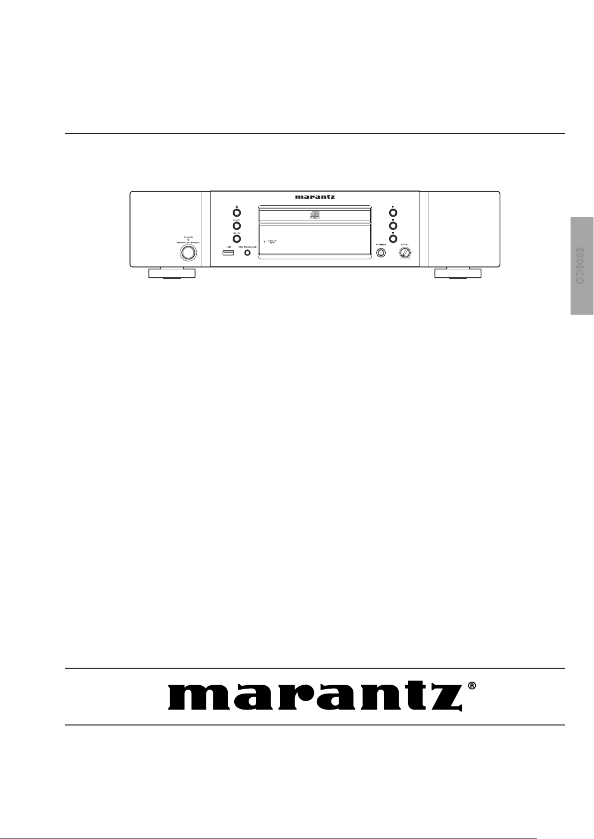
CD6003
CD6003 /
F N/K1SG/N1B/N1SG
Manual
SECTION PAGE
1. TECHNICAL SPECIFICATIONS............................................................................................1
2. SERVICE HINTS AND TOOLS .............................................................................................2
3. WARNING AND LASER SAFETY INSTRUCTIONS ............................................................3
4. TAKING THE DISC OUT OF EMERGENCY .........................................................................4
5. SERVICE MODE ...................................................................................................................4
6. ALL CLEAR ...........................................................................................................................8
7. ERROR MESSAGE ...............................................................................................................8
8. TROUBLESHOOTING .........................................................................................................20
9. UPDATE MICROPROCESSOR SOFTWARE PROCEDURE ............................................22
10. WIRING DIAGRAM ...............................................................................................................33
11. BLOCK DIAGRAM.................................................................................................................35
12. SCHEMATIC DIAGRAM .......................................................................................................37
13. PARTS LOCATION ...............................................................................................................43
14. EXPLODED VIEW AND PARTS LIST ..................................................................................53
15. MICROPROCESSOR AND IC DATA ....................................................................................57
16. ELECTRICAL PARTS LIST ...................................................................................................65
17. ABOUT REPLACE THE MICROPROCESSOR WITH A NEW ONE ....................................78
CD Player
TABLE OF CONTENTS
Please use this service manual with referring to the user guide (D.F.U.) without fail.
修理の際は、必ず取扱説明書を準備し操作方法を確認の上作業を行ってください。
CD6003
Part no. 90M23DW855010
First Issue 2009.06
ecm
Page 2
MARANTZ DESIGN AND SERVICE
USA
MARANTZ AMERICA, INC
100 CORPORATE DRIVE
MAHWAH, NEW JERSEY 07430
USA
EUROPE / TRADING
D&M EUROPE B. V.
P. O. BOX 8744, BUILDING SILVERPOINT
BEEMDSTRAAT 11, 5653 MA EINDHOVEN
THE NETHERLANDS
PHONE : +31 - 40 - 2507844
FAX : +31 - 40 - 2507860
KOREA
D&M SALES AND MARKETING KOREA LTD.
CHUNG JIN B/D., #1001,
53-5, WONHYORO 3 GA, YONGSAN-GU,
SEOUL, 140-719, KOREA
PHONE : +82 - 2 - 323 - 2155
FAX : +82 - 2 - 323 - 2154
CANADA
D&M Canada Inc.
5-505 APPLE CREEK BLVD.
MARKHAM, ONTARIO L3R 5B1
CANADA
PHONE : 905 - 415 - 9292
FAX : 905 - 475 - 4159
JAPAN
D&M BUILDING, 2-1 NISSHIN-CHO,
KAWASAKI-KU, KAWASAKI-SHI,
KANAGAWA, 210-8569 JAPAN
D&M Holdings Inc.
CHINA
D&M SALES AND MARKETING SHANGHAI LTD.
ROOM.808 SHANGHAI AIRPORT CITY TERMINAL
NO.1600 NANJING (WEST) ROAD, SHANGHAI,
CHINA. 200040
TEL : 021 - 6248 - 5151
FAX : 021 - 6248 - 4434
Using superior design and selected high grade components,
Only original
MARANTZ
parts can insure that your
MARANTZ
MARANTZ
company has created the ultimate in stereo sound.
product will continue to perform to the specications for
which it is famous.
Parts for your
MARANTZ
ORDERING PARTS :
equipment are generally available to our National Marantz Subsidiary or Agent.
Parts can be ordered either by mail or by Fax.. In both cases, the correct part number has to be specied.
The following information must be supplied to eliminate delays in processing your order :
1. Complete address
2. Complete part numbers and quantities required
3. Description of parts
4. Model number for which part is required
5. Way of shipment
6. Signature : any order form or Fax. must be signed, otherwise such part order will be considered as null and void.
NOTE ON SAFETY :
Symbol Fire or electrical shock hazard. Only original parts should be used to replaced any part marked with symbol .
Any other component substitution (other than original type), may increase risk of re or electrical shock hazard.
安全上の注意:
がついている部品は、安全上重要な部品です。必ず指定されている部品番号のものを使用して下さい。
SHOCK, FIRE HAZARD SERVICE TEST :
CAUTION : After servicing this appliance and prior to returning to customer, measure the resistance between either primary
AC cord connector pins (with unit NOT connected to AC mains and its Power switch ON), and the face or Front Panel of
product and controls and chassis bottom.
Any resistance measurement less than 1 Megohms should cause unit to be repaired or corrected before AC power is applied,
and veried before it is return to the user/customer.
Ref. UL Standard No. 60065.
In case of difculties, do not hesitate to contact the Technical
Department at above mentioned address.
080702MZ
Page 3
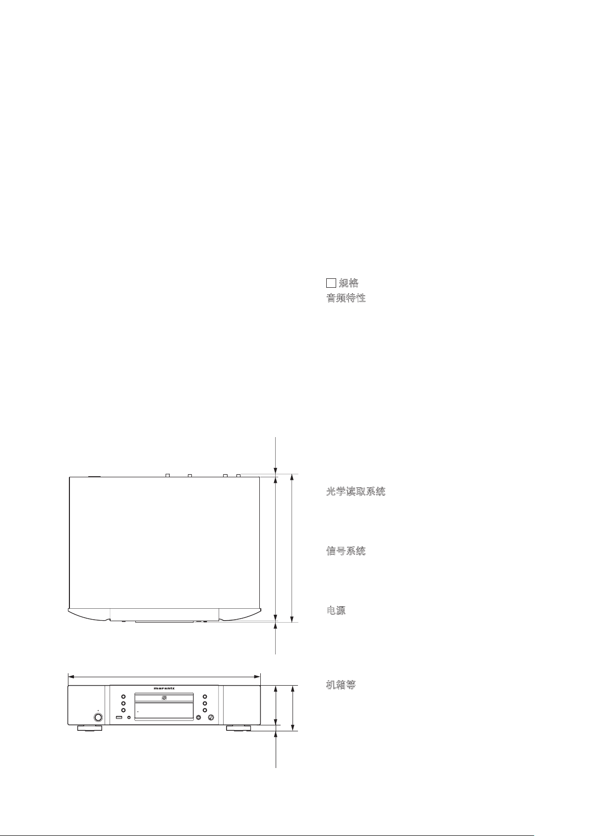
1. TECHNICAL SPECIFICATIONS
440 (17-3/8)
15.5 (5/8)
90.5 (3-5/8)
106 (4-3/16)
6.5 (5/16)4 (3/16)
339 (13-3/8)
328.5 (12-15/16)
Audio characteristics
Channels ...........................................................2 channels
Frequency response ....................................2 Hz to 20 kHz
Dynamic range ........................................................100 dB
Signal-to-noise ratio (A-weighted) ........................... 110 dB
Channel separation (1 kHz) ..................................... 110 dB
Harmonic distortion (1 kHz) ....................................0.002%
Wow & utter .........................................Precision of quartz
Audio output ..........................................2.35 V rms, stereo
Headphone output (variable maximum) ...18 mW/32 ohms
Digital output
Coaxial output (pin jack).....................0.5 Vp-p, 75 ohms
Optical output (square optical connector) ..........-19 dBm
Optical readout system
Laser...............................................AlGaAs semiconductor
Wavelength ............................................................. 780 nm
Dimensions (unit: mm)
Signal system
Sampling frequency .............................................. 44.1 kHz
Quantization ............................................16-bit linear PCM
Power supply
Power requirement ...............................AC 230 V 50/60 Hz
Power consumption ....................................................19 W
Standby power consumption .....................................0.3 W
█ 规格
[ K version only ]
音频特性
模拟输出 (载荷 =10kΩ Ref=1kHz)
.........................................................................
声道
频率响应
.........................
动态范围 (使用 FLP-A20k 时 )
信噪比 (使用 FLP-A20k 时 )
全频失真 (使用 FLP-A20k 时 )
.................................................................
晃抖度
输出水平
....................................................
数字输出
水平输出 (同轴 )
水平输出 (光学 )
.................................
.....................................
4Hz到 20kHz (Ref=0dB, ±3dB)
............
...................
...........
90dB (Ref=-60dB)
90dB (Ref=0dB)
0.008% (Ref=0dB)
2.35±0.3V rms
0.5V±0.1Vp-p,75Ω
-19 dBm ±3 dBm
2声道
石英精度
光学读取系统
........................................................
激光
...................................................................
波长
AlGaAs半导体激光
信号系统
采样频率
量化
...................................................................
...............................................................
电源
电源要求
功耗
待机电源消耗
.......................................................
................................................................................
..............................................................<
机箱等
允许的工作温度
允许的工作湿度
..................................................
........................................
5 ~ 90% (无结露 )
760 - 800nm
44.1kHz
16位线性 PCM
交流 220V 50Hz
19W
0.5W
+5 ~ +35
°C
1
Page 4
2
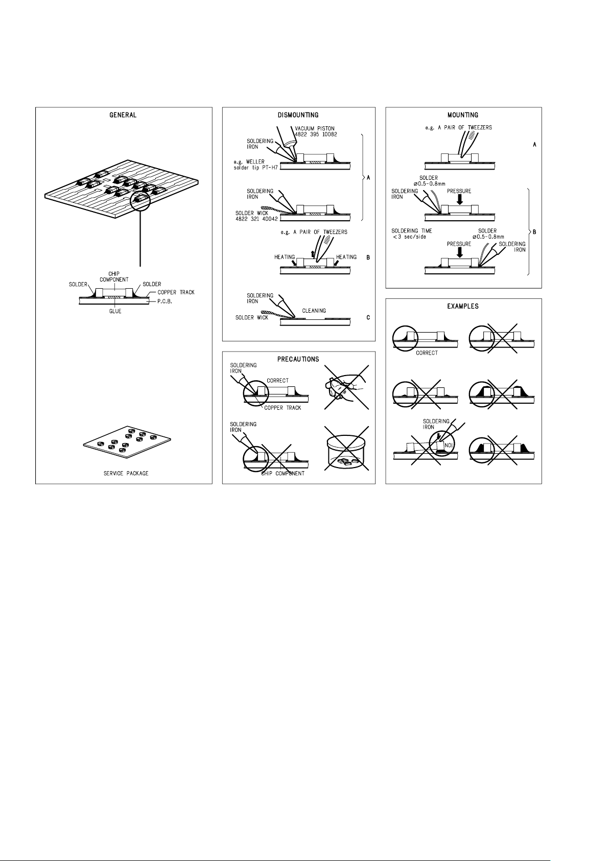
2. SERVICE HINTS AND TOOLS
DVD test disc (NTSC) ALMEDIO TDV-540
SERVICE TOOLS
Audio signals disc 4822 397 30184 or TCD-784
Disc without errors +
Disc with DO errors, black spots and fingerprints 4822 397 30245 (SBC444A) or TCD-726
Disc (65 min 1kHz) without no pause 4822 397 30155
Max. diameter disc (58.0 mm) 4822 397 60141
Torx screwdrivers
Set (straight) 4822 395 50145
Set (square) 4822 395 50132
13th order filter 4822 395 30204
DVD test disc (PAL) 4822 397 10131
SERVICE HIN
TS
070703MZ
Page 5
3
3. WARNING AND LASER SAFETY INSTRUCTIONS
F
ATTENTION
Tous les IC et beaucoup d’autres semiconducteurs sont sensibles aux décharges
statiques (ESD).
Leur longévité pourrait être considérablement
écourtée par le fait qu’aucune précaution
n’est prise a leur manipulation.
Lors de réparations, s’assurer de bien être
relié au même potentiel que la masse de
l’appareil et enfiler le bracelet serti d’une
résistance de sécurité.
Veiller a ce que les composa
nts ainsi que les
outils que l’on utilise soient également a ce
potentiel.
D
WARNUNG
Alle IC und viele andere Halbleiter sind
empfindlich gegen elektrostatische
Entladungen (ESD).
Unsorgfältige Behandlung bei der Reparatur
kann die Lebensdauer drastisch vermindern.
Sorgen sie dafür, das Sie im Reparaturfall
über ein Pulsarmband mit Widerstand mit
dem Massepotential des Gerätes verbunden
sind.
Halten Sie Bauteile und Hilfsmittel ebenfalls
auf diesem Potential.
WAARSCHUWING
Alle IC’s en vele andere halfgeleiders zijn
gevoelig voor elektrostatische ontladingen
(ESD).
Onzorgvuldig behandelen tijdens reparatie
kan de levensduur drastisch doen
verminderen.
Zorg ervoor dat u tijdens reparatie via een
polsband met weerstand verbonden bent met
hetzelfde potentiaal als de massa van het
apparaat.
Houd componenten en hulpmiddelen ook op
ditzelfde potentiaal.
AVVERTIMENTO
Tutti IC e parecchi semi-conduttori sono
sensibili alle scariche statiche (ESD).
La loro longevita potrebbe essere fortemente
ridatta in caso di non osservazione della piu
grande cauzione alla loro manipolazione.
Durante le riparazioni occorre quindi essere
collegato allo stesso potenziale che quello
della massa dell’apparecchio tramite un
braccialetto a resistenza.
Assicurarsi che i componenti e anche gli
utensili con quali si lavora s
iano anche a
questo potenziale.
All ICs and many other semi-conductors are
susceptible to electrostatic discharges (ESD).
Careless handling during repair can reduce
life drastically.
When repairing, make sure that you are
connected with the same potential as the
mass of the set via a wrist wrap with
resistance.
Keep components and tools also at this
potential.
WARNING
Safety regulations require that the set be restored to its original condition
and that parts which are identical with those specified be used.
Veiligheidsbepalingen vereisen, dat het apparaat in zijn oorspronkelijke
toestand wordt terug gebracht en dat onderdelen, identiek aan de
gespecifieerde worden toegepast.
Bei jeder Reparatur sind die geltenden Sicherheitsvorschriften zu beachten.
Der Originalzustand des Gerats darf nicht verandert werden
.
Fur Reparaturen sind Original-Ersatzteile zu verwenden.
Le norme di sicurezza esigono che l’apparecchio venga rimesso nelle
condizioni originali e che siano utilizzati pezzi di ricambiago idetici a quelli
specificati.
Les normes de sécurité exigent que l’appareil soit remis a l’état d’origine et
que soient utilisées les pièces de rechange identiques à celles spécifiées.
“Pour votre sécurité, ces documents
doivent être utilisés par des
spécialistes agrées, seuls habilités à
réparer votre appareil en panne.”
GB
NL
I
D
I
F
GB
NL
LASER SAFETY
CAUTION VISIBLE AND INVISIBLE LASER RADIATION WHEN OPEN AVOID EXPOSURE TO BEAM
ADVARSEL SYNLIG OG USYNLIG LASERSTRÅLING VED ÅBNING UNDGÅ UDS
Æ
TTELSE FOR STRÅLING
ADVARSEL SYNLIG OG USYNLIG LASERSTRÅLING NÅR DEKSEL Å PNES UNNGÅ EKSPONERING FOR STRÅLEN
VARNING SYNLIG OCH OSYNLIG LASERSTRÅLNING NÄR DENNA DEL ÄR ÖPPNAD BETRAKTA EJ STRÅLEN
VARO! AVATT AESSA OLET ALTTIINA NÄKYVÄLLE JA NÄKYMÄTTÖMÄLLE LASER SÄ
TEILYLLE. ÄLÄ KATSO SÄTEESEEN
VORSICHT SICHTBARE UND UNSICHTBARE LASERSTRAHLUNG WENN ABDECKUNG GEÖFFNET NICHT DEM STRAHL AUSSETSEN
DANGER VISIBLE AND INVISIBLE LASER RADIATION WHEN OPEN AVOID DIRECT EXPOSURE TO BEAM
ATTENTION RAYONNEMENT LASER VISIBLE ET INVISIBLE EN CAS D'OUVERTURE EXPOSITION DANGEREUSE AU FAISCEAU
USE OF CONTROLS OR ADJUSTMENTS OR PERFORMANCE OF PROCEDURE OTHER THAN THOSE
SPECIFIED HEREIN MAY RESULT IN HAZARDOUS RADIATION EXPOSURE.
AVOID
DIRECT EXPOSURE TO BEAM
WARNING
The use of optical instruments with this product will increase eye hazard.
Repair handling should take place as much as possible with a disc loaded inside the player
WARNING LOCATION: INSIDE ON LASER COVERSHIELD
This unit employs a laser. Only a qualified service person should remove the cover or attempt to service t
his
device,
due to possible eye injury.
030804ecm
Page 6
4
4. TAKING THE DISC OUT OF EMERGENCY
Model name is Displayed
モデル名表示
CD6003
“STOP”+“NEXT”+“POWER ON”
Version of Front microprocessor is
displayed
Fromtマイコンバージョン表示
Playback time displayed
再生時間表示
Playback time clear?
再生時間クリア確認
Turn on all segment
全点灯
NEXT PREVIOUS
PREVIOUS
Turn off all segment
全消灯
NEXT
Serial number is displayed
シリアル番号表示
Received command displayed
受信コマン ド表示
NEXT
Version of USB is displayed
USBバージョン表示
NEXT PREVIOUS
NEXT PREVIOUS
STOP(3sec)
NEXT PREVIOUS
NEXT PREVIOUS
PREVIOUS
Playback time clear
再生時間クリア
PREVIOUS
PLAY
①
②
③
⑥
⑦
④
⑤-a
⑤-b
⑧
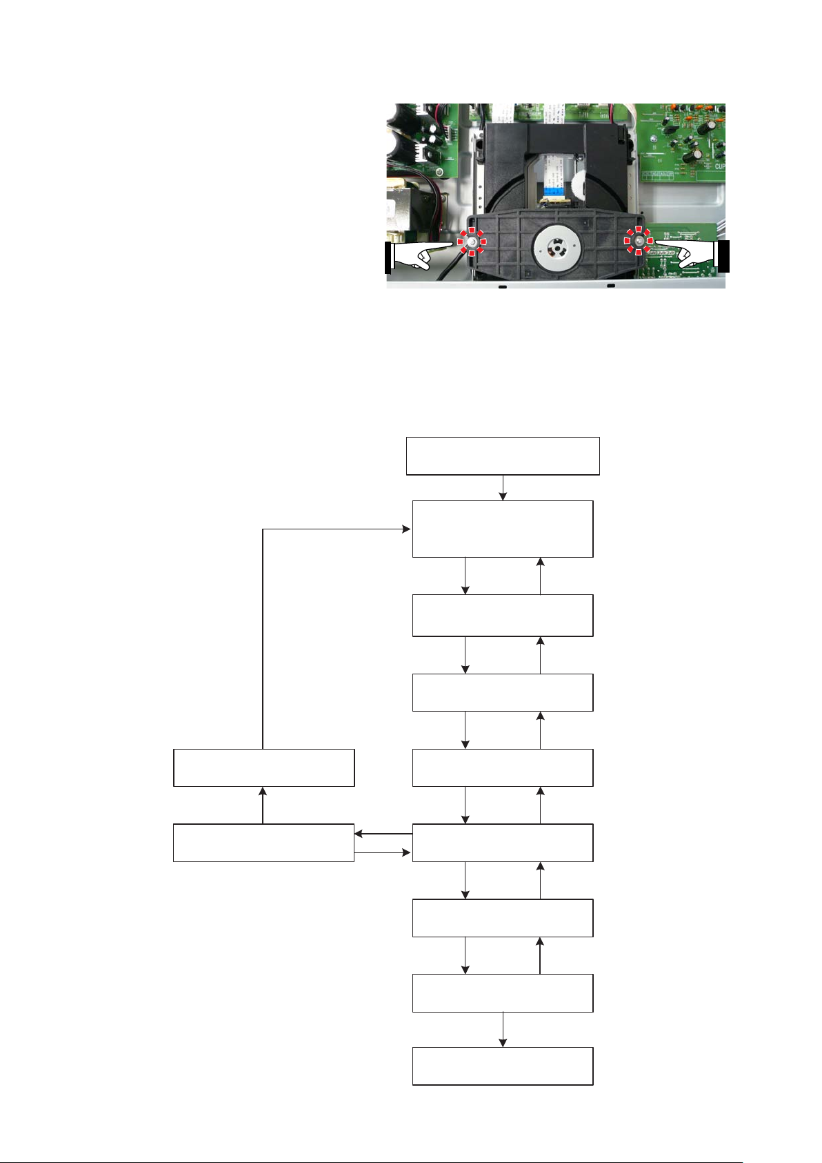
1. Remove the top cover of the player.
2. Remove 2 screws shown in the picture follows.
3. Remove the disc clamper.
4. Now you can remove the disc.
Remove those screws
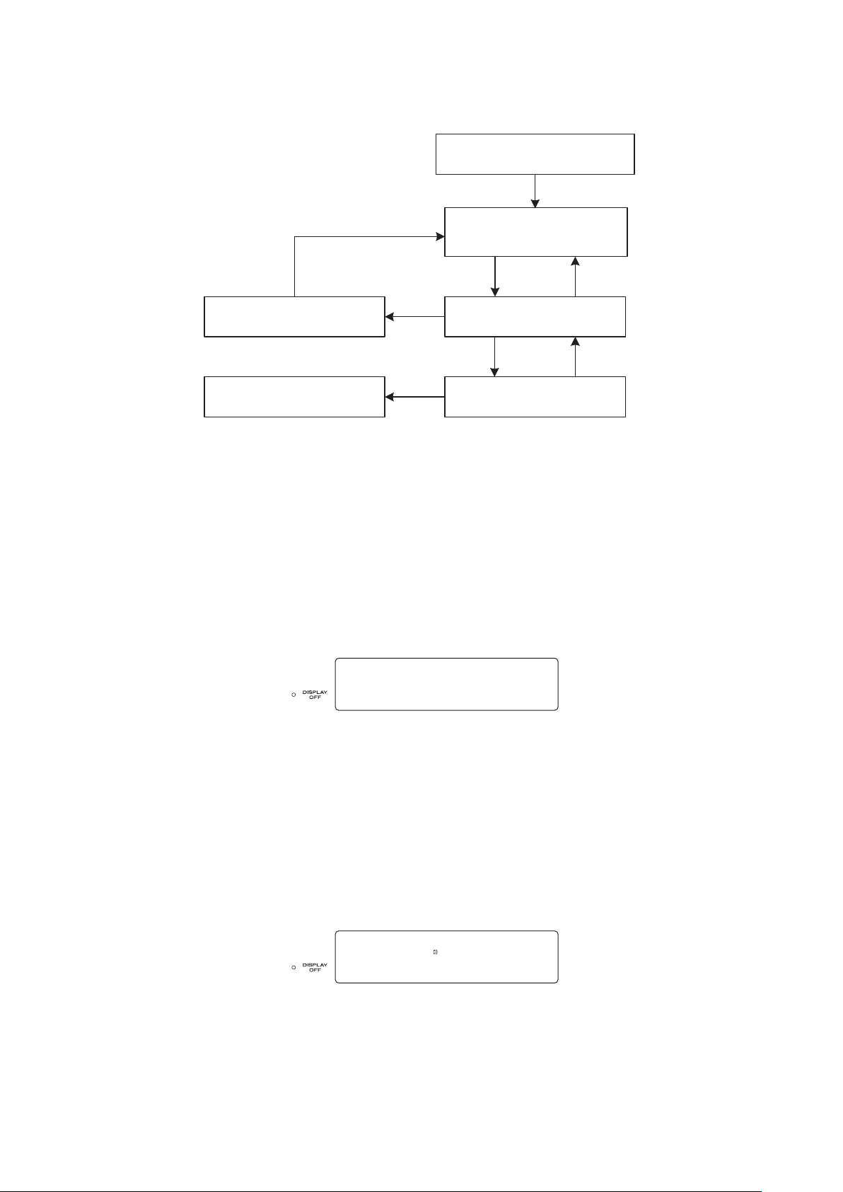
5. SERVICE MODE
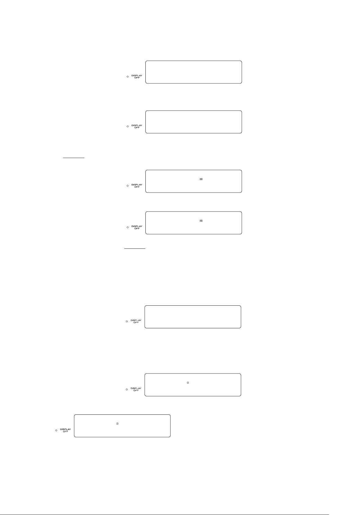
There are two modes in the service mode.
[A] Mode to display version information on each
module.
サービスモードには2種類あり、各モジュールのバージョン情報
を表示するモードとラストエラーメッセージを確認するモードがあ
ります。
[A] 各モジュールのバージョン情報等を表示するモード
Page 7
5
Here is the indication and specication of each function.
1. Model name is displayed.
以下に、それぞれの表示及び仕様を示します。
1. モデル名表示
モデル名をFLに表示します。
CD6003
2. Version of FRONT microprocessor is displayed.
FRyyyymmddxx
3. Version of USB device is displayed.
First, Revision of USB device is displayed.
u P D 6 3 9 0 1 3 0 1
Press NEXT button, then version of USB is displayed.
U V e r : V . 1 0 2
Push PREVIOUS button then Revision of USB device
is displayed.
Revision of USB is display of LSI when the PREVIOUS
button is pushed when light up all FL segment.
2. Frontマイコンバージョン表示
フロントマイコンのバージョン表示を行います。
3. USBバージョン表示
USBデバイスのバージョン情報を表示します。
まず、LSIのデバイスのリビジョンを表示します。
NEXT
キーが押されるとバージョン情報を表示します。
PREVIOUS
します。
又、全点灯表示を行っている際、
ると、LSIのリビジョン表示に復帰します。
キーが押されるとLSIのリビジョン表示に復帰
PREVIOUS
キーが押され
4. Serial number is displayed.
5-a. CD playback time is displayed.
It is only a HOUR display.
To be displayed backup time , press PLA Y button.
BTime:xxxxxh
To be displayed playback time, press PUSE button.
4. シリアル番号表示
シリアル番号の表示を行います。
MZ xxxxxxxxx
5-a. 再生時間表示
CD及びSA-CDのそれぞれの再生時間を表示します。
再生時間は、分秒の表示は行わないものとします。但し、
再生時間のカウンタは秒単位でカウントを行っています。
PTime:xxxxxh
再生時間を表示中に
プされた再生時間を表示します。これは、CDモ
交換した際、次項の再生時間クリアを行いますが、その時に
交換する前の CDモジュールの再生時間をメモリにバック
アップし、その情報を確認することが可能です。
PAUSE
します。
PLAY
キーが入力される
キーが入力されると、現在の再生時間表示に復帰
と、バックアッ
ジュールを
Page 8
6
5-b. Confirmation of to do clear playback time
When replacing SUPER AUDIO CD module and reset
playback times.
Press the STOP button more than 3 seconds while
playback time is displayed.
PTime Clear?
5-b. 再生時間クリア確認
CDモジュールを交換した場合、再生時間をクリアする必要
があります。
再生時間表示中に
間クリア確認表示に移行します。
STOP
キーを3秒以上長押しで再生時
Press PLAY Button.
Done : xxx
xxx : number of changed CD module
The display is as follows.
PTime:00000h
Press the PREVIOUS button while conrmation of to do
clear playback time.
6. Light up all FL segment
The icon and the character representation are displayed
every second. Standby LED doesn’t light.
この表示中に
す。再生時間がクリアされると以下の表示に切り替わります。
ここで、表示中のxxxはCDモジュールの交換履歴になりま
す。この表示を約3秒間表示行うと再生時間がクリアされ
たことを示すために以下の表示を行います。
再生時間クリア確認表示中に
と再生時間表示に復帰します。
6. 全点灯
使用する部品が全点灯を禁止としているため、ICON部と文
字表示部を1秒毎に交互に表示させます。
但し、Standby LEDに関しては、Standby機能と連動して
いるため、全点灯時にも点灯することはありません。
PLAY
キーを押すと再生時間がクリアされま
PREVIOUS
キーが押される
7. Light off all FL segment
8. Confirmation of remote control command
The command input by a key and a remote controller is
displayed.
When the STANDBY button is pressed or Standby RC
code is received, it shifts to Standby.
7. 全消灯
8. 受信
全ての表示を
コマンド表示
フロントにあるキー及びリモートコントローラーから入力され
るコマンドを表示部に表示します。
但し、
ます。同様にリモートコントローラーよりPower OFF及び
Power On/Offコマンドを受信した場合もStandbyに移行
します。
消灯します。
STANDBY
キーが押された場合 Standbyに移 行し
Page 9
7
[B] The mode to check the last error message etc.
Error rate
エラーレート
PLAY
Model name is displayed
モデル名表示
CD6003
“STOP”+“NEXT”+“POWER ON”
PREVIOUSSTOP
Execution
実行
Message of last error
ラストエラーメッセージ
PREVIOUSSTOP
STOP(3s)
Clear
This test mode is common to all models.
[B] ラストエラーメッセージなどを確認するモード
このテスト用のモードは全てのモデルにおいて共通仕様です。
Here is the indication and specication of each function.
1. Last Error Message
This function enables the users to check error messages
at a later time when an error has occurred between the
front microprocessor and each device.
However, it does not display all errors. For more
information about what messages can be displayed, refer
to the Other Error Message page.
When no error has ever occurred, it displays the
following.
No Error
Hold the STOP button for 3 seconds while the last error
message is being displayed, and the last error message
will be cleared. After the last error message is cleared,
the model identication returns to the display.
2. Error Rate
This function determines the CD error rate. When the disk
that can be reproduced has been inserted, it displays it as
follows. Here, the case where CD-DA has been inserted
is indicated.
ここで、それぞれの表示及び仕様を示します。
1. ラストエラーメッセージ
フロントマイコンと各デバイス間の通信エラーなどが生じた
際のエラー表示を、後からでも確認できる機能です。
但し、全てのエラー表示を記録するわけではありません。
表示が可能なエラー情報はエラーメッセージの項を参照く
ださい。
尚、エラー情報がない場合は、以下の表示を行います。
ラストエラーメッセージを表示中に、
STOP
キーを3秒間押
し続けるとラストエラーメッセージ情報をクリアすることがで
きます。このとき、ラストエラーメッセージ情報のクリアが完
了するとモデル名表示に自動的に復帰します。
2. エラーレート
CDのエラーレートを測定します。
再生可能なディスクが挿入されていると以下の表示を行い
ます。ここでは、CD-DAが
挿入されている場合を示します。
C1/C2 Count?
The measurement of the error rate of inserted disk
and real machine begins when Play Key or remote
controller's Play command is input while displaying the
above-mentioned.
The error rate displays the sum total of the C1 error and
the C2 error every one second with Hex.
上記表示中にPlay Key又はリモートコントローラーのPlay
コマンドが入力されると、挿 入されたディスクと実機のエ
ラーレートの測定を開始します。
エラーレートは、1秒毎のC1エラー及び C2エラーの総和を
Hexで表示します。
Page 10
8
The example of the display is for your information
shown.
C1002AC2000F
参考までに表示例を示します。
Four digits since C1 are the C1 errors. Four digits since
C2 become the C2 errors. The buttons that function or
command becomes Stop, Open/Close, Standby, Power,
and Power Off while measuring it.
The buttons that function while this message is being
displayed are OPEN/CLOSE and PLAY.
6. ALL CLEAR
To reset the back up memory of the unit into the default
status, follow the procedure below.
However, information of the serial number and the
reproduction time on the set cannot be deleted by this
function. Connect the mains cord into the unit and press
STOP and POWER ON button simultaneously more than
3 seconds.
6. オールクリア
Reset
ここで、C1以降の4桁がC1エラーの値となり、C2以降の4
桁が C2エラーの値となります。
測定中に有効なKey又はコマンドは、Stop、Open/Close、
Standby、Power及びPower Offとなります。
この表示中に有効なキーはOPEN/CLOSEとPLAYになり
ます。又、同じディスクを使用しても同じ値が出るとは限り
ません。
本機能を使用することで、工場出荷状態の設定に戻すこと
が可能です。但し、セットのシリアル番号及び再生時間情
報に関しては本機能で消去することはできません。
STOP
キーを押した状態で
Standby解除から3秒間
ルクリアに移行します。オールクリアの状態に移行すると、
以下の表示に変わります。
POWER ON
STOP
キーが押され続けるとオー
キーを押します。
"Reset" is displayed, after "Reset OK" displayed on
the display 3 seconds, then unit returns to the normal
status.
Reset OK
7. ERROR MESSAGE
The error message common to all models.
[A] The error message displayed as the Last Error
Message
1 Peculiar error information to CD module
1) Limit switch error of pick up
The CD module moves picking up to an inner side and
the outer side when starting, and conrms whether the
switch that exists in the CD module works normally. At this
time, when the switch that provides for range of motion
on an inner side of picking up doesn't work normally, the
following errors are displayed.
オールクリアの処理が完了すると以下の表示を3秒間表示
し、通常状態の表示に復帰します。
7. エラーメッセージ
全モデル共通のエラーメッセージ
[A] ラストエラーメッセージにて表示されるエラーメッセージ
1 CDモジュール単独のエラー情報
1) ピックアップのリミットスイッチエラー
CDモジュールは起動時にピックアップを内周側と外周側に
移動して、CDモジュールにあるスイッチが正常に動作して
いるか確認を行います。この時、ピックアップの内周側の動
作範囲を規定するスイッチが正常に動作していない場合、
以下のエラーを表示します。
CDLimitSWErr
At this time, please conrm whether the tray open/close
rst pressing the OPEN/CLOSE button.
Please refer to "The tray do not Open/Close" when it is
not possible open or close.
この時、まず
クローズするか確認してください。
オープン/ クローズできない場合は、“トレイがOpen/Close
できない”を参照ください。
OPEN/CLOSE
キーを押してトレイがオープン /
Page 11
9
Conrm whether pick-up operates on a reception desk
side and a rear side when opening/closing when a
pertinent error is conrmed to can open/close.
Conrm each cable when it doesn't operate or the voltage
of 1pin and 2pin of CN32 changes from 7.5V into about
4V. Conrm the solder of IC21 and CN32 when having
changed. There is a possibility of the breakdown of the
CD module when not having changed. Exchange CD
modules.
オープン/クローズができるのに該当エラーが確認される場
合は、オープン/ クローズした際にピックアップ本体がフロン
ト側及びリア側に動作しているか確認してください。
動作していない場合、CN32の1pin及び2pinの電圧が7.5V
から4V程度に変化する場合は、各ケーブルを確認してくだ
さい。動作している場合は、CN32の 6pinがトレイをクロー
ズした際にHigh⇔ Lowと変化するか確認してください。
変化している場合はIC21及び CN32の半田を確認してく
ださい。 変化していない場合、CDモジュールの故障の可
能性があります。CDモジュールを交換してください。
2) Transfer error of boot program of CD DSP
The following error of three is divided in the software
debug. It displays it to CD DSP when failing in writing the
boot program. In this case, conrm the solder of IC31 of
CUP12190x. If the same problem arises after conrmed,
IC31 may be broken. If such is the case, replace IC31.
PRAM ACK E r r
PRAM Cal Err
PRAM Sum E r r
3) Error concerning discs
When the disk cannot be read by some reasons in
the disk relation, the following displays are done. The
condition, when it takes 60 seconds or more to read
TOC of the disk and CD-DA not being done for the disk
and write from be not shut session (CD-I) and the rst
session that focus doesn't encounter it that cannot be
reproduced or it takes 120 seconds or more to analyze
CD-ROM, it displays it.
2) CD DSPのブートプログラムの転送エラー
下記の 3つのエラーに関しては、ソフトウェアのデバック上
分けていますが、CD DSPへブートプログラムの書き込みに
失敗した場
のIC31の
確認後も同様のエラーが表示される場合、IC31の故障の
可能性があります。IC31を交換してください。
3) ディスク関連のエラー
ディスク関連で、何らかの理由でディスクが読めない場合以
下の表示を行います。
条件的には、フォーカスがあわない、再生不可能なセッショ
ン(CD-I)、最初のセッションが閉じられていないディスク、書
き込みがされていないディスク、CD-DAの TOCの読み込み
に60秒以上かかる場合、CD-ROMの解析に 120秒以上か
かる場合に表示を行います。
合に表示を行います。この場合、CUP12190x
半田を確認してください。
Can't Play
When the acquisition of information that is called subcode
Q data including information of TOC information and the
reproduction time cannot be acquired longer than the
xed time, this display is displayed. There is a possibility
that there are some problems on the disk side when a
general disk can be reproduced, and only a specic
disk is displayed. There is a possibility that IC31, IC32
or the CD module is out of order when the error of the
correspondence occurs on not a specic disk but two or
more disks.
SubQ Error
この表示は、TOC情報や再生時間情報を含むサブコードQ
データと呼ばれる情報の取得が一定時間以上取得できな
かった場合に表示されます。
一般のディスクが再生できていて、特定のディスクのみ表示
される場合はディスク側に何らかの問題がある可能性があ
ります。
特定のディスクではなく複数のディスクで該当のエラーが発
生する場合、IC31
可能性があります。CDモジュールを交換してみても該当エ
ラーが発生する場合はIC31又はIC32を交換してください。
、IC32又はCDモジュールが故障している
Page 12
10
When the error is continuously caused ve times or
more, two or more errors do the following display by
internal processing. There is a possibility that IC31, IC32
or the CD module is out of order when the error of the
correspondence occurs on not a specic disk but two or
more disks. Exchange IC31 or IC32 when a pertinent
error occurs even if CD modules are exchanged.
ErrCountOver
内部処理で複数のエラーが連続で5回以上エラーが生じた
場合に下記の表示を行います。
特定のディスクではなく複数のディスクで該当のエラーが発
生する場合、IC31、IC32又はCDモジュールが故障している
可能性があります。
CDモジュールを交換してみても該当エラーが発生する場
合はIC31又はIC32を交換してください。
4) Communication Error between D/A Converter and
Front Microprocessor
If no response is detected in the communication between
the D/A Converter and the Microprocessor, the display
will show the following message.
Check that the exible cable has been duly connected
between CUP12190x and CUP12192x and also that
L752(+5V) and IC75(14pin(+3.3V))on theCUP12192x
are receiving the designated voltage.
Make the CD or the USB repayable.
Ensure that IIC communications have been established
between R755 and R756 when the unit is switched from
STOP to PLAY.
If the error cannot be corrected through normal operations,
IC75 may be broken. If such is the case, replace IC75.
DACErrorIIC
5) iPod-authenticated error and the microprocessor
communication error
If no response is made in the communication with an
iPod-authenticated IC within a regulated timeframe, the
display will show the following message.
As the communication with the authenticated IC has not
been established normally, ensure that the IIC signal
is communicating at a normal level when the unit is
connected with an iPod.
The frequency of the IIC clock (IIC_SCL) is approximately
40 kHz only when the unit communicates with an iPodauthenticated IC. If no communication can be detected,
check the soldering points of the microprocessor (IC21
on CUP12190x), resistors (R214, R215, R217 and R218
on CUP12190x) and the authenticated IC (R214 on
CUP12190x).
If the problem specic to the iPod cannot be rectied, the
authenticated IC (IC27 on CUP12190x) may be broken.
If that is the case, replace IC27.
4) D/Aコンバータとマイコンとの通信エラー
D/Aコンバータとマイコンの通信において指定時間内に応
答がない場合、以下の表示を行います。
CUP12190xとCUP12192xを接続しているケーブルがき
ちんと接続されているか確認してください。
CUP12192x上 の L752(+5V)と IC75 の 14pin(+3.3V)を
確認し、指定の電圧か確認してください。
CD又はUSBを再生可能な状態にしてください。
St
op状 態からPlay状
にIIC通信が行われているか確認してください。
通常動作が行われている状態で、当エラーが解消できない
場合、IC75が壊れている可能性があります。IC75を交換し
てください。
5) iPodの認証ICとマイコンの通信エラー
iPodの認証 ICとの通信において指定時間内に応答がない
場合、以下の表示を行います。
認 証 ICとの通 信が正 常に行われていない状態なので、
iPodを接続したときにIICの信号が正常なレベルで通信し
ているか確認してください。
尚、iPodの認証 ICとの通信を行うときのみIICのクロック
(IPOD_SCL)は約 40kHzになります。 通信が行われてい
ないようであれば、マイコン(CUP12190x上のIC21)、抵
抗(CUP12190x上の R214、R215、R217、R218)、認証
IC(CUP12190x上の IC27)の半田付けの状態を確認して
ください。
通常動作が問題なくiPodの
は、認証 IC(CUP12190x上のIC27)が壊れている可能性
があります。IC27を交換してください。
態に変更するときに R755とR756
みの問題が解決できない場合
iPodErrorIIC
Page 13
11
6) Other errors of iPod-authenticated error
When the iPod-authenticated IC has received error
information, the display will show the following message.
This message means that the authenticated IC is
communicating properly. Try connecting another iPod.
If no problem arises with another iPod, advise the user
to repair the iPod.
If the same problem arises with another iPod, the
authenticated IC (IC27 on CUP12190x) may be broken.
If that is the case, replace IC27.
iPodICErrorx
6) 認証 ICのその他のエラー
iPodの認証 IC上で確認できる認証エラーの情報を受け取
ると以下の表示を行います。
この表示の場合、認証 ICとの通信は正常に行われている
ので、他の iPodを接続してみてください。
他のiPodを接続して問題がないようであれば、iPod側の修
理をするよう勧めてください。
他の iPodでも同 様のエラー 表 示が出る場 合、認 証
IC(CUP12190x上の IC27)が壊れている可能 性がありま
す。IC27を交換してください。
When a problem arises with the processing of the iPod
authentication and signature, the display will show the
following message.
If the following message appears instead of the above
messages - "iPodErrorIC”, "iPodICErrorx" and "USB_
Com_Error_", try connecting another iPod.
If no problem arises, advise the user to repair the iPod.
If the error message persists, the authenticated IC (IC27
on CUP12190x) may be broken. If that is the case,
replace IC27.
ErrAuthentic
2 Error Messages special to USB device
If no response is made in the communication between
the USB Module and the microprocessor within a
designated timeframe, the display will show the following
message.
Ensure that each of L161, L251, L252 and L181 on
CUP12190x is applied with the voltage.
Ensure that each of 1pin and 50pin in IC11 on
CUP12190x is supplied with the clock signal of the
designated frequency.
Check the soldering points of IC21, IC11 and arround.
Refer to the Communication between USB Module and
the microprocessor on the Communication Waveform
page and check the signal.
If the error message bellow cannot be cleared despite
the unit performing normal operations properly, IC11 may
be broken. If such is the case, replace IC11.
iPodの認証及び署名に関する処理に問題が発生すると、以
下の表示を行います。
上の“iPodErrorIC”、“iPodICErrorx”及び“USB_Com_
Error_”が表示されなくて以下の表示がされる場合、他の
iPodを接続してみてください。
他のiPodを接続して問題がないようであれば、iPod側
理をするよう勧めてください。
他の iPodでも同 様のエラー 表 示が出る場 合、認 証
IC(CUP12190x上の IC27)が壊れている可能 性がありま
す。IC27を交換してください。
2 USBデバイス単独のエラー情報
USBデバイスとマイコンの通信において指定時 間内に応
答がない場合、以下の表示を行います。
CUP12190xの L161、L251、L252及び L181にそれぞれ
の電圧が印加されているか確認してください。
CUP12190xの IC11の 1pin及び 50pinに所 定の周 波 数
のクロック信号が見えるか確認してください。
IC21とIC11及び周辺回路の半田付けの状態を確認してく
ださい。
通信 波形の項にあるUSBデバイスとマイコンとの通信を
参照し、その信号を確認してください。
通常動作が問題なく下記エラーメッセージが解消できない
場合は、IC11が壊れている可能性があります。IC11を交換
してください。
の修
USB Com Err
Page 14
12
[B] Error messages that are not displayed in the
Last Error Message
1 Error messages that can be displayed on the FL or
LCD
1) Communication Error between the Front
Microprocessor and EEPROM
If no response is detected between the Front Microprocessor
and EEPROM within a regulated timeframe, the display
will show the following message.
Ensure that IIC communications have been established
between R235 and R236 on CUP12190x when the unit
is powered on or put into STANDBY.
If no communication is detected, check the soldering of
R212, R213, R235, R236, IC21 and IC22.
IF the error cannot be corrected through normal
operations, IC22 may be broke. If such is the case,
replace IC22.
EROMErrorIIC
[B]
ラストエラーメッセージにて表示されないエラーメッセージ
1 FL又はLCD上に表示可能なエラーメッセージ
1) マイコンとEEPROMとの通信エラー
EEPROMとマイコンの通信において指定時間内に応答が
ない場合、以下の表示を行います。
電 源 投 入 時 又はスタンバイ移 行 時に、CUP12190xの
R235とR236に IIC通信が行われているか確認してくださ
い。
通信が行われていない場合、R212、R213、R235、R236、
IC21、IC22の半田の状態を確認してください。
通常動作が行われている状態で、当エラーが解消できない
場合、IC22が壊れている可能性があります。
IC22を交換してください。
2) Error Messages special to USB
If no response is made while the unit is communicating
with the USB Module, the display will show the following
message.
If the indication will not be changed to "USB_Com_Err",
the communication may be unstable. Check if the
regulated voltage is applied to each of L161, L251 and
L252 on CUP12190x.
Check if 1pin and 50pin in IC11 on CUP12190x receive
the clock signal of the designated frequency
Check the soldering points of IC21, IC11and around.
Refer to the communication between the USB module and
the microprocessor on the communication waveform
page and check the signal. If the message below cannot
be cleared while the unit is functioning normally, IC11 may
be broken. If that is the case, replace IC11.
USBERR:EF:xx
When the unit is connected with an incompatible UBS
device or a device configured with an incompatible
communication protocol or command, the display will
show the following message.
If this message is displayed, the device is incompatible
and cannot be connected to the unit.
2) USB単独のエラー情報
USBデバイスに通信を行った際に、USBデバイスから返答
がない場合、以下の表示を行います。
“USB_Com_Err
ている可能性があります。
CUP12190xの L161、L251、L252及び L181にそれぞれ
の電圧が印加されているか確認してください。
CUP12190xの IC11の 1pin及び 50pinに所 定の周 波 数
のクロック信号が見えるか確認してください。
IC21とIC11及び周辺回路の半田付けの状態を確認してく
ださい。
通信 波形の項にあるUSBデバイスとマイコンとの通信を
参照し、その信号を確認してください。
通常動作が問題なく下記エラーメッセージが解消できない
場合は、IC11が壊れている可能性があります。IC11を交換
してください。
接続されたUSB機器が対象 外のもの( 例えばUSBキー
ボードなど)や、本機で対応できない通信プロトコルやコマン
ドを使用している機器が接続された場合、以下の表示を行
います。
本表示が行われた機器は、本機対象外の機器のため接続
はできません。
”に移行しない場合、通信が不安定になっ
Can'tConnect
If the information obtained from the USB has a aw or
improper data, which are detected by the USB host
controller in the unit, the display will show the following
message.
接続されたUSBか
タがある場合、通信のタイムアウト及び本機で使用している
USBのホストコントローラーがエラーを検出すると以下の表
示を行います。
ら取得した情報に不具合や不正なデー
Page 15
13
When the message appears, the device may be
connected and used, but success is not guaranteed.
ConnectError
この表示が行われた機器に関しては、場合によっては接続
ができるかもしれませんが、接続に関しては、保障するもの
ではありません。
If the signal comes in an incompatible format, the display
will show the following message.
The compatible formats are FAT16 and FAT32. In FAT32
the USB memory must be 128MB or bigger in size.
Moreover, it doesn't correspond to the le system for
usual Mac OS when formatting it with Mac OS of the
Apple Co.. Please format it with FAT32. (OS supports it
up to 32GB or less. )
FAT Error
This message means that the device is formatted in
an incompatible cluster size. Normally, when USB
memories are formatted on Microsoft Windows, FAT32
is the default, and if the memory size is up to 128MB,
it will be formatted in a cluster size of 2KB, which is
incompatible with the unit. Therefore, the memory size
is recommended to be 256MB or bigger. If the memory
size is 128MB, format it with FAT16 (indicated as FAT
on Microsoft Windows) instead of FAT32, and it will be
compatible with the unit.
本機で対応できない規格でフォーマットされている場合、以
下の表示を行います。
本 機で対 応 可 能なファイルフォーマットは、FAT16又は
FAT32になります。 但し、FAT32の場 合 128MBより大き
なUSBメモリに限ります。又、Apple社のMac OSでフォー
マットする場合は、通常の Mac OS用のファイルシステムに
は対応していません。FAT32でフォーマットするようにして
ください。(最大 32GBまでOSがサポートしています。)
本機で対応できないクラスタサイズでフォーマットされてい
ます。 通 常 Microsoft Windowsで USBメモリ等をフォー
マットする場合、FAT32がデフォルト設 定になっていま
そのため、128MBま
応できない2kBのクラスタを使用してフォーマットされてし
まいます。よって、256MB以上のメモリを推奨しています。
128MBの USBメモリを使用する場合、FAT32でフォーマッ
トするのではなくFAT16(Microsoft Windows上では FAT
と表記されます)でフォーマットすると、本機で使用すること
ができるようになります。
でのサイズのメモリの場合、本機で対
す。
Cluster Err
If the unit receives a power supply exceeding the
maximum level (500 mA) via USB, the display will show
the following message and the power supply will be
cut off. If the message below appears, the USB device
cannot be operated through the unit’s USB Bus power
alone. An auxiliary power unit might enable the device
to be used, but damage resulting from this would not be
covered by the warranty.
OverCurrent
If the command will not be set within a set timeframe
after PLAY, PAUSE, STOP, FF, FR and such operations
are carried out, the display will show the following
message.
This message will be displayed for 3 seconds and then
the USB module will be reset.
If the error indication persists after these operations,
IC11 may be broken as the unit will not accept a specic
command alone. If no other error message will appear,
replace IC11.
USBを介して本機で供給可能な電流 値の制 限 (500mA)
を超えた場合、以下の表示を行い、電源供給を中止します。
この表示が現れる機器を本機のみの USBバスパワーで動
作することはできません。 補助電源にて供給可能なUSB
デバイスの場合は使用できる場合もありますが、本機での
動作保障外となります。
USBデバイスに対してファイルの再生、一時停止、停止、早
送り、早戻しといった操作を行った際に、一定時間たっても
コマンド設定が行われない場合
この表示に関しては、3秒間表示した後USBデバイスに対
してリセットをかけます。
同様の動作を行ってもエラー表示が現れる場合、特定コマ
ンドのみ受け付けていないためIC11が壊れている可能性が
あります。他のエラー表示が確認できない場合、IC11を交
換してください。
に、以下の表示を行います。
USB Time Out
Page 16
14
If the le has an incompatible extension or is 24KB
or smaller in size, the display will show the following
message.
Extensions other than those mentioned in the instructions
manual will be excluded from the warranty. Refer to the
instructions manual and ensure that the extension and
format is compatible with the unit.
File Error
本機で再生できない拡張子のファイルや24kB以下のファ
イルの場合、以下の表示を行います。
取扱説明書に記載されている拡張子以外は、対象外又は
保障外となります。
取扱説明書に記載されている拡張子で対象フォーマットの
ファイルを利用してください。
If the unit detects an incompatible sampling frequency
or number of channels or an incompatible format le, the
display will show the following message.
Sampling frequencies, numbers of channels and formats
other than those mentioned in the instructions manual will
be excluded from the warranty. Refer to the instructions
manual and ensure that the format is incompatible.
Header Error
If the le includes big sized image data or information, the
analysis may take time. If the analysis takes more than 15
seconds, the display will show the following message.
If this message appears, the operation of the le will not
be covered by the warranty.
Time Out
If the USB module turns off the command for the settings
of AMS, Repeat or Random, the display will show the
following message.
If the error persists after the mode is switched to Disc
from USB and then reswitched to USB and the designated
remote control code is sent, IC11 may be broken as it will
not accept a specic command alone. If no other error
message appears, replace IC11.
本機で再生できないサンプリング周波数やチャンネル数、未
対応のフォーマットのファイルを検出すると以下の表示を行
います。
取扱説明書に記載されているサンプリング周波数、チャンネ
ル数及び対応フォーマット以外は、対象外又は保障外となり
ます。取扱説明書に記載されている対象フォーマットのファ
イルを利用してください。
サイズの大きな画像データや情報が付加されている場合、
その情報の解析に時間がかかることがあります。
本機では、解析時間が15秒以上かかる場合に以下の表示
を行います。この表示がでるファイルの再生に関しては、保
障外
となります。
AMS設定、Repeat設定、ランダム設定等の要求に対して
USBデバイスがコマンドを無効と処理した場合、以下の表
示を行います。
一旦USBモードからDiscモードに切り替えた後、再度 USB
モードに戻して、該当のリモコンコードを送付しても同様の
エラーが出る場合、特定コマンドのみ受け付けていないため
IC11が壊れている可能性があります。他のエラー表示が
確認できない場合、IC11を交換してください。
xh Mode Err
If the USB module turns off the command for setting AMS,
Repeat or Random and specifying the range, the display
will show the following message.
If the error persists after the mode is switched to Disc
from USB and then reswitched to USB and the designated
remote control code is sent, IC11 may be broken as it will
not accept a specic command alone. If no other error
message appears, replace IC11.
Range Error
AMS設定、Repeat設定、ランダム設定等の要求に対して
USBデバイスが各動作を行う範囲指定に対して無効と処
理した場合、以下の表示を行います。
一旦USBモードからDiscモードに切り替えた後、再度 USB
モードに戻して、該当のリモコンコードを送付しても同様の
エラーが出る場合、特定コマンドのみ受け付けていないため
IC11が壊れている可能性があります。他のエラー表示が
確認できない場合、IC11を交換してください。
Page 17
15
When the unit has failed to search for a folder or a le,
obtain folder information or set the default, the display
will show the following message.
If this error repeats, IC11 may be broken. If that is the
case, replace IC11.
Setup Error
フォルダ及びファイルの検索、フォルダの情報の取得、デフォ
ルト設定時等に失敗した際に、以下の表示を行います。
何度もこのエラーが確認される場合、IC11が壊れている可
能性があります。IC11を交換してください。
If the unit has failed to obtain information of the le
to be played back, the display will show the following
message.
If this error occurs to a specic le, the le information
may be corrupted. Check the le header and other
information.
If the error occurs to all les, IC11 may be broken. If no
other error message appears, replace IC11.
xxh Error
If the unit has failed to obtain information of the SB
manufacturer, the product and the serial number, the
display will show the following message.
On the display, the "x" will be replaced by the number 1,
2 or Failed to obtain manufacturer information; 2. Failed
to obtain product information; 3. Failed to obtain serial
number.
If this message appears, use of the device will not be
covered by the warranty.
再生対象ファイルの情報の取得に失敗すると以下の表示
を行います。
特定のファイルでこのエラーが確認される場合、そのファイ
ルの情報が壊れている可能性があります。
ファイルのヘッダ情報等を確認してください。
全てのファイルに対してこのエラーが確認される場合、IC11
が壊れている可能性があります。 他のエラー表示が確認で
きない場合、IC11を交換してください。
USBの製造者情報、製品情報及びシリアル情報の取得に
失敗すると、以下の表示を行います。
表示上の“x”は、1~ 3の数字が表示され、1:製造者情報
の取得に失敗、2:製品情報の取得に失敗、3:シ
の取得に失敗を示します。
本表示が現われた機器は、本機で接続及び動作を保障する
ものではありません。
リアル番号
USBInfoErr:X
If the unit has failed to set a decodable le, the display
will show the following message.
If the error persists after the mode is switched to Disc
from USB and then reswitched to USB and the designated
remote control code is sent, IC11 may be broken as it will
not accept a specic command alone. If no other error
message appears, replace IC11.
DecSetupErr
If the unit has failed to set a Logic Unit Number for a
USB device connected thereto, the display will show the
following message. Currently, the program already has
a prepared function, which is not used for SA8003 and
hence will never be displayed.
LUNNo Error
本機でデコード可能なファイルの設定に失敗すると、以下の
表示を行います。
一旦USBモードからDiscモードに切り替えた後、再度 USB
モードに戻しても同様のエラーが出る場合、特定コマンドの
み受け付けていないためIC11が壊れている可能性がありま
す。他のエラー表示が確認できない場合、IC11を交換して
ください。
接続されたUSB機器のLogic Unit Numberを指定する際
に、設定に失敗すると以下の表示を行います。
現 状、プログラムの関 数としては準 備していますが、
CD6003では使用していないため表示されることはありま
せん。
Page 18

16
3) Common error information on CD and USB device
If the unit detects a DRM protected le, the display will
show the following message.
The unit is not made to and hence cannot play back DRM
protected les.
DRM Stream
3) CD及びUSBデバイスの共通のエラー情報
ディジタル著作権管理されているファイルを検出すると、以
下の表示を行います。
ディジタル著作権管理されているファイルに対しては、本機
は未対応ですので再生することができません。
If the unit detects a le with corrupted le data or other
unacceptable les, the display will show the following
message.
Stream Err
If no playable le exists in the USB device connected to
the unit, the display will show the following message:
No File
4) Error Message that can be displayed while an iPod
device is connected
If the unit experiences an error in the recognition process
or fails to receive required information from an iPod
device, the display will show the following message.
If this error has occurred, try unplugging and plugging the
device again. If the same message is displayed again,
try another iPod device.
If the unit works normally with another iPod, advise the
user to repair the iPod device.
However, the rmware version that can be connected
with this machine exists for 1G, 2G Nano, and 5G iPod.
It becomes the following error display for the rmware
version that cannot be connected. Please use the latest
rmware.
再生しようとするファイルの情報の一部が破損されている
など、本機で再生できないファイルを検出すると以下の表示
を行います。
挿入されたディスク又は接続されたUSBデバイス上に本機
で再生可能なファイルが存在しない場合、以下の表示を行
います。
4) iPodを使用した際に表示されるエラーメッセージ
認証処理中に認証エラーが発生する又はiPodへ要求した
情報の返答が来ないなど接続を行う上で障害が生じた際、
以下の表示を行います。
一旦 iPodをCD6003から抜いて再度接続を試みてくださ
い。それでも以下の表示が出る場合、他のiPodの接続を
試みてください。
他のiPodに
るよう勧めてください。
但し、1G及び2G Nanoと5G iPodの場合、本機との接続
が可能なファームウェアバージョンが存在します。接続でき
ないファームウェアバージョンの場合は、下記エラー表示と
なります。最新のファームウェアを使用するようにしてくだ
さい。
て接続に問題がない場合、iPod側の修理をす
Can'tConnect
If an error occurs to communication commands in the
recognition process, the display will show the following
message. This message is mainly for debugging software
and normally does not appear.
The display shows this message for only 3 seconds and
then changes to “Can’tConnect”.
L00C02Err:xx
If the unit has failed to receive response from the iPod
device within a given timeframe for the processing, the
display will show the following message.
認証処理段階で通信するコマンド等のエラーが起きると以
下の表示を行います。
このエラー表示は主にソフトウェアデバッグ用ですので、通
常表示されることはありません。
尚、このエラー表示は3秒間だけ表示され、その後“Can’
tConnect”表示に移行します。
iPodより指定された処理時間を経過してもiPodより返答
がない場合に以下の表示を行います。
Page 19

17
If no error occurs with another iPod device, advise the
user to repair the iPod device.
This message is displayed for 3 seconds only and then
changes to “Can’t Connect”.
L00 Time out
他のiPodにて接続に問題がない場合、iPod側の修理をす
るよう勧めてください。
尚、このエラー表示は3秒間だけ表示され、その後“
Connect
”表示に移行します。
Can’t
If the unit fails to receive response from the iPod device
within a given period of time after sending a command,
the display will show the following message.
If no error occurs with another iPod device, advise the
user to repair the iPod device.
This message is displayed for only 3 seconds and then
changes to "Can’t Connect".
ACK Time out
If an error occurs to communication commands while
the unit is performing normal operations excluding such
basic ones as PLAY, PAUSE and SEARCH, the display
will show the following message.
This message is mainly for debugging software and
normally does not appear.
After this message is displayed, the unit automatically
resets the USB module. If the error persists after the
unit is restarted, IC11 may be broken as it will not accept
a specic command alone. If no other error message
appears, replace IC11.
iPodに対してコマンドを送付し、一定時間返答がない場合
以下の表示を行います。
他のiPodにて接続に問題がない場合、iPod側の修理をす
るよう勧めてください。
尚、このエラー表示は3秒間だけ表示され、その後“
Connect
再生・一時停止・サーチ等の基本動作を除く通常動作中
に通信するコマンド等のエラーが起きると以下の表示を行
います。
このエラー表示は主にソフトウェアデバッグ用ですので、通
常表示されることはありません。
この表示を行った後、自動的に USBデバイスのリセットを行
います。再起動後も同様のエラーが出る場合、特定コマン
ドのみ受け付けていないためIC11が壊れている可能性があ
ります。他のエラー表示が確認できない場合、IC11を交換
してください。
”表示に移行します。
Can’t
L04C01Err:xx
If an error occurs to communication commands while
the unit is performing normal operations including PLAY,
PAUSE and SEARCH, the display will show the following
message. This message is mainly for debugging software
and normally does not appear.
After this message is displayed, the unit automatically
resets the USB module. If the error persists after the
unit is restarted, IC11 may be broken as it will not accept
a specic command alone. If no other error message
appears, replace IC11.
USB Time Out
If an error occurs to the command communication to
indicate a change in the sampling frequency, the display
will show the following message. This message is mainly
for debugging software and normally does not appear.
再生・一時停止・サーチ等の通常動作中に通信するコマ
ンド等のエラーが起きると以下
このエラー表示は主にソフトウェアデバッグ用ですので、通
常表示されることはありません。
この表示を行った後、自動的に USBデバイスのリセットを行
います。再起動後も同様のエラーが出る場合、特定コマン
ドのみ受け付けていないためIC11が壊れている可能性があ
ります。他のエラー表示が確認できない場合、IC11を交換
してください。
iPod上のファイルのサンプリング周波数などが変化したこ
となどを通知するコマンドの通信においてエラーが起きると
以下の表示を行います。
このエラー表示は主にソフトウェアデバッグ用ですので、通
常表示されることはありません。
の表示を行います。
L0AC01Err:xx
Page 20

18
Upon conrming that an iPod device is connected, the
unit will begin modifying the USB communication method.
If an error occurs in this process, the display will show
the following message.
If this message reappears after unplugging and plugging
the iPod device, IC11 may be broken as it will not accept
a specic command alone.
If no other error message appears, replace IC11.
Setup Error
iPodが接続されたことが確認できるとUSBの通信方式の
変更を開始します。
この際、変更に何らかの不具合が生じると以下の表示を行
います。
iPodを抜き差ししてもこの表示が出る場合、特定コマンドの
み受け付けていないためIC11が壊れている可能性がありま
す。他のエラー表示が確認できない場合、IC11を交換して
ください。
The following error displays are done when “Direct"
has been selected as a method of controlling iPod
when 1G Nano and 5G iPod are used and it operates
automatically as “Remote". The purpose of this is for
above-mentioned iPod not to be able to output the voice
in the “Direct" mode. When corresponding iPod is used,
we will recommend “Remote" to be selected.
UI S e t ti ng
Can't Select
2 Error Messages that Cannot Be Displayed on the FL
and LCD
1) Display Off LED flickering
After the primary source is powered on, the microprocessor
in the unit will obtain model information.
Until this setting is conrmed, the unit cannot show any
messages on the display/.
In this case, check if 98pin and 99pin on CUP12190x
receive designated voltages.
1G Nano及び5G iPodを使用する際、iPodのコントロール
方法として“Direct”を選択されている場合、以下のエラー
表示が行われて自動的に“Remote”として動作します。
これは、上記iPodが“Direct”モードで音声出力ができない
ためです。
該当するiPodを使用される場合は、“Remote”を選択する
ことをお勧めします。
2 FL及びLCD上にて表示できないエラーメッセージ
1) Display off LEDが点滅する
一次電源投入後、
本セットのマイコンはモデル情報の取得
を行います。
この設定が不定の場合、Display Off LEDが点滅し、表示
が行われません。
CUP12190x上の IC21の 98pin及び 99pinが指定の電圧
かどうか確認してください。
IC21 Signal name CD6003
98pin MODELSEL0
99pin MODEL_SEL1
If the unit receives the regulated voltage and yet has the
Display Off LED ickering, IC21 on CUP12190x may be
broken. If such is the case, replace IC21
Check the signal in reference to Communications between
the FL and the Microprocessor on the Communication
Waveform page.
All signals are output from the Microprocessor.
If no signal is output, IC21 on CUP12190x may be broken.
If such is the case, replace IC21.
If a signal is detected, FL51 may be broken. If such is
the case, replace FL51.
0V~1.1V
0V~1.1V
電圧に問題がなくDisplay Off LEDが点滅している場合、
CUP12190x上の IC21が壊れている可能性があります。
IC21を交換してください。
一次電源を再度投入すれば、FLとマイコンの通信が行われ
ます。
通信波形の項にあるFLとマイコンとの通信を参照し、その
信号を確認してください。
全ての信号はマイコンから出力されます。
Display Off LEDが点滅されていないのに信号が出力され
ていない場合、CUP12190x上のIC21が壊れている可能性
があります。IC21を交換してください。
信号が確認された場合、FL51が壊れている可能性がありま
す。FL51を交換してください。
Page 21

19
2) Remote controller doesn’t work.
Co nfir m the sw itch of EXT ERNA L /INT ERNA L is
INTERNAL. Conrm the shape of waves of 5V amplitude
has gone out of 1pin of RS51 on CUP12191x-1 when the
command is input from a remote controller.
Conrm the shape of waves of 3.3V amplitude has gone
out when the command is input from a remote controller
to 35pin of IC21 of CUP12190x. The solder of IC21 is
conrmed, and there is still a possibility that IC21 is
broken when it is not possible to repair when going out.
Exchange IC21.
The case of No signal appear then check Q402, D401
and around.
3) Tray doesn’t work
Conrm the voltage of 1pin of 1pin of IC32 of CUP12190x,
3pin, and CN31 and 2pin when the tray doesn't work.
Conrm the connection of each cable when the voltage of
about 3V is output to 1pin of IC32 or 2pin of CN31 when
1pin of 3pin or CN31 of IC32 is closed when opening.
Conrm whether 9pin of IC21 or 33pin of IC32 is High
after pushing the OPEN/CLOSE key when the voltage
is not conrmed.
Conrm soldering Q302, Q303, and IC32 when 33pin of
IC32 doesn't become High.
There is a possibility that IC32 is broken when it is time
when it is High 33pin of IC32, and it is not output to 1pin
etc. of IC32. Please exchange it. There is a possibility
that the CD module is out of order when the tray is not
good at Open/Close even if all work is done. Please
exchange it.
2) リモートコントローラーの受信ができない
EXTERNAL/INTERNALのスイッチがINTERNALになっ
ていることを確認ください。
リモートコントローラーからコマンドを入 力した場 合に
CUP12191x-1上のRS51の1pinから5V振幅の波形が出
ていることを確認してください。
CUP12190xの IC21の 35pinに、リモートコントローラーか
らコマンドを入力した場合に3.3V振幅の波形が出ているこ
とを確認してください。
出ている場合は、IC21の半田を確認し、それでも修理でき
ない場合IC21が壊れている可能性があります。IC21を交
換してください。
出ていない場合は、Q402及びD401を含む周辺回路を確
認してください。
3) トレイがOpen/Closeできない
トレイが動作しない場合は、CUP12190xのIC32の 1pin及
、CN31の1pin及び2pinの電圧を確認してください。
び3pin
オープン時に IC32の 3pin又はCN31の 1pin、クローズ時
にIC32の 1pin又は CN31の 2pinに約 3Vの電 圧が出 力
されている場合は、各ケーブルの接続を確認してください。
電圧が確認されない場合は、
後にIC21の 9pin又はIC32の 33pinが Highになっている
か確認してください。
IC32の 33pinがHighにならない場合は、Q302及びQ303
とIC32の半田付けを確認してください。
IC32の 33pinがHighになっている場合で、IC32の 1pin等
に出力されない場合はIC32が壊れている可能性がありま
す。交換してください。
全ての作業を行ってもトレイがOpen/Closeできない場合
はCDモジュールが故障している可能性があります。交換
してください。
OPEN/CLOSE
キーを押した
Page 22

20
8. TROUBLESHOOTING
8. トラブルシューティング
8.1 Discs cannot be played back
[A] An Message is displayed
Refer to “ERROR MESSAGE”
[B] No Error Message
1) Either CDs or SA-CDs cannot be played back
In this case, OPU may have been crippled due to
deterioration of the CD laser. Replace the Traverse and
ensure that the Playtime is cleared.
2) Neither Disc can be played back
In this case, either the pickup mechanism or the decoder
PCB may be broken.
Normally, if the front Microprocessor is communicating,
the OPU may have been crippled due to deterioration of
the CD laser. Replace the Traverse.
If the unit still will not play back discs, the decoder PCB
may be having trouble. If such is the case, replace the
decoder PCB and ensure that the Playtime is cleared.
8.1 ディスクが再生できない
[A] エラー表示あり
各エラー表示の項を参照ください
[B] エラー表示なし
1) CD-DA又はCD-ROMディスクが再生できない
この場合、CD用のレーザーの劣化等によるOPUの不具合
の可能性があります。ピックアップメカ側を交換してくださ
い。この時、必ず再生時間クリアを行ってください。
2) 両方のディスクが再生できない
この場合、ピックアップメカ、デコーダー基板のどちらかが壊
れている可能性があります。
通常、フロントマイコンと正常に通信を行っている場合、レー
ザーの劣化等によるOPUの不具合の可能性の方が高いで
す。ピックアップメカ側を交換してください。
これでも回らない場合は、デコーダー基板の不具合が考え
られます。デコーダー基板を交換してください。
尚、ピックアップメカを交換した場合は必ず再生時間クリア
を行ってください。
8.2 No Audio
[A] Error Message Appears
Refer to “ERROR MESSAGE”.
[B] No Error Message
1) No Audio in CD/CD-ROM
Compare the communication between IC31/IC12on
CUP12190x and IC75 on CUP12192x-2. IcC12 is the
selector to switch the signals.
If each module is communicating with IC31and IC12 on
CUP12190x without IC12 and IC75 of CUP12192x-2
communicating, IC12 may be broken, If such is the case,
replace IC12.
If playing time display without IC31 and IC12
communicating, IC31 may be broken, If such is the
case, replace IC31.
8.3 No Audio in USB
Compare the communication between IC11/IC12 on
CUP12190x and IC75 on CUP12192x-2. IcC12 is the
selector to switch the signals.
If each module is communicating with IC11 and IC12
on CUP12190x without IC12 and IC75 of CUP12192x-2
communicating, IC12 may be broken, If such is the case,
replace IC12.
If playing time display without IC11 and IC12communicating,
IC11 may be broken, If such is the case, replace IC11.
8.2 音が出ない
[A] エラー表示あり
各エラー表示の項を参照ください。
[B] エラー表示なし
1) CD/CD-ROMで音が出ない
CUP12190xの IC31とIC12の通 信と、CUP12192x-2の
IC75との通信を比べてみてください。IC12は各信号を切
り替えるセレクターです。
CUP12190xの IC31との IC12 の 通 信がきているの に、
IC12とCUP12192x-2の IC75の通信が行われていない場
合、IC12が壊れている可能性があります。IC12を交換して
ください。
フロントの時間 表 示がカウントされているのにIC31との
IC12の通信が行われない場合は、IC31が壊れている可能
性があります。IC31を交換してください。
8.3 USBで音が出ない
CUP12190x の IC11と の IC12 の 通 信 と、IC12 と
CUP12192x-2の IC75との通 信を比べてみてください。
IC12は各信号を切り替えるセレクターです。
CUP12190xの IC11との IC12の 通 信がきているのに、
IC12とCUP12192x-2の IC75の通信が行われていない場
合、IC12が壊れている可能性があります。IC12を交換して
ください。
フロントの時 間 表示がカウントされているのに IC11との
IC12の通信が行われない場合は、IC11が壊れている可能
性があります。IC11を交換してください。
Page 23

21
8.4 Always No Audio
If no problem is found with the communications between
each Module and IC75 on CUP12192x-2, the problem
lies with IC75 or the following analog circuit. If the output
of AOUTA+/- and AOUTB+/- of IC75 has not gone out,
IC75 may be broken. If such is the case, replace IC75.
Refer to each circuit.
8.4 常に音が出ない
CUP12192x-2の IC75まで通信が行われていて、各電源が
正常に供給されている場合、IC75又はアナログ回路が故障
している可能性があります。
IC75の AOUTA+/-及びAOUTB+/-の出力が出ていなけれ
ばIC75が壊れている可能性があります。IC75を交換して
ください。
その他の場合はアナログ回路が壊れているか、ミュート回路
が常にミュートしている場合です。各回路を参照ください。
8.5 USB device is not recognized
If the USB indication will not change after a USB device is
connected, the unit has not recognized the USB device.
If it still will not change after another USB device is tried,
check if TPF691 is receiving a voltage of +5V.
Many devices are supplied with power through the USB
port.
The USB indication means that the microprocessor is
communicating with the USB module properly.
If the voltage cannot be detected, check 1pin of JK51,
VDD of board and IC26. If the voltage is detected and
yet going low on 2pin/3pin of JK51 after a USB device
is connected, the USB module determines that no
connection is made. If this is happening, the problem can
lie with the USB device that has been connected thereto
or with the USB connector.
If a wave is detected from TPF671 and TPF673 after a
USB device is connected, IC11 may be broken. If such
is the case, replace IC11.
8.6 The unit will not come out of STANDBY
If the unit will not come out of STANDBY after the POWER
ON/STANDBY button is pressed while the STANDBY
LED is ickering, check 59pin of IC21 on CUP12190x.
If this test pin has turned High, IC21 is functioning
properly. Check CUP12192x-1.
If this test pin will not change from Low, IC21 may be
broken. If such is the case, replace IC21.
8.5 USBデバイスが認識しない
USBデバイスを挿入したのに表示が“USB”から変化しな
い場合、USBデバイスを認識していません。
他の USBデバイスを挿 入しても同 様な状 態であれば、
JK51の1pinに+5Vの電圧がきているか確認してください。
多くのUSBデバイスは、USBポートから電源の供給を受け
ていることがあります。
又、“USB”の表示が行われている場合、マイコンとUSBデ
バイスの通信は正常に行われていることになります。
電圧の確認ができない場合、JK51の 1pinを始め、各基板
上のVDD及びIC26を確認してください。
電 圧の確 認ができた場 合、USBデバイスを挿 入しても
JK51の 2pin/3pinが共にLowの場合、USBデバイスは未
接続と認識します。
この場合、接続しているUSBデバイス側の問題又は USB
コネクタ(JK51)が考えられます。
USBデバイスを接続するとJK51の 2pin/3pinに波形が確
認できた場合、IC11が壊れている可能性があります。
IC11を交換してください。
8.6 スタンバイからの復帰ができない
スタンバイ LEDが点 灯している状 態から、Power On/
Standby Keyを押しても通 常 状 態に復 帰しない場 合、
CUP12190xの IC21の 59pinを確認してください。
このテストピンがHighに変化している場合、IC21は正常に
動作をしています。
CUP12192x-1を確認してください。
このテストピンが Lowから変化しない場合は、IC21が壊れ
ている可能性があります。
IC21を交換してください。
Page 24

10. WIRING DIAGRAM
33 34
MAIN TRANS
T5CC1
UPD63901
CD MECHANISM
WELCOME
FRONT BOARD
TC94A70FG
B TYPE
ANGLE TYPE
BN51
CN51
AC
7P
INLET
RELAY
SUB
TRANS
N L
N
N
WHITE
BLACK
19P
B TYPE
16P
B TYPE
CUP12190
MAIN BOARD
AUDIO BOARD
CUP12192-2
CUP12192-1
POWER BOARD
TRANS BOARD
CUP12192-3
HEADPHONE BOARD
CUP12191-3
CUP12191-1
CUP12191-2
BN45 CN45
BN44
CN93 CN94
CN91
CN92
BN93 BN94
CN44
CN21
CN33
CN31 CN32
CN42
CN43
BK21 CN22
SW41
JK43
JK41
JK42
BK91
BN43
JK71
BK81
JK61
BN42
CN81
BN81
PH81
VR81
CN21
BN92
CORE
CORE
JW54
SCREW
CN23
BN23
Page 25

35 36
11. BLOCK DIAGRAM
DAC_AUDIO+
+12V
-12V
+8V
VDD
DAC_AUDIO+
VP
FL+
FL-
ST+5V
+3.3V
+1.8V
VDD
+3.3V 3.3VDA
+P1.5V
VDD
USB+3.3V
DIS+3.3V
ST+5V
ST+3.3V
P_MUTE
M
M
MAIN TRANS
SUB TRANS
DMO
FMO
TR+/-
FC+/-
LOGIC
CONTROL
SPINDLE+
SPINDLE-
SLED+
SLED-
TRACKING+
TRACKING-
FOCUS+
FOCUS-
M
SPINDLE MOTOR
SLED MOTOR
SPINDLESPINDLE+
SLEDSLED+
LIMIT SW
CL/SW
COM
27Mhz
LOADING+
LOADING-
SERIAL
PORT
VOLUME
Control
MIXER
VOLUME
Control
INTERPOLATION
FILTER
FILTER
INTERPOLATION
DAC
DAC
ANALOG
FILTER
FILTER
ANALOG
MODE
Selector
Control
Port
SDATA
SCLK
LRCK
DAC_MCK
SDA2
SCL2
AOUTB-
AOUTB+
AOUTA+
AOUTA-
MDI
LDO
EXTERNAL
Mute Control
Reference
CMOUT FILT+
L
R
DOUT
OPTICAL OUT
COAXIAL OUT
+3.3VA
10-Bit 8CH
AD
SIO/UART/IrDA
SIO/UART
(SIO0)
(SIO1)
Serial Bus
Interface
8-Bit Timer
(TMRA7)
XWA
XBC
XDE
XHL
XIX
XIY
XIZ
XSP
W
B
D
H
A
C
E
L
IX
1Y
IZ
SP
32bit
F
P C
WATCH-DOG TIMER
16-KB RAM
Specoal timer for CLOCK
256-KB FLASH
E2PROM
4-KB BOOT ROM
900/L1 CPU
H-OSC
Clock diunler
Clock Gear
L-OSC
Port 0
Port 1
Port 2
CS/WAIT
Interrupt
Controller
RL4
RL3
RL1
RL2
RL5
E
C
B
F
D
A
CD MECHANISM
WELCOME
DIS_SCL
DIS_CL
DIS_SO
DIS_RST
REMO
DIS_SCL
DIS_CL
DIS_SO
DIS_RST
RS/REMOTE_IN
UPDATE PORT
ST+5V
DAC_RST
DAC_RST
SDA2
SCL2
CD/USB
+5VA
KEY DATA
DIS_ON/OFF
KEY DATA
DIS_ON/OFF
CD_BUS0
CD_BUS1
CD_BUS2
CD_BUS3
HOST-RST
MT-STBY
CL-M
OP-M
OP-SW
CL-SW
LIMIT-SW
OP-M
CL-M
MT-STBY
35
33
34
OP/SW
OP-SW
CL-SW
LIMIT-SW
REMO
SDATA
SCLK
L
RCK
DSP_MCK
DMO
FMO
TRO
FOO
TRO
FOO
FOCUS-
FOCUS+
TRACKING-
TRACKING+
E
F
B
D
A
C
+3.3VA
+5VA
ST+3.3V +P1.5V+3,3V3.3VDA+VREF
+RF3.3V
+VREF
+VREF +8V
HDAM HDAM-SA2
A_MUTE
B_MUTE
+12V -12V
F_MUTE
A_MUTE
B_MUTE
F_MUTE
P_MUTE
P_MUTE
FL+/-
DIS+3.3V
VP ST+5V
BLOCK DIAGRAM
+12V
-12V
A
B
HEADPHONE
OUTPUT
SYS DETECT
BUS IN/OUT
UPDATE PORT
ANALOG L
ANALOG R
T5CC1
TC94A70FG
TA2125AF
CS4398CZ
DSP POWER
DAC_MCK DSP_MCK
SCL2
SDA2
16.934Mhz
+3.3VCL
CLOCK(PLL+VCO)
CMOS
LV
CMOS
LV
CMOS
LV
Divider
and
Output
Control
PLL
with SSC
VCXO
XO
LVCMOS
EEPROM
Programming
and
Control Register
+1.8V +3.3VCL
TC7WHU04FU(NC)
+3.3VCL
CDCE913
IPOD_SCL
IPOD_SDA
IPOD_RST
8-Bit Timer
(TMRA6)
8-Bit Timer
(TMRA5)
8-Bit Timer
(TMRA4)
8-Bit Timer
(TMRA3)
8-Bit Timer
(TMRA2)
8-Bit Timer
(TMRA1)
8-Bit Timer
(TMRA0)
(SBI)
Converter
Port 3
Port 6
Port A
Controller
(4-BLOCK)
16-Bit Timer
(TMRB0)
16-Bit Timer
(TMRB1)
uPD63901-301-BEN
USB
USBDM
USBDP
CD_USB
74VHC157FT
IPOD
CP CHIP
USB_SCLK
USB_SDATA
USB_LRCK
USBDM
USBDP
USB_SO
USB_SI
USB_CLK
USB_CTS
USB_DDI
USB_NMI
USB_STBY_B
USB_RTS
IPOD_ERR
USB_RESET
USB+3.3V
48Mhz
ST+3.3V
EEPROM
SCL
SDA
Bias UVLO
Oscillator
Charge
Pump
Thermal
Protection
Gate
Control
Current
Limiting
Output Voltage
Detection
Delay
VIN
VOUT
FLG
VDD
USB_OCI
CURRENT LIMIT IC
USB_PON
USB+5V
USB_PON
USB_OCI
ST+3.3V
USB_MCK
USB_MCK
RST/ST+3.3V/GND
UPDATE
IC11
H
L
ST+5V
RS/REMOTE_IN
VDD
USB+3.3V
USB+5V
CD_BUCK
CD_CCC
CD_REQ
CD_RST
USB+3.3V
SCL
SDA
GND
IN OUT
213
VDIS
GND
VOUTVIN
43
21
GND
OUTIN
321
In Out
GND
312
3
NC
OUT
DS
VSS
VDD
2
54
1
GND
OUTIN
321
In Out
GND
312
GND
OUTIN
321
In Out
GND
312
In Out
GND
312
VIN
GNDVOUT
3
2
1
Q7
Q9
OPEN/CLOSE
Page 26

37 38
FL51
RS51
C502
C503
BN51
CN51
R501
D501
D503
S501
Q502
R504
S505
S508
R503
R515
R502
L501
L502
L503
R511
CN21
C590
JW53
R514R513
S507
R512
S506
S502
R508
S503
R510R509
330680
S504
JK51
C501
C507
R505
C505
C506
R506
R507
C504
J591
L504
R516
JW54
Q501
R517
R828
C806
1000P
C805
1000P
R827
PH81
C803
R817
R820
C804
R803
R804
R801
R802
C802
C801
R819
R818
VR81
R825
R822
R807
R810
D803D801
Q801
Q803
Q804
Q802
R815R812
R814
R811
R805
R806
R808
R809
D802
D804
R816
R813
R823
R824
IC81
R821
R826
C807
C808
BN81
Q807
Q808
Q810
Q809
C809
C810
BN23
C508
C509
C510
R829
R830
C591
C592
JW51
UDGND
USB_DP
USB_DM
FRONT BOARD
FROM MAIN BOARD
TO MAIN BOARD
DISPLAY ON/OFF
VOUT
UDGND
UDGND
D+
DVOUT
L CH
R CH
-12V
+12V
HP-R
HP-L
HEADPHONE
TO AUDIO BOARD
F2F1F2
4738373635 6443434241403933
TSB
TSA
DA
CP
CS
RESET
OSC
VDD
VH
PGND
LGND
F1
21
VOUTGNDVcc
123
RPM6936V4
0.1uF
47/16V
54321
54321
820
STANDBY
DISPLAY
STANDBY
KRC107MT
270
OPEN/CLOSE
PLAY
100
1K
10K
1K
19
1816
1715
14
13
12
1110987654321
0.1uF(NC)
CHASSIS(NC)
330680
PAUSE
1.8K
STOP
NEXT
1.8K
PREVIOUS
DISC/USB
4321
0.1uF
0.1uF
33K
0.1uF
47/16V
1010
0.1uF
33K
FIP
KRC107MT
10K
1.0
1.0
8
7
3
2
1
100/25V
75
75
100/25V
4.7K
4.7K
4.7K
4.7K
220/16V
220/16V
10K
10K
10K
4.7K
4.7K
33
33
1SS133MT
1SS133MT
1.5K
12
21
KTC3203YT
KTA1271YT
KTA1271YT
KTC3203YT
1.5K
1.5K
12
12
1.5K
1SS133MT
1SS133MT
3333
75
75
5678
4321
A
+-
B
+-
A OUTPUT
A-INPUT
A+INPUT
V-
B+INPUT
B-INPUT
B OUTPUT
V+
NJM2068MTE1
4.7K
4.7K
100/25V
100/25V
123456789
KTC2874 KTC2874
KTC2874
KTC2874
100/25V
100/25V
5 4 3 2 1
22P
22P
0.1uF
100K
100K
0.1uF
0.1uF
Chassis GND
LDGND
LST+3.3V
FST+5V
FRONT
FDGND
FST+3.3V
FDGND
FDGND
FST+3.3V
FDGND
LDGND
FDGND
FST+3.3V
LED
KEY2
STBY-LED
KEY0
FST+3.3V
FDGND
FDGND
KEY1
FDGND
FDGNDFDGND
FDGND
FDGND
UDGND
FIP1
FCHGND
FCHGND
DIS_RESET
DIS_CS
DIS_SO
DIS_SCL
FDGND
DIS+3.3V
VP
FDGND
FIP2
REMO
FST+5V
KEY1
STBY-LED
KEY2
DIS_SO
DIS_SCL
DIS_CS
DIS_RESET
FIP1
LED
VP
FST+3.3V
REMO
DIS+3.3V
FDGND
FDGND
FDGND
KEY0
FIP2
HDGND
HDGND
HDGND
HDGND
HDGND
HDGND
HDGND
HDGND
HDGND
HDGND
HDGND
HDGNDHDGND
MUTE_L
MUTE_R
MUTE_L
MUTE_R
HDGND
HDGND
HDGND
HDGND
HDGND
UDGND UDGNDUDGND
HDGND
HDGND
UDGND
12. SCHEMATIC DIAGRAM
Page 27

39 40
C337
C333
R322
R324
R323
C206
R327
C335
C334
C339
C338
R326
R325
C340
C341
R320
C328
R321
D301
Q301
L303
CN31
CN32
IC32
CN33
C326
C404
C405
C403
R401
JK41
JK42
IC21
JK43
R414
R416
R417
C411
C412
R418
D401
R206
Q202
C307
C308
C309
R311
R312
R313
C324
C325
C329
C317
C318
R319
C319
C320
C323
C322
C321
C316
C315
C313
C312
C311
C314
C310
R317
R316
R318
R315
R314
R310
C306
R306
C305
C304
C303
C302
C301
C351
C350
C349
C348
C346
C347
C344
R328
C343
C342
IC31
C332
C331
C345
C330
R209
C220
C221
R308
R309
C327
Q402
C205
SW41
C336
CN22
R404
C406
L301
R405
R406
2.2K
Q401
R407R408
R409
C407
C408
R410
R411
R412
C409
R413
R402
R403
C401
C402
L401
IC36
IC37
C363
C362
L302
C365
C364
C361
C360
D432
R435
C432
Q431
R434
R433
Q432
C433
R436
R431
Q433
R432
C431
C466
C465
CN43CN44
R253
R254
IC28
CN21
IC22
CN42
D431
R251
R252
CN45
D201
D202
D203
Q434
D434
R437
R438
IC30
R263
C261
C260
X251
R262
IC29
C251
C252
L252
C253
C254
C259
C258
R261
R258
R257
R361
R362
R256
R255
R259
R260
L251
C255
C352
C353
C354
R329
D435
R439
R363
R440
C990
C991
C992
C993
C209
R204
X201
IC11
C203
C201
C202
C204
C207
C355
C356
R212
R213
C210
C211
X101
R112
R111
C117
C116
C118
C120
R113
R115
R105
C102
C101
C103
C104
R107
C105
C106
C107
C108
C109
C111
C112
C113
C110
IC27
C213
IC12
R101
R102
R103
C114
C115
IC26
R205
R104
C217
C216
L201
C218
C219
R224
Q203
R225
R106
R221
R220
R222
R223
C215
C214
C208
C212
R264
R265
R114
R211
R210
R201
R214
R215
R266
R267
R268
R269
C163
C264
L161
C161
C162
IC61
L162
R217
R218
D206
D207
D204
D205
C119
R110
R109
R108
L181
IC18
C182
C181
C184
C183
R219
R216
R202
R226
R227
R228
R229
R230
R231
R232
R233
R234
R235
R236
R330
R270
R116
R120
R119
R118
R117
R121
R122
R124
R123
R237
R244
R242
R243
R240
R241
R238
Q302
Q303
R331
R332
C366
R125
C994
C995
CN23
IC23
R245
C998
C996
C997
FCSTRKTRK+
FCS+
LD PD
LD VR
LD LD
PDIC GND
PDIC F
PDIC C
PDIC B
PDIC A
PDIC D
PDIC E
PDIC VCC
PDIC VC
TO CD ASS'Y
TO CD ASS'Y
TO CD ASS'Y
MAIN BOARD
KEY2
KEY1
DIS_SO
DIS_SCL
DIS_CS
DIS_RESET
REMO
KEY0
STBY-LED
TNI
TNPC
TPI
FPI1
FPI2
FNI1
FNI2
RVSS3
MDI
LDO
RVDD3
TSETR
AGCI
RFO
VMDIR
RESIN
VRO
RFEQO
RFRPI
RFI
SLCO
PVSS3
VCOF
77:PVREF
76:LPFO
LPFN
TMAX
TMAXS
PDO
PVDD3
AWRC
VSS4
VDD1-3
LRCK1
BCK1
AIN
LRCK
BCK
AOUT
DOUTMSGPIN
ZDET
SFSY
IPF
SBOK
SBSY
VDDT3-1
VSS3
PIO3
PIO1
PIO2
PIO0
AOUT2
AOUT3
IRQ
TEST
CCE
BUCK
BUS3/SI
BUS2/SO
BUS1
BUS0
/RST
STBY
VDDM1
VDD1-2
VSS2
VDDT3
DVSS3-2
LO
DVR
DVDD3
RO
DVSS3
XVDD3
XO
XI
XVSS3
IO1/HSO
IO/HSO
FGIN
VSS1
VDD1-1
VDDP3
VCOI
VSSP3
DMO
FMO
VREF
TRO
FOO
AVDD3-1
TEZI
TEI
SBAD/RFDC
FEI
RFRP
1:AVSS3
2:RFZI
DSP POWER
FIP2
FIP1
VP
VDD
+8V
ST+5V
PWR_MUTE
FIP2
FIP1
VP
AUDIO+
AGND
AUDIO-
FROM AUDIOFROM POWER
FROM POWER
1A1B1Y
2A2B2Y
USB POWER
FROM AUDIO
TO USB BOARD
L:CD
H:USB
STBY
To CD BUS Line
HOST BUS LINE
CD BUS LINE
VCC
DGND
DGND
DGNDRXTX
M/SEL
DAC_AUDIO
ST+5V
ST+5V
FIP1
FIP2
VP
DIS+3.3V
DIS+3.3V
DGND
DGND
DGND
GND
2009.01.19
0.01uF
0.1uF
18K
18K
18K
1uF
3.3K
470P
470P
0.047u
0.047u
8.2K
470
0.1uF
220u/16V
0
100/16V
10
1SS355T
A1504S
10uH
5 4 3 2 1
654321
192021222324252627282930313233343536
181716151413121110987654321
TA2125AF
16
15
14
13
12
11
10
9
8
7
6
5
4
3
2
1
100/16V
0.1uF
220/16V
12P
220
TX
IN
VCC
GND
1 2
13 12 11 10 9 8 7 6 5 4 3 2 1
3
100
99
98
97
96
95
94
93
92
91
90
89
88
87
86
85
84
83
82
81
80
79
78
77
76
75747372717069686766656463626160595857565554535251
123456
78
911 101213141516171819202122232425
50
49
48
47
46
45
44
43
42
41
40
39
38
37
36
35
34
33
32
31
30
29
28
27
26
T5CC1
47K
47K
18K
0.1uF
0.1uF
47
1SS355T
0
KRA102S
22P(NC)
22P(NC)
22P(NC)
0
0
0
0.1uF
470/16V
1000P
4700P
0.1uF
22K
0.01uF
0.1uF
68P
0.1uF
0.015u
0.01uF
0.01uF
47/25V
0.1uF
0.033u
0.015u
47P
150K
330K
15K
47K
5.6K
10K
0.1uF
100K
100P(NC)
100P(NC)
100P(NC)
100P(NC)
0.1uF
0.1uF
0.1uF
100/16V
0.1uF
47/25V
0.1uF
0.1uF
220
0.1uF
2200P
1
2345678910111213141516171819202122232425
26
27
28
29
30
31
32
33
34
35
36
37
38
39
40
41
42
43
44
45
46
47
48
49
50
76
77
78
79
80
81
82
83
84
85
86
87
88
89
90
91
92
93
94
95
96
97
98
99
100
TC94A70FG-007
0.033u
0.033u
0.1uF
0.1uF
100
0.01uF
100/16V
100K(NC)
100K
100/16V
KTC3875S
0.1uF
1
2
3
4
5
6
1000/6.3V
642
1
357
22
100P
0
KTC3875S
1.8K
3.9K
220
(NC)
1uF
68
100K
0
0.1uF(NC)
0
(NC)
10
220/16V
0.1uF
GND
312
KIA1117S33
Out
In
Out
In
GND
312
KIA1117S15
0.1uF
100/16V
0.1uF
47/25V
0.1uF
47/25V
1N4003SRT
100
0.1uF(NC)
KTA1267Y
4.7K
47K
KRC111S
2.2/50V
15K
1.2K
KRC111S
10K
2200/25V
100/16V
0.1uF
5432154321
22(NC)
22(NC)
4321
5678
TC7WHU04FU(NC)
19
1816
17151413121110987654321
8765
1234
AT24C04BNSHB
4.7V
10(NC)
10(NC)
13121110987654321
1SS355T
1SS355T
1SS355T
KTC3199Y
5.6V
4.7K
(N.C)
7654321
891011121314
CDCE913PWR
1M(N.C)
15P
18P
16.9344Mhz
270
In
Out
GND
312
KIA1117S18
100/16V
0.1uF
47/25V
0.1uF
0.1uF
0.1uF
0(NC)
0
0
0
0
10
22
10K(NC)
10K(NC)
0.1uF(NC)
0.1uF
0.1uF
0.1uF
3.3K
1SS355T
47K
0
22K
0.1uF(NC)
0.1uF
0.1uF
0.1uF
0.1uF
1M
27MHz
144
143
142
141
140
139
138
137
136
135
133
134
132
131
130
129
128
127
126
125
124
122
123
121
120
119
118
117
116
115
114
113
112
111
110
109
108107106105104103102101100999897969594939291908988878685848382818079787776757473
72
71
70
69
68
67
66
65
64
63
62
61
60
59
58
57
56
55
54
53
52
51
50
49
48
47
46
45
44
43
42
41
40
39
38
37
36 35 34 33 32 31 30 29 28 27 26 25 24 23 22 21 20 19 18 17 16 15 14 13 12 11 10 98 7654321
UPD63901
0.1uF
22P
22P
0.1uF
0.1uF
100P(NC)
100P(NC)
4.7K
4.7K
47/25V
0.1uF
48MHz
560
0
9P
9P
0.1uF
0.1uF
0
10K
10K
0.1uF
47/25V
0.1uF
0.1uF
0(NC)
0.1uF
47/25V
0.1uF
0.1uF
47/25V
0.1uF
0.1uF
0.1uF
47/25V
20
19
18
17
16
15 14 13 12 11
10
9
8
7
6
54321
0.1uF
87654321
89111213141516
TC74VHC157FT
000
0.1uF
47/25V
5
54321
VOUT
FLG
END
EN
VIN
1
43
2
RT9702
0
22
0.1uF
0.1uF
60
0.1uF
220/16V
10K
KRA102S
10K
10K
24
24
15K
15K
22P
22P
100/16V
47/25V
22(NC)
22(NC)
10K
0
0
10K
10K
10K
10K
10K
0
0
100/16V
0.1uF
470/16V
0.1uF
OutIn OutIn
GND
312
KIA1117S33
1K
22
1SS355T
1SS355T
1SS355T
1SS355T
47/25V
0
0
0
GND
312
KIA1117S33
0.1uF
100/16V
0.1uF
47/25V
10K
10K
0
22
22
22
22
22
22
220
0(NC)
0(NC)
0
0
0
10
22
22
222222
22
22
22
22
0
22K
22K
22K
22K
22K
10K
KRC111S
KRC111S
10K
10K
0.1uF
10K
0.1uF(NC)
0.1uF(NC)
3
NC
OUT
DS
VSS
VDD
2
54
1
HVIS-80128ALMC
0
0.1uF(NC)0.1uF
0.1uF
TR+
TR-
FC+
FC-
SLED+
SLED-
SPINDLE+
SPINDLE-
CD-OPEN-M
CD-CLOSE-M
PD
TR-
FC+
FC-
TR+
DAGND
DAGND
CD
DGND
MGND
MGND
DGND
DGND
DGND
3.3VDA
3.3VDA
DGND
DGND DGND
DGND
DGND
DGND
DGND
DGND
DGND
+3.3V
+P1.5V
+3.3V
51 52 53 5455 56
575859 60 6162 63 64 65 6667 68 69 70 71 72 73 74 75
DGND
+P1.5V
3.3VDA
DAGND
3.3VDA
DAGND
E
F
B
D
A
C
PD
C
F
B
A
D
E
3.3VDA
+P1.5V
3.3VDA
+3.3V
DGND
DSP_MCK
+3.3V
+VREF
+VREF
LOADING-
LOADING+
ST+3.3V
CD-LIMIT-SW
LOADINGLOADING+
CD-OPEN-SW
CD-CLOSE-SW
DGND
DGND
DGND
+VREF
ST+3.3V
DGND
DAGND
DAGND
DGND DGND DGND DGND DGND DGND DGND DGND
DGND DGND DGND DGND DGND
DGND
DGND
DAC_RST
F_MUTE
VDD
DGND
DGNDDGNDDGND DGND DGND
DGND
DGND
DGND
DGNDDGND
DGND
DGNDDGND
DGND
STBY_CNT
DGND
MGND
DGND
SLED+
SLEDSPINDLESPINDLE+
+3.3V
3.3VDA
+P1.5V
+8V
+3.3V
VDD
+8V
ST+5V
DGND
DGND
DGND DGND+1.8V+1.8V
DGND DGND DGND DGND DGND
+1.8V
DGND
DGND
+3.3VCL
DGND
DAGND
DAGND
DAGND
DAGND
DAGND
DAGND
DAGND
+3.3VCL
DGND
+3.3VCL
+3.3V
DAGND
DGND
DAGND
DAGND
MGND
MGND
DAGND
DGND
PWR_D
DGND
CHGND
DGND
DGND
CHGND
DGND
HOST
DGND
ST+3.3V
HOST
ST+3.3V
DGND
DGND
DGND
DGND
ST+3.3V
ST+3.3V
DGND
DGND
ST+3.3V
CD_BUS0
CD_BUS1
CD_BUS2
CD_BUS3
CD_BUCK
CD_CCC
CD_RST
DGND
SCL
SDA
DGND
DGND DGND
ST+3.3V
HOST-RST
RS/REMOTE_IN
USB_CTS
CD_USB
DGND
DGND
DGND
USB+3.3V
USB+3.3V
DGND
USB_DM
USB_DP
DGND
DGND
DGND
USB_RESET
USB_NMI
USB_RTS
DGND
USB+3.3V
USB_CTS
USB_DDI
USB_SO
USB_SI
USB_CLK
IPOD_ERR
DGND
DGND
DGND
DGND
USB+3.3V
DGND
USB+3.3V
DGND
DGND
USB+3.3V
DGND
DGND
SDATA
LRCK
+3.3V
DGND
DGND
USB_LRCK
CD_LRCK
DGND
USB_STBY_B
IPOD_ERR
USB_DDI
USB_RTS
USB_NMI
USB_RESET
STBY_CNT
USB_CLK
USB_SI
USB_SO
MT-STBY
CD-CLOSE-M
CD-OPEN-M
CD-OPEN-SW
CD-CLOSE-SW
CD-LIMIT-SW
CD_SDATA
CD_SCLK
CD_LRCK
INTERRUPT
INTERRUPT
USB_SDATA
USB_SCLK
USB_LRCK
USB_STBY_B
USB_PON
VDD
DGND
DGND
DGND
IPOD_SDA
DGND
DGND
DGND
OCI
DGND
USB_PON
USB_DM
USB_DP
IPOD_SCL
DGND DGND
DGND DGND
DGND
DGND
IPOD_RST
DGND
ST+5V
USB_MCK
USB+3.3V
OCI
PWR_D
F_MUTE
DGND
USB+3.3V
DGND DGND DGND DGND DGND DGND DGND DGND DGND DGND
DIS+3.3V
VDD
DGND
DAC_RST
SCLSDA
CD_BUS0
CD_BUS1
CD_BUS2
CD_BUS3
CD_CCC
CD_BUCK
CD_RST
HOST-RST
DGND
ST+5V
ST+3.3V
+3.3V
RS/REMOTE_IN
BOOT
DGND
DGND
ST+3.3V
DIS+3.3V
REMO
RS/REMOTE_IN
CD_REQ
CD_REQ
CD_USB
DGND
4A4B 4Y3A 3B3Y
KEY1
STBY_LED
KEY2
DIS_SO
DIS_SCL
DIS_CS
DIS_RESET
DGND
KEY0
DIS_OFF_LED
IPOD_RST
IPOD_SDA
IPOD_SCL
VDD
USB+3.3V
DGND
DGND
DGND
DGND
DGND
ST+3.3V
VDD
MT-STBY
USB+3.3V
USB+3.3V
USB+3.3V
DGND
DAC_MCK
LRCK
SCLK
SDATA
+3.3V
USB+3.3V
USB_MCK
DSP_MCK
DAC_MCK
REMO
DGND
SCL2
SDA2
SDA2
SCL2
SDA2
SCL2
CHGND
DETECT
DETECT
DGND
CD_SCLK
USB_SCLK
SCLK
CD_SDATA
USB_SDATA
ST+3.3V
DGND
KEY2
KEY1
KEY0
DIS_OFF_LED
SCL
SDA
DIS_RESET
DIS_CS
DIS_SCL
DIS_SO
BOOT
STBY_LED
Page 28

41 42
C916
C914
C913
R907
C919
C917
D916
D917
C920
D918
D919
R906
R905
R904
R903
C907
C904
C906
C905
C903
D901
Q901
D922
C910
C908
C909
C911
C912
R902
R901
D904
D905
IC92
IC91
C922
D914
D915
D921
R754
BN42
R751
R752
R753
BN44
CN92
13
RY91
R911
R910
C925
C923
C924
Q904
D928
CN91
CN93
BN93
BN94
CN94
D913
D912
D911
D910
T902
BN45
BN43
J998
BN92
R913
C434
R759
R758
C754
C755
R631
R731
C705
R710
R716
R715
R712
D704
1SS133MT
D708
1SS133MT
1SS133MT
1SS133MT
1SS133MT
1SS133MT
1SS133MT
1SS133MT
1SS133MT
1SS133MT
D703
1SS133MT
D702
1SS133MT
D706
1SS133MT
D701
1SS133MT
D705
1SS133MT
D707
1SS133MT
R705
C703
R711
R714
R713
Q707
Q705
Q704
Q703
Q702
Q701
Q708
Q711
Q710
Q709
R717
R719
R722
Q712
Q713
R723R724
C709
C710
C711
C611
C610
C609
Q613
Q612
Q603
Q605
Q604
Q601
Q602
Q607
D601
D602D603
D604
R613
R614
R611
C603
R605
R612
R615
R616
R610
R725
R726
C712
Q716
R728
R733
R730
R729
Q717
D609
D610
Q614
Q615
R627
D710
D709
Q617
R629
R630
R633
R628
Q616
C612
R626
R625
R727
Q715
Q714
JK71
JK61
R704
R604
R709
R609
R756
R755
C756
C757
C758
IC75
R607
R602
C601
R601
R606
R706
R701
C701
R702
R707
IC76
L751
C753
C752
C751
L752
C706
R718
R720
R721
R621
R620
R618
D605
D606
D607
D608
C606
R622
R619
R617
Q609
Q610
Q611
Q608
CN81
R632
R732
D711
D611
D908
D909
D907
D906
C915
Q903
Q902
R909
D927
D926
C921
D924
D925
C918
R908
D920
D903
D902
T901
R757
J751
J752
C608
C607
C605
C707
C708
F903
F904
F902
C702
R703
R708
C704
Q706
R603
C602
R608
C604
Q606
IC93
D923
F901
IC77
C763
C764
C760
C762
C759
C761
C765
Q905
D929
R914
R915
R916
IC94
CN71
CN61
R917
R918
R760
R761
C790
GND1
C926
D930
D931
D932
D933
D934
R919
C793
J638
J635
!
!
!
!
!
!
!
AUDIO OUTPUT
AUDIO_AC2
AUDIO_AC1
+8V_AC1
VP
FIP1
FIP2
+8V_AC2
POWER BOARD
GND
RST
SDATA
SCLK
LRCK
MCLK
GND
F_MUTE
+12V
-12V
AUDIO+
AUDIO-
PWR_MUTE
ST+5V
AGND
PWR_MUTE
ST+5V
DGND
+8V
VDD
VP
FROM HEADPHONE BOARD
TO MAIN BOARDTO MAIN BOARD
TO MAIN BOARD
TO MAIN BOARD
FROM TRANS BOARD
INLET
TO POWER BOARD
TRANS BOARD
N
N/K Ver :T 315mA L 250V
F Ver :T 630mA L 250V
!
FIP1
FIP2
(MGND)
N
N
N!
L CHANNEL
R CHANNEL
FILT+
REF-GND
VREF
BMUTEC
AOUTB-
AOUTB+
AGND
VA
AOUTA+
AOUTA-
AMUTEC
VQ
VLS
DSD_A
VLC
RST
M0
M1(SDA)
M2(SCL)
M3
DGND
VD
MCLK
LRCK
SCLK
SDIN
DSD_CLK
DSD_B
SCL2
SDA2
DAC_AUDIO
DAC_AUDIO+
AGND
HF91 HF91
470/16V
0.022u
1000/25V
47K
470/16V
1000/35V
11EQS10G
11EQS10G
1000/35V
11EQS10G
11EQS10G
12K
6.8K
3.3K(1W)
22K
0.1uF
0.1uF(100V)
10/50V
2.2/50V
220/63V
1N4003
C2316YT
27V
0.1uF
0.1uF
6800/25V
2200/16V
1000/16V
100
100
2A04H
2A04H
GND
GND
OUTVOUT
VOUT
VIN
IN
3
2
2
1
1
KIA7805API
CTRL
GND
4
3
KIA78R08PI
470/16V
1N4003
1N4003
4.7V
1.0
13121110
9876543
21
1.0
1.0
1.0
54321
3
2
2
4
1
1
G5PA-1(6V)
3.3K
10K
4700P
2200/16V
100/25V
KTC3199YT
1SS133MT
7654321
7654321
321
321
1N4003
1N4003
1N4003
1N4003
5I009
13121110987654321
54321
1
2
(JUMPER)
120P
4.7K(NC)
4.7K(NC)
0.1uF
220/25V(E)
68
68
120P
1.0
560
33K
560
1.0
120P
68
120
120
KTC3200
KTA1268
KTA1268
KTC3200
S
G
D
2SK369
S
G
D
2SK369
KTA1268
KTC3200
KTC3200
KTA1268
100
270
270
KTC3200
KTA1268
33
33
R624
33
R623
33
220/25V(E)
220/16V(E)
220/16V(E)
220/16V(E)
220/16V(E)
220/25V(E)
KTA1268
KTC3200
S
G
D
2SK369
S
G
D
2SK369
KTC3200
KTA1268
KTA1268
KTC3200
120
120
68
120P
1.0
560
33K
560
1.0
47K
68
NC(100P)
KTC2874BT
4.7K
470K
4.7K
68
KTC2874BT
1SS133MT(NC)
1SS133MT
KRA104MT
KRC107MT
220
1SS133MT
1SS133MT(NC)
KTC2874BT
68
4.7K
470K
4.7K
KTC2874BT
NC(100P)
68
47K
220
KRC107MT
KRA104MT
5.1K
5.1K
5.1K
5.1K
1.0
1.0
0.1uF
0.1uF
33/50V
33/50V
3.3/50V
220/25V(E)
0.1uF
1234567891011121314
282726252423222120
1918171615
CS4398CZ
8.2K
8.2K
1800P
1K
1K
1K
1K
1800P
8.2K
8.2K
GND
OUT
OUT
IN
IN
3
2
1
KIA7805API
9H001Z
100/16V
0.1uF
100/16V
(JUMPER)
100P
47K
33
33
33
33
47K
100P
270
270
100
KTA1268
KTC3200
KTC3200
KTA1268
987654321
9P,2mm,Straight
1.2K
1.2K
1SS133MT
1SS133MT
1N4003
1N4003
1N4003
1N4003
3300/25V
2SD1415A
2SB1020A
2.2K
1SS133MT
1SS133MT
13V
13V
47/25V
47/25V
2.2K
1N4003
2A04H
2A04H
1
13
23
4
5
6
7
8
9
10
11
12
CLT5N035ZE
1K
100pF
100pF(NC)
120P
100pF(NC)
100pF
T 800mA L 250V
T 800mA L 250V
T 2.5A L 250V
( )
8.2K
8.2K
( )
KTC3200
8.2K
( )
8.2K
( )
KTC3200
VIN
3
2
1
NJU7223F50
1N4003
GND
3
1
2
100/16V
0.1uF
0.1uF
KTC3199YT
15V
1K
2.7K
8.2K
VOUT
GND
ON/OFF
VIN
4
1
2
3
KIA78R06PI
321
(NC)
321
(NC)
100K
10K
JMP
JMP
0.1uF
AUDIO BOARD
0.1uF(NC)
2A04H
2A04H
2A04H
2A04H
1N4003
3.3K(1W)
0.1uF
(NC)
(NC)
AGND
AGND
AGNDAGNDAGNDAGND
DGNDDGND DGND DGND DGNDDGND
DGND
DGND
DGNDDGND
DGNDDGND
DGND
DGNDDGNDDGNDDGND
DGND
AGND
F_MUTE
PWR_MUTE
AGND
GND
DGND
STBY_CNT
GND
STBY_CNT
DGND
DGND
DGND
AUDIO+
AUDIO-
ST+5V
DGND
AGND
DGND
DGND
DGND
+5VA
+5VA
GND
GND
GND
+5VA
GND
GND
GNDGND GNDGND AUDIO-
GND
ST+5V
B_MUTE
A_MUTE
F_MUTE
AUDIO-
GND GNDGND GND
ST+5V
F_MUTE
GND
GND
GND
GND
GND
B_MUTE
A_MUTE
+5VA
GNDGNDGND
GND
GND
GND
GND
GND
PWR_MUTE
PWR_MUTE
AUDIO+
AUDIO-
AUDIO-
AUDIO+
AUDIO-
AUDIO+
DGND
DGND
DGND
DGND
AGND
AGND
AGND
DGND
DGND
GND
GND
GND
GND
GN
DGND GND
DGNDDGND
GND
GNDGND
GND
DGND
DGND
DGND
GND
GND
DGND
GND
GND
GND
GND
R_MUTE
L_MUTE
L_MUTE
R_MUTE
DGND
GND
Page 29
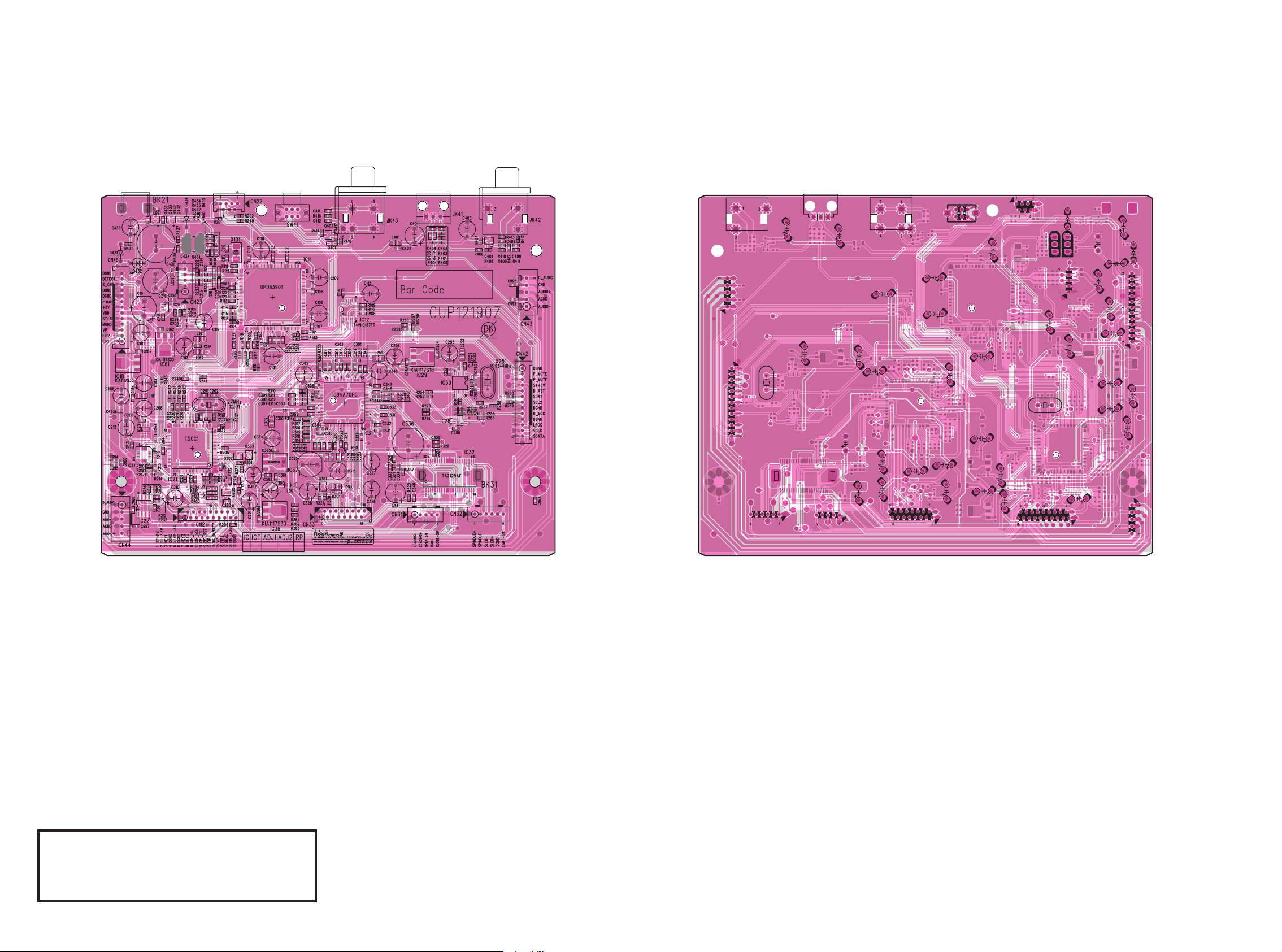
鉛フリー半田
半田付けには、鉛フリー半田 (Sn-Ag-Cu) を使用してください。
Lead-free Solder
When soldering, use the Lead-free Solder (Sn-Ag-Cu).
43 44
13. PARTS LOCATION
MAIN A PWB MAIN B PWB
Page 30

鉛フリー半田
半田付けには、鉛フリー半田 (Sn-Ag-Cu) を使用してください。
Lead-free Solder
When soldering, use the Lead-free Solder (Sn-Ag-Cu).
45 46
FRONT1 A PWB
FRONT 1 B PWB
Page 31

鉛フリー半田
半田付けには、鉛フリー半田 (Sn-Ag-Cu) を使用してください。
Lead-free Solder
When soldering, use the Lead-free Solder (Sn-Ag-Cu).
47 48
FRONT2 A PWB
FRONT3 A PWB
FRONT2 B PWB
FRONT3 B PWB
Page 32

鉛フリー半田
半田付けには、鉛フリー半田 (Sn-Ag-Cu) を使用してください。
Lead-free Solder
When soldering, use the Lead-free Solder (Sn-Ag-Cu).
49 50
POWER1 A PWB POWER1 B PWB
Page 33

鉛フリー半田
半田付けには、鉛フリー半田 (Sn-Ag-Cu) を使用してください。
Lead-free Solder
When soldering, use the Lead-free Solder (Sn-Ag-Cu).
51 52
POWER3 A PWB POWER3 B PWB
POWER2 A PWB POWER2 B PWB
Page 34

53 54
DESCRIPTION Q'TYNO. VERS. COLOR PARTS NO.
CTW3+12JR
S9
4
CTB3+10JR
S8
12
A/S PART
O.K
O.K
S7
S6 N1B
O.K
CTW3+8JFZR 6
S5
O.K
CTW3+8JR 6
S4
O.K
CTB3+8JFB 19
S3
O.K
CTBD3+8JFB 1
S2
O.K
CTB3+6FFB 2
S1
O.K
5
CTB3+6JR 16
CTB3+10JFB
O.K
CTW3+18JR 3
SCREW
S10
SCREW
SCREW
SCREW , DOT
SCREW
SCREW
S6 N1SG, FN
O.K
CTW3+8JFC 6SCREW
SCREW
SCREW
SCREW
SCREW
O.K
S11
CHD2A023R 4SCREW
O.K
40
41
42
S4
x1
S4
x1
S4
x2
S4
x3
S4
S4
S1
S1
x4
x2
x1
x1
S7
x8
S7
x2
S7
x2
S1
x1
S1
x1
S9
x2
S5
x1
S9
x2
S10
x3
S5
x1
S6
x3
S1
x4
x4
S1
S4
x1
S2
x2
S8
x3
S3
x1
S8
x2
S4
x1
1
2
3
4
5
6
7
8
9
10
15
11
11
12
14
17
18
16
19
13
13
20
21
23
49
22
24
24
25
26
27
28
31
30
29
32
33
S6
x3
34
35
36
36
36
36
36
36
37
38
44
S4
x2
S1
x4
S5
x4
39
41
42
50
43
S11
x2
S11
x2
45
S4
x2
46
F Only
N Only
K Only
14. EXPLODED VIEW AND PARTS LIST
Page 35

55 56
NOTE : "nsp" PART IS LISTED FOR REFERENCE ONLY, D&M WILL NOT SUPPLY THESE PARTS. NOTE : "nsp" PART IS LISTED FOR REFERENCE ONLY, D&M WILL NOT SUPPLY THESE PARTS.
POS.
NO.
VERS.
COLOR
PART NO.
(FOR EUR)
PART NO.
(MZ)
PART NAME DESCRIPTION
1 421410006004M 421410006004M BADGE MARANTZ BADGE (AL) M1 MODEL CGB1A206
18 nsp nsp BRACKET BRACKET HEADPHONE CMD1A677
44 FN nsp 943411007030M BUTTON BUTTON, USB CBT1A1109RMD10
44 K1SG nsp 943411007030M BUTTON BUTTON, USB CBT1A1109RMD10
44 N1SG 943411007030M 943411007030M BUTTON BUTTON, USB CBT1A1109RMD10
44 N1B 943411007040M 943411007040M BUTTON BUTTON, USB CBT1A1109
14,15,16 nsp nsp PCB CD6003CDFRONTPCBASS'Y COP12191B
9 481510003006M 481510003006M LENS LENS POWER INDICATOR CGL1A274
34 FN nsp 00M24AW154120 KNOB KNOB LEVEL SG CBN1A170RMD10
34 K1SG nsp 00M24AW154120 KNOB KNOB LEVEL SG CBN1A170RMD10
N1B 943411007050M 943411007050M KNOB KNOB, LEVEL CBN1A170B37
34 N1SG 00M24AW154120 00M24AW154120 KNOB KNOB LEVEL SG CBN1A170RMD10
11 FN nsp 411510019033M BUTTON BUTTON 3 KEY SG CBT1A1084RMD10
11 K1SG nsp 411510019033M BUTTON BUTTON 3 KEY SG CBT1A1084RMD10
11 N1B 411510019002M 411510019002M BUTTON BUTTON 3 KEY BL CBT1A1084
11 N1SG 411510019033M 411510019033M BUTTON BUTTON 3 KEY SG CBT1A1084RMD10
10 FN nsp 411510021036M BUTTON BUTTON POWER SWITCH SG CBT1A1072RMD10
10 K1SG nsp 411510021036M BUTTON BUTTON POWER SWITCH SG CBT1A1072RMD10
10 N1SG 411510021036M 411510021036M BUTTON BUTTON POWER SWITCH SG CBT1A1072RMD10
10 N1B 411510015017M 411510015017M BUTTON BUTTON POWER TACT BL CBT1A1072
2 FN nsp 943418002180M ESCUTCHEON ORNAMENT DOOR SG CGR1A455RMYD10
2 K1SG nsp 943418002180M ESCUTCHEON ORNAMENT DOOR SG CGR1A455RMYD10
2 N1B 943418002170M 943418002170M ESCUTCHEON ORNAMENT DOOR BL CGR1A455ZB37
2 N1SG 943418002180M 943418002180M ESCUTCHEON ORNAMENT DOOR SG CGR1A455RMYD10
4 FN nsp 943402007060M PANEL PANEL, ALFRONT CKM2A203XC62
4 K1SG nsp 943402007060M PANEL PANEL, ALFRONT CKM2A203XC62
4 N1B 943402007070M 943402007070M PANEL PANEL, ALFRONT CKM2A203WC23
4 N1SG 943402007060M 943402007060M PANEL PANEL, ALFRONT CKM2A203XC62
6 N1B 943402002130M 943402002130M PANEL L SIDE FRONT PANEL CD5003 BL CGW1A463RNZB37
6 FN nsp 943402002140M PANEL L SIDE FRONT PANEL CD5003 SG CGW1A463ROYD10
6 K1SG nsp 943402002140M PANEL L SIDE FRONT PANEL CD5003 SG CGW1A463ROYD10
6 N1SG 943402002140M 943402002140M PANEL L SIDE FRONT PANEL CD5003 SG CGW1A463ROYD10
7 N1B 943402007080M 943402007080M PANEL PANEL, SIDERCD5003/N1B CGW1A464RNB37
7 FN nsp 943402007090M PANEL PANEL, SIDERCD5003/N1SG CGW1A464ROD10
7 K1SG nsp 943402007090M PANEL PANEL, SIDERCD5003/N1SG CGW1A464ROD10
7 N1SG 943402007090M 943402007090M PANEL PANEL, SIDERCD5003/N1SG CGW1A464ROD10
5 FN nsp 443510004038M CHASSIS CHASSIS CENTER MOLD SG CGW1A462RMD10
5 K1SG nsp 443510004038M CHASSIS CHASSIS CENTER MOLD SG CGW1A462RMD10
5 N1SG 443510004038M 443510004038M CHASSIS CHASSIS CENTER MOLD SG CGW1A462RMD10
5 N1B 443510004007M 443510004007M CHASSIS CHASSIS CENTER MOLD BL CGW1A462B37
45 nsp nsp PLATE PLATE, EARTHUSB CMC1A370
8 nsp nsp SHEET SHEET LED CGX1A411Z
50 nsp nsp WASHER CNW2A028
3 943416007190M 943416007190M WINDOW WINDOW, FIP CGU1A423A12Y
FN nsp nsp CORD 5P WIRE ASSY 250MM CWB1B005250EG
K1SG nsp nsp CORD 5P WIRE ASSY 250MM CWB1B005250EG
N1SG nsp nsp CORD 5P WIRE ASSY 250MM CWB1B005250EG
FN nsp nsp CORD WIRE ASSY 9P 280MM CWZCD5003BN81
N1B nsp nsp CORD WIRE ASSY 9P 280MM CWZCD5003BN81
N1SG nsp nsp CORD WIRE ASSY 9P 280MM CWZCD5003BN81
nsp nsp LABEL A-ROHS/LABEL,SERIAL CQB1D022
943606007100M 943606007100M FPC
CABLE,CARD,CDMECHA(16P,150MM,1MM,BType)
CWC4F2A16A150B10
30 FN nsp nsp PCB CD6003CDMAINPCBASS'Y COP12190B
30 K1SG nsp nsp PCB CD6003CDMAINPCBASS'Y COP12190B
30 N1 nsp nsp PCB CD6003CDMAINPCBASS'Y COP12190B
28 943302002290M 943302002290M MECHANISM MECHA LOADER AND TRAVERSE CJDWSL11VF
943302007110M 943302007110M MECHANISM CDMECHANISMASS'Y(CD6003) CJDCD6003ZA
FN nsp nsp CLAMPER CLAMPER CHR301
K1SG nsp nsp CLAMPER CLAMPER CHR301
N1B nsp nsp CLAMPER CLAMPER CHR301
FN nsp nsp CLAMPER CHE36-3
K1SG nsp nsp CLAMPER CHE36-3
N1B nsp nsp CLAMPER CHE36-3
35 nsp nsp COVER COVER SCREW CMD1A495
46 943533007120M 943533007120M CUSHION CUSHION CHG1A236
23 00M32CW107010 00M32CW107010 SHEET CUSHION FOOT CHG1A360
38 nsp nsp BUFFER CUSHION RUBBER CHG1A157
90M-FC500030R 90M-FC500030R FERRITE CORE FERRITE RING 29X7.7X19 CLZ9W003Z
POS.
NO.
VERS.
COLOR
PART NO.
(FOR EUR)
PART NO.
(MZ)
PART NAME DESCRIPTION
22 00M243W057210 00M243W057210 LEG LEG FOR SILVER CKL2A042H46
24 nsp nsp HOLDER HOLDER PWB CHE170
25 nsp nsp HOLDER HOLDER,PCB CHE2A030
32 FN nsp nsp PANEL PANEL, REAR CKF3A390Y
32 K1SG nsp nsp PANEL PANEL, REAR CKF3A390X
32 N1B nsp nsp PANEL PANEL, REAR CKF3A390Z
32 N1SG nsp nsp PANEL PANEL, REAR CKF3A390Z
39 00MYJ04002640 00MYJ04002640 INLET ! R-301(21) AC INLET CJJ8A006ZW
49 nsp nsp BUFFER RUBBER CHG1A113
nsp nsp SCREW CTB3+10JR CTB3+10JR
S4 nsp nsp SCREW COPPER PLATING CTB3+8JFB
S6 FN nsp nsp SCREW 0 CTW3+8JFC
S6 K1SG nsp nsp SCREW 0 CTW3+8JFC
S6 N1SG nsp nsp SCREW 0 CTW3+8JFC
S6 N1B nsp nsp SCREW 0 CTW3+8JFZR
S11 nsp nsp SCREW 0 CHD2A023R
27 nsp nsp BRACKET SUPPORT MECHANISM CMD1A676
36 nsp nsp TAPE TAPE HEMELON CHS1A032
37 nsp nsp WASHER WASHER GROUND COPPER CNW1A035
FN nsp nsp CORD WIRE ASSY CWB5A906220EG
K1SG nsp nsp CORD WIRE ASSY CWB5A906220EG
N1B nsp nsp CORD WIRE ASSY CWB5A906220EG
943535006220S 943535006220S BAG POLYETHY BAG 650*600 KPB1A013Y CPB1A013Y
nsp nsp BATTERY BATTERY (SIZE AAA) 2PCS IN 1PACK CABR03PPB
943606007140M 943606007140M FPC FFCCABLE,CARD(19P,1.0MM,250MM,B,8MM)
CWC4F4A19A250B08
21 nsp nsp CHASSIS CHASSIS, BOTTOM CUA2A289
nsp 90M-FC500030R FERRITE CORE FERRITE RING 29X7.7X19 CLZ9W003Z
20 nsp nsp FRAME FRAME, FRONT CUF2A004
nsp nsp HEATSINK HEAT SINK CMY2A223
K1SG nsp nsp CABLE HEMELONTAPE(CABLE) CHS1A148
nsp 00MHC3650509F IC NJU7223F50 CVINJU7223F50
nsp nsp CORD WIRE ASSY
CWZCD6002BN95ZA
FN nsp nsp LABEL LABEL,WHITEM1SG CQB1A908Z
K1SG nsp nsp LABEL LABEL,WHITEM1SG CQB1A908Z
N1SG nsp nsp LABEL LABEL,WHITEM1SG CQB1A908Z
17 nsp nsp NUT NUT PHONE CNE1A013
43 nsp nsp PLATE PLATE,BOTTOM CUA1A298
00MHC3890599F 00MHC3890599F IC KIA7805API HVIKIA7805API
S8 nsp nsp SCREW CTB3+10JFB CTB3+10JFB
S7 K1SG nsp nsp SCREW CTB3+10JR CTB3+10JR
S2 nsp nsp SCREW CTB3+6FFB
S1 nsp nsp SCREW CTB3+6JR
nsp nsp SCREW COPPER PLATING CTB3+8JFB
nsp nsp SCREW CTB3+8JR
S9 nsp nsp SCREW CTW3+12JR
S10 nsp nsp SCREW CTW3+18JR CTW3+18JR
S5 nsp nsp SCREW CTW3+8JR
S3 nsp nsp SCREW CTBD3+8JFB
00MHT21020100 00MHT21020100 TRS. 2SB1020A CVT2SB1020A
00MHT41415100 00MHT41415100 TRS. 2SD1415A CVT2SD1415A
nsp nsp CORD WIRE ASSY CWZCD6002BN95
PACKING
FN nsp 943541007160M USER GUIDE USER GUIDE CD6003 F CQX1A1452Z
K1SG nsp 943541007170M USER GUIDE USER GUIDE CD6003 K CQX1A1454Z
N1 943541007180M 943541007180M USER GUIDE USER GUIDE CD6003 N CQX1A1453Z
307010035001M 307010035001M UNIT KIT REMOTE CONTROLLER RC002CD CARTCD5003M
42 K1SG nsp 90M-ZC000650R MAINS CORD ! MAINS CORD FOR K CJA2N075Z
41 N1 90M-ZC000320R 90M-ZC000320R MAINS CORD ! MAINS CORD 2WIRE 10A/250V CJA2B054Z
40 FN nsp 943611007150M MAINS CORD CORD,POWERJPNINLETTYPE CJA2J110ZV
NOT STANDARD SPARE PART
943531007130M 943531007130M CARTON BOX,OUTCARTON CPG1A870U
943533002300M 943533002300M CUSHION CUSHION CD5003 CPS1A821
33 N1B 401310003002M 401310003002M LID TOP COVER BL CKC2A187K117
33 FN nsp 401310003033M LID TOP COVER SG CKC2A187D11
33 K1SG nsp 401310003033M LID TOP COVER SG CKC2A187D11
33 N1SG 401310003033M 401310003033M LID TOP COVER SG CKC2A187D11
90M-ZD000440R 90M-ZD000440R CONN. CORD CORD PIN CJS4M009X
90M-ZD000510R 90M-ZD000510R CONN. CORD CORD PIN CJS4N014Z
Page 36

15. MICROPROCESSOR AND IC DATA
IC21 : T5CC1
Pin No Pin Port Name Use
1 VREFL GND - - - GMD for AD
2 AVSS GND - - - GND
3 AVCC ST+3.3V AVCC - - ST+3.3V
4 P70/TA0IN CD_LIMIT_SW I - - Limit SW of CD Loader
5 P71/TA1OUT CD_CLOSE_SW I - - Close SW of CD Loader
6 P72/TA3OUT CD_OPEN_SW I Open SW of CD Loader
7 P73/TA4IN CD_OPEN_M O H L Open Control for Motor Driver IC
8 P74/TA5OUT CD_CLOSE_M O H L Close Control for Motor Driver IC
9 P75/TA7OUT MT_STBY O L L Standby Control for Motor Driver IC
10 P80/TB0IN0/INT5 RS/REMOTE_IN Remote Input
11 P81/TB0IN1/INT6
12 P82/TB0OUT0
13 P83/TB0OUT1
14 P84/TB1IN0/INT7
15 P85/TB1IN1/INT8
16 P86/TB1OUT0 SDA2 O - - I2C Data for DAC/PLL
17 P87/TB1OUT1 SCL2 O - - I2C Clock for DAC/PLL
18 P90/TXD0 USB_SO UART - - Data Out for USB Control IC(uPD63901)
19 P91/RXD0 USB_SI UART - - Data In for USB Control IC(uPD63901)
20 P92/SCLK0/_CTS0 USB_CLK UART - - Clock for USB Control IC(uPD63901)
21 P93/TXD1 TXD UART - Data Out for RS-232
22 P94/RXD1 RXD UART - Data In from RS-232
23 P95/SCLK1/_CTS1
24 AM0 AM0 I - - Connect to DVCC
25 DVCC ST+3.3V DVCC - - ST+3.3V
26 X2 XOUT O - - 27MHz X'tal
27 DVSS GND - - - GND
28 X1 XIN I - - 27MHz X'tal
29 AM1 AM1 I - - Connect to DVCC
30 _RESET HOST_RESET I L H RESET
31 P96/XT1
32 P97/XT2
33 EMU0 EMU0 O - - OPEN
34 EMU1 EMU1 O - - OPEN
35 PA0/INT1 RS/REMOTE_IN I ↓ - Remote Input/Wake up Key Input
36 PA1/INT2 CD_REQ I ↑ - IREQ from CD DSP
37 PA2/INT3 USB_CTS I ↓ - CTS for USB Control IC(uPD63901)
38 PA3/INT4 PWR_D I ↑ - Power Down Detect
39 PA4 A_MUTE O H H Analog Mute
40 PA5 DAC_RST O L H DAC IC Reset
41 PA6 CD_USB O - L L:CD, H:USB
42 PA7
43 ALE - - - Disable
44 P00/AD0 CD_BUS0 O - H Data In/Out bus for CD DSP
45 P01/AD1 CD_BUS1 I/O - H Data In/Out bus for CD DSP
46 P02/AD2 CD_BUS2 I/O - H Data In/Out bus for CD DSP
47 P03/AD3 CD_BUS3 I/O - H Data In/Out bus for CD DSP
48 P04/AD4 CD_CCC I/O L H Chip Enable for CD DSP
49 P05/AD5 CD_BUCK O L H Clock Out for CD DSP
50 P06/AD6 CD_RST O L H Reset to CD DSP
51 P07/AD7
52 P10/AD8/A8 USB_STBY_B O L H
53 P11/AD9/A9 IPOD_ERR I - - iPod Error from USB Control IC(uPD63901)
PortSetup
Act. Init
Note
Standby Control for USB Control
IC(uPD63901)
57
Page 37

58
Pin No Pin Port Name Use
54 P12/AD10/A10 USB_DDI I - - USB Error From USB Control IC(uPD63901)
55 P13/AD11/A11 USB_RTS O L H RTS for USB Control IC(uPD63901)
56 P14/AD12/A12 USB_NMI I - 57 P15/AD13/A13 USB_RESET O L H Reset for USB Control IC(uPD63901)
58 P16/AD14/A14 STBY_CNT O L L Standby Control L : Standby, H : Normal
59 P17/AD15/A15 IPOD_RST O L H Reset for iPod CP Chip
60 P20/A0/A16 IPOD_SDA I/O - H I2C Data for iPod CP
61 P21/A1/A17 IPOD_SCL I/O - H I2C Clock for iPod CP
62 DVSS GND - - - GND
63 _NMI _NMI I - - ST+3.3V
64 DVCC ST+3.3V DVCC - - ST+3.3V
65 P22/A2/A18
66 P23/A3/A19
67 P24/A4/A20
68 P25/A5/A21
69 P26/A6/A22
70 P27/A7/A23
71 P30/_RD
72 P31/_WR
73 P32/_HWR
74 P33/_WAIT
75 P34/_BUSRQ
76 P35/_BUSAK
77 P36/R/_W
78 P37/_BOOT BOOT I - - Single Boot Mode (at P37=Low)
79 P40/_CS0 DIS_SO O - H Data Output for VFD
80 P41/_CS1 DIS_SCL O - H Clock Output for VFD
81 P42/_CS2 DIS_CS O L H CS for VFD
82 P43/_CS3 DIS_RESET O L H Reset for VFD
83 P60/SCK
84 P61/SO/SDA SDA I/O I2C Data for EEPROM
85 P62/SI/SCL SCL O I2C Clock for EEPROM
86 P63/INT0
87 P64/SCOUT STBY_LED O L L
88 P65 DIS_OFF_LED O H L Display Off LED On
89 DVCC ST+3.3V DVCC - - ST+3.3V
90 P66
91 DVSS GND - - - GND
92 P50/AN0 KEY0 AD - - Front Key In 0
93 P51/AN1 KEY1 AD - - Front Key In 1
94 P52/AN2 KEY2 AD - - Front Key In 2
95 P53/AN3/_ADTRG DETECT AD - - 2 times AC voltage input detect
96 P54/AN4 AD
97 P55/AN5 AD
98 P56/AN6 MODEL_SEL0 AD - - Model Select0
99 P57/AN7 MODEL_SEL1 AD - - Model Select1
100 VREFH ST+3.3V - - - ST+3.3V for AD
PortSetup
Act. Init
Note
Standby detect from USB Control
IC(uPD63901)
Standby LED Control Normal : L,
Standby : H -> Input Port
Page 38

59
IC27 : CDCE913PWR
1
FEATURES
APPLICATIONS
Xin/CLK
1 14
Xout
S0
2 13
S1/SDA
V
DD
3 12
S2/SCL
V
ctr
4 11
Y1
GND
5 10
GND
V
DDOUT
69
Y2
78
Y3
VCXO
XO
LVCMOS
LV
CMOS
LV
CMOS
PLL
with�SSC
LV
CMOS
Divider
and
Output
Control
3
EEPROM
Programming
and
Control�Register
V
ctr
Crystal�or
Clock�Input
S2/S1/S0�or
SDA/SCL
V
DD
GND
V
DDOUT
Y1
Y2
Y3
V
DDOUT
CDCE913
CDCEL913
SCAS849B–JUNE 2007–REVISED DECEMBER 2007
www.ti.com
Programmable 1-PLL VCXO Clock Synthesizer With 1.8-V, 2.5-V, and 3.3-V Outputs
• Flexible Clock Driver
2345
• Member of Programmable Clock Generator – Three User-Definable Control Inputs
Family [S0/S1/S2], for example., SSC Selection,
Frequency Switching, Output Enable, or
– CDCE913/CDCEL913: 1-PLL, 3 Outputs
Power Down
– CDCE925/CDCEL925: 2-PLL, 5 Outputs
– Generates Highly Accurate Clocks for
– CDCE937/CDCEL937: 3-PLL, 7 Outputs
Video, Audio, USB, IEEE1394, RFID,
– CDCE949/CDCEL949: 4-PLL, 9 Outputs
Bluetooth™, WLAN, Ethernet™, and GPS
• In-System Programmability and EEPROM
– Generates Common Clock Frequencies
– Serial Programmable Volatile Register
Used With TI-DaVinci™, OMAP™, DSPs
– Nonvolatile EEPROM to Store Customer
– Programmable SSC Modulation
Setting
– Enables 0-PPM Clock Generation
• Flexible Input Clocking Concept
• 1.8-V Device Power Supply
– External Crystal: 8 MHz to 32 MHz
• Wide Temperature Range –40° C to 85° C
– On-Chip VCXO: Pull Range ±150 ppm
• Packaged in TSSOP
– Single-Ended LVCMOS up to 160 MHz
• Development and Programming Kit for Easy
• Free Selectable Output Frequency up to
PLL Design and Programming (TI Pro-Clock™)
230 MHz
• Low-Noise PLL Core
• D-TV, STB, IP-STB, DVD-Player, DVD-Recorder,
– PLL Loop Filter Components Integrated
Printer
– Low Period Jitter (Typical 50 ps)
• Separate Output Supply Pins
– CDCE913: 3.3 V and 2.5 V
– CDCEL913: 1.8 V
www.ti.com
DESCRIPTION
CDCE913
CDCEL913
SCAS849B–JUNE 2007–REVISED DECEMBER 2007
These devices have limited built-in ESD protection. The leads should be shorted together or the device placed in conductive foam
during storage or handling to prevent electrostatic damage to the MOS gates.
The CDCE913 and CDCEL913 are modular PLL-based low-cost, high-performance, programmable clock
synthesizers, multipliers, and dividers. They generate up to 3 output clocks from a single input frequency. Each
output can be programmed in-system for any clock frequency up to 230 MHz, using the integrated configurable
PLL.
The CDCx913 has separate output supply pins, V
DDOUT
, which is 1.8 V for CDCEL913 and 2.5 V to 3.3 V for
CDCE913.
The input accepts an external crystal or LVCMOS clock signal. If an external crystal is used, an on-chip load
capacitor is adequate for most applications. The value of the load capacitor is programmable from 0 to 20 pF.
Additionally, an on-chip VCXO is selectable which allows synchronization of the output frequency to an external
control signal, that is, PWM signal.
The deep M/N divider ratio allows the generation of zero-ppm audio/video, networking (WLAN, BlueTooth,
Ethernet, GPS) or interface (USB, IEEE1394, Memory Stick) clocks from e.g., a 27 MHz reference input
frequency.
The PLL supports SSC (spread-spectrum clocking). SSC can be center-spread or down-spread clocking which is
a common technique to reduce electro-magnetic interference (EMI).
Based on the PLL frequency and the divider settings, the internal loop filter components are automatically
adjusted to achieve high stability and optimized jitter transfer characteristic.
The device supports non-volatile EEPROM programming for ease customization of the device to the application.
It is preset to a factory default configuration (see the DEFAULT DEVICE CONFIGURATION section). It can be
re-programmed to a different application configuration before PCB assembly, or re-programmed by in-system
programming. All device settings are programmable through SDA/SCL bus, a 2-wire serial interface.
Three programmable control inputs, S0, S1 and S2, can be used to select different frequencies, or change SSC
setting for lowering EMI, or other control features like, outputs disable to low, outputs 3-state, power down, PLL
bypass etc).
The CDCx913 operates in a 1.8 V environment. It operates in a temperature range of –40° C to 85° C.
Terminal Functions for CDCE913, CDCEL913
TERMINAL
I/O DESCRIPTION
NAME PIN TSSOP14
Y1–Y3 11, 9, 8 O LVCMOS outputs
Xin/CLK 1 I Crystal oscillator input or LVCMOS clock Input (selectable via SDA/SCL bus)
Xout 14 O Crystal oscillator output (leave open or pullup when not used)
V
Ctrl
4 I VCXO control voltage (leave open or pullup when not used)
V
DD
3 Power 1.8-V power supply for the device
CDCEL913: 1.8-V supply for all outputs
V
DDOUT
6, 7 Power
CDCE913: 3.3-V or 2.5-V supply for all outputs
GND 5, 10 Ground Ground
S0 2 I User-programmable control input S0; LVCMOS inputs; internal pullup 500k
SDA: bidirectional serial data input/output (default configuration), LVCMOS internal
SDA/S1 13 I/O or I pullup; or
S1: user-programmable control input; LVCMOS inputs; internal pullup 500k
SCL: serial clock input LVCMOS (default configuration), internal pullup 500k or
SCL/S2 12 I
S2: user-programmable control input; LVCMOS inputs; internal pullup 500k
Page 39

60
IC31 : TC94A70FG
Description
TC94A70FG and TC94A73MFG are highly
integrated, high-performance CD-MP3
solutions that enable playback of CD and
multiple compressed audio formats from a
single chip. Featuring high-quality audio
output in I
2
S, S/PDIF or analog stereo
formats, the TC94A70FG integrates an RF
amplifier, CD servo, audio DSP, 1 Mbit
SRAM, and a multi-bit DA converter in a
CMOS monolithic IC. To the TC94A70FG
feature set, the TC94A73MFG adds
electronic shock protection (ESP) with
DSP firmware and 16 Mbit DRAM in an
SiP solution. TC94A70FG and
TC94A73MFG are available in standard
ROM versions or can also be customized
to specific customer requirements using
an extensive and growing DSP firmware
library including MP3, WMA, ATRAC CD,
AAC, graphic equalization and popular
surround sound formats. Pin compatibility
between the monolithic TC94A70FG and
the SiP TC94A73MFG minimizes the
TC94A70FG/TC94A73MFG
Single-chip CD-MP3 Processor
engineering investment needed to upgrade
TC94A70FG CD playback designs with ESP.
New product design is further aided by
programmable RAM and macro commands
that simplify CD mechanism playback and
compressed audio tag and file management.
High integration, software customization, and
pin-compatible packages make TC94A70FG
and TC94A73MFG ideal for compressed
audio CD players where low cost, feature
flexibility and time to market are key
selection criteria.
Supported Product Families
• TC94A70FG-002:
MP3, WMA9 and ATRAC CD DSP
firmware
• TC94A70FG-005:
MP3, WMA9, ATRAC CD and AAC DSP
firmware
• TC94A73MFG-201:
MP3, WMA9 and ESP DSP firmware
• TC94A73MFG-202:
MP3, WMA9, ATRAC CD, AAC and ESP
DSP firmware
CD–RF
IN
CD–RF
Amp
Audio
DAC
Analog
Post
Filter
Servo
ADC
CDP
DSP
24-Bit
DSP
1 Mbit
SRAM
Servo
Processor
Servo
DAC
Peripheral
I/F
PLL/VCO
16 Mbit
DRAM
Audio
Out
3.3V 1.5V
SiP
TC94A73MFG
Only
Block Diagram
TC94A70FG
Pin description (top view)
LPFN
TMAX
TMAXS
PDo
PVDD3
AWRC
VSS
VDD1
LRCKi(Pi6)
BCKi(Pi5)
AiN(Pi4)
LRCK(Po9)
BCK(Po8)
AoUT1(Po7)
DoUT(Po6)
MS
GPIN
ZDET
SFSY
IPF
SBOK
SBSY
VDDT3
VSS
Pio3
75747372717069686766656463626160595857565554535251
LPFo
76 50
Pio2
PVREF
77 49
Pio1
VCoF
78 48
Pio0
PVSS3
79 47
AoUT2(Po5)
SLCo
80 46
AoUT3(Po4)
RFi
81 45
IRQ
RFRPi
82 44
TEST
RFEQo
83 43
/CCE
VRo
84 42
BUCK(CLK)
RESiN
85 41
BUS3(Si)
VMDiR
86 40
BUS2(So)
TESTR
87 39
BUS1
AGCi
88 38
BUS0
RFo
89 37
/RST
RVDD3
90 36
SRA
MSTB
LDo
91 35
VD
DM1
MDi
92 34
VDD1
RVSS3
93 33
VSS
FNi2
94 32
VDDT3
FNi1
95 31
DVSS3
FPi2
96 30
Lo
FPi1
97 29
DVR
TPi
98 28
DVDD3
TNPC
99 27
Ro
TNi
100 26
DVSS3
123456789
101112131415161718192021222324
25
AVSS3
RFZi
RFRP
SBAD/RFDC
FEi
TEi
TEZi
AVDD3
Foo
TRo
VREF
FMo
DMo
VSSP3
VCOi
VDDP3
VDD1
VSS
FGiN
io0(/HSo)
io1(/UHSo)
XVSS3
Xi
Xo
XVDD3
Zipang
1chip CDMP3
T
C94A70FG
TC94A70FG
1. Pin Descriptions
Pin
No.
Symbol I/O Description Default Remarks
1
AVSS3
-
Grounding pin for 3.3V CD analog circuits.
-
2
RFZi
I
3AI/F
Input pin for RF ripple zero-cross signal. I
Connect to RFRP by
0.033uF
3
RFRP
O
3AI/F
RF ripple signal output pin. O
4
SBAD/RFDC
O
3AI/F
Sub beam addition signal or
RFDC (Hologram PUH RF peak detection
signal) signal output pin
O
5
FEi
O
3AI/F
Focus error signal input pin. O
6
TEi
O
3AI/F
Tracking error signal input pin. O
Monitor pin for the signal.
7
TEZi
I
3AI/F
Tracking error signal zero-cross input pin. I Connect to TEI by 0.033uF
8
AVDD3
-
Power supply pin for 3.3 V CD analog
circuits.
-
9
Foo
O
3AI/F
Focus servo equalizer output pin. O
10
TRo
O
3AI/F
Tracking servo equalizer output pin.
O
Built-in series resister 3.3k
Ω
11
VREF
-
Reference voltage pin for analog
circuits(1.65V)
-
Connect to VRO and
PVREF. Connect 0.1uF
12
FMo
O
3AI/F
Feed servo equalizer output pin. O
13
DMo
O
3AI/F
Disc servo equalizer output pin O
Built-in series resister
3.3kΩ 3-state output
(AVDD3,AVSS3,VREF)
14
VSSP3
-
Grounding pin for 3.3V DSP VCO circuits.
-
15
VCOi
I
3AI/F
DSP VCO control voltage inputr pin.
I
16
VDDP3
-
Power supply pin for 3.3V DSP VCO
circuit.
-
17
VDD1
-
Power supply pin for 1.5V digital circuit
-
18
VSS
-
Grounding pin for 1.5V digital circuit.
-
19
FGiN
I
3I/F
FG signal input pin for CAV.
CLV: "L", CAV: FG input
I Analog input
20
io0(/HSo)
I/O
3I/F
General Input/output port -0 (CD)
(Playback speed mode flag output pin.)
I
Schmitt input
CMOS PORT
21
io1(/UHSo)
I/O
3I/F
General Input/output port -1 (CD)
(Playback speed mode flag output pin.)
I
Schmitt input
CMOS PORT
22
XVSS3
-
Grounding pin for 3.3V system clock
oscillator circuit.
-
23
Xi
I
3AI/F
Input pin for system clock oscillator
Circuit (External Rfb=1M:)
I X'tal
24
Xo
O
3AI/F
Output pin for system clock oscillator
circuit
O X'tal
25
XVDD3 -
Power supply pin for 3.3 V system clock
oscillator circuit
-
TC94A70FG
Pin
No.
Symbol I/O Description
Default Remarks
26
DVSS3
-
Grounding pin for 3.3V DAC circuit
-
27
Ro
O
3AI/F
R channel audio output pin of Audio DAC. O
28
DVDD3
-
Power supply pin for 3.3V Audio DAC
circuit.
-
29
DVR
-
Reference voltage pin for Audio DAC.
-
30
Lo
O
3AI/F
L channel audio output pin of Audio DAC O
31
DVSS3
-
Grounding pin for 3.3V Audio DAC circuit
-
No capacitor required to
DVR pin when built-in
audio DAC is not in use,
however , connect 3.3V to
DVDD3 and GND to
DVSS3.
32
VDDT3
-
Power supply pin for 3.3 V digital I/O circuit.
-
For CD and DSP I/O
33
VSS
-
Grounding pin for 3.3V digital circuit
-
-
34
VDD1
-
Power supply pin for 1.5V digital circuit.
-
-
35
VDDM1
-
Power supply pin for 1.5V 1Mbit SRAM.
-
36
SRAMSTB
I
3I/F
1Mbit SRAM stand-by pin I Schmitt input
37
/RST
I
3I/F
Reset signal input pin. I Schmitt input
38
BUS0
IO
3I/F
Data input/output pin -0 for
microcontroller interface
I
Schmitt input
CMOS PORT
39
BUS1
IO
3I/F
Data input/output pin -1 for
microcontroller interface
I
Schmitt input
CMOS PORT
40
BUS2(So)
IO
3I/F
Data input/output pin -2 for
microcontroller interface (Serial output)
I
Schmitt input
CMOS PORT
41
BUS3(Si)
IO
3I/F
Data input/output pin -3 for
microcontroller interface (Serial input)
I
Schmitt input
CMOS PORT
42
BUCK(CLK)
I
3I/F
Clock input pin for the microcontroller
interface. (Clock input for Serial
communication interface)
I Schmitt input
43
/CCE
I
3I/F
Chip enable signal input pin for
microcontroller interface.
I Schmitt input
44
TEST
I
3I/F
Setting pin for LSI test mode.
(Connect to GND in normal operation)
I Schmitt input
45
IRQ
I
3I/F
DSP interruption pin.(Pull down by 100k:
when not in use)
I Schmitt input
46
AoUT3(Po4)
O
3I/F
Audio data output pin -3 (DSP general
output port -4)
O CMOS PORT
47
AoUT2(Po5)
O
3I/F
Audio data output pin -2 (DSP general
output port -5)
O CMOS PORT
48
Pio0
I/O
3I/F
DSP general input/output port -0 I
Schmitt input
CMOS PORT
49
Pio1
I/O
3I/F
DSP general input/output port -1 I
Schmitt input
CMOS PORT
50
Pio2
I/O
3I/F
DSP general input/output port -2 I
Schmitt input
CMOS PORT
51
Pio3
I/O
3I/F
DSP general input/output port -3
I
Schmitt input
CMOS PORT
52
VSS
-
Grounding pin for 3.3V digital circuit
-
-
53
VDDT3
-
Power supply pin for 3.3 V digital I/O circuit.
-
For CD and DSP I/O
54
SBSY
O
3I/F
Sub code block sync output pin O CMOS PORT
55
SBOK
O
3I/F
CRCC check result output pin for sub code
Q data.
O CMOS PORT
Page 40

61
IC31 : TC94A70FG
TC94A70FG
Pin
No.
Symbol I/O Description Default Remarks
56
IPF
O
3I/F
Correction flag output O CMOS PORT
57
SFSY
O
3I/F
Servo internal register read clock output pin O CMOS PORT
58
ZDET
O
3I/F
Internal Audio DAC Zero data detection flag
output
O CMOS PORT
59
GPIN
I
3I/F
CD General Input port(Pull down by 100K:
when not in use)
I Schmitt input
60
MS
I
3I/F
Microprocessor I/F mode selection pin.
“L”: Parallel I/F, “H”: Serial I/F
I
61
DoUT(Po6)
O
3I/F
Digital Audio output (SPDIF) pin
(DSP general output port -6)
O CMOS PORT
62
AoUT1(Po7)
O
3I/F
Audio data output pin -1(DSP general
output port -7)
O CMOS PORT
63
BCKo(Po8)
O
3I/F
Bit clock output pin for AoUT
(DSP general output port -8)
O CMOS PORT
64
LRCKo(Po9)
O
3I/F
L/R channel clock output pin
(DSP general output port -9)
O CMOS PORT
65
AiN(Pi4)
I
3I/F
Audio data input for Audio DAC
(DSP general input port -4)
I Schmitt input
66
BCKi(Pi5)
I
3I/F
Bit clock input pin for AiN
(DSP general input port -5)
I Schmitt input
67
LRCKi(Pi6)
I
3I/F
L/R channel clock for AiN
(DSP general input port -6)
I Schmitt input
68
VDD1
-
Power supply pin for 1.5V digital circuit.
-
69
VSS
-
Grounding pin for 1.5V digital circuit.
-
70
AWRC
O
3AI/F
VCO control pin for active wide-range PLL O
Applicable in CLV/CAV
mode. Connect 0.033 uF.
71
PVDD3
-
Power supply pin for 3.3V CD PLL circuit.
-
72
PDo
O
3AI/F
EFM and PLCK Phase difference signal
output pin.
O
4-state output (
PVDD3,
Hiz,PVSS3,PVREF)
73
TMAXS
O
3AI/F
TMAX detection result output pin O
3-state output
(PVDD3,PVSS3,HiZ)
74
TMAX
O
3AI/F
TMAX detection result output pin O
3-state
output(PVDD3,PVSS3,HiZ)
75
LPFN
I
3AI/F
PLL circuit LPF amplifier inversion input pin I
Connect resister of LPF,
refer to application circuit
diagram.
76
LPFo
O
3AI/F
PLL circuit LPF amplifier Output pin O
Connect capacitor of LPF,
refer to application circuit
diagram.
77
PVREF
-
PLL circuit 1.65 V reference voltage pin.
-
Connected to VREF and
VRO inside of IC. Connect
0.1uF.
78
VCoF
O
3AI/F
VCO filter pin O Connect 0.01uF.
79
PVSS3
-
Grounding pin for 3.3V CD PLL circuit.
-
80
SLCo
O
3AI/F
EFM slice level output pin.
Output impedance =2.5kΩ both of
analog/digital slice mode.
O
Connect capacitor
according with servo
frequency band.
81
RFi
I
3AI/F
RF signal input pin
Zin is selectable by command.
I
Zin:20kΩ,10kΩ,5kΩ
82
RFRPi
I
3AI/F
RF ripple signal input pin I
TC94A70FG
Pin
No.
Symbol I/O Description Default Remarks
83
RFEQo
O
3AI/F
RF equalizer circuit output pin. O
Connect to RFRPI by
0.1uF, to RFI by 4700pF.
84
VRo
O
3AI/F
1.65 V reference voltage output pin. O
Connected to VREF and
PVREF inside of IC.
Connect 0.1uF+100uF.
85
RESiN
O
3AI/F
Pin for connecting a resistor for reference
current generation.
O
Connect 22kΩ//0.01uF.
86
VMDiR
-
Reference voltage output pin for LD APC.
-
Connect 0.1uF
87
TESTR
O
3AI/F
LPF connection pin for RFEQO offset
correction circuit.
O
Connect more than
0.015uF.
88
AGCi
I
3AI/F
RF signal AGC amplifier input pin I
89
RFo
O
3AI/F
RF signal generation amplifier output pin O
90
RVDD3
-
Power supply for 3.3V RF amplifier core
circuit.
-
91
LDo
O
3AI/F
Laser diode amplifier output pin.
92
MDi
I
3AI/F
Monitor photodiode amplifier input pin. I
Reference
Voltage=178mVtyp.
93
RVSS3
-
Grounding pin for RF amplifier core circuit
-
94
FNi2
I
3AI/F
Main beam signal input pin.
To be connected to PIN diode C.
I
95
FNi1
I
3AI/F
Main beam signal input pin.
To be connected to PIN diode A.
I
96
FPi2
I
3AI/F
Main beam signal input pin.
To be connected to PIN diode D.
I
97
FPi1
I
3AI/F
Main beam signal input pin.
To be connected to PIN diode B.
I
98
TPi
I
3AI/F
Sub beam signal input pin.
To be connected to PIN diode F.
I
99
TNPC
O
3AI/F
TNI/TPI input common capacitor connection
pin.
O
Connect to VRO by
capacitor.
100
TNi
I
3AI/F
Sub beam signal input pin.
To be connected to PIN diode E.
I
* 3A I/F : : 3 V analog circuit input/output pin.
1.5 I/F : 1.5Vdigital input/output pin.
3 I/F : 3 V digital input/output pin.
Note: The servo output pins (FOO, TRO, FMO, and DMO) become undefined or GND level under the following
conditions:
x /RST pin Low
x Crystal oscillation stopped according to the instructions by the Stop crystal oscillation command
x Power supply for CD is OFF.
xSRAMSTB pin = High
To prevent the undefined pin states from affecting the servo circuitry or any other mechanical blocks in the
system, appropriate measures should be taken, such as using a driver IC supporting a standby feature to
place the system in standby mode while either of the above conditions is satisfied.
Page 41

62
IC32 : TA2125AF
TA2125AF
TA2125AF
out
= 5.1 Vp-p (VCC = 8 V, RL = 8 ƺ)
CE (H)
+ V
CE (L)
= 1.3 V (VR = VM = 8 V,
= 200 mA)
CC
= 5.0-9.0 V
Weight: g (typ.)
y
24
6 7 12 131 2
RL5
36
V
R
35 34 33 32 31 30
Control
Logic
3
STBY
STBY
RIN FIN
4ch
Driver
STB
IN3 IN4
REG
STB
29 2728
FIN
V
CC
26 25
REG OUT
N.C.
23 22 21
3 3 3 3
20 19
4
VCIN IN1
5
N.C. N.C.
3 3 3 3
15 16 17 18
IN2
N.C. N.C.
11 148 9
FIN
10
GND
Iref TSD
RL4 RL3
RL2 RL1
TA2125AF
No. Symbol Function
1 OUT5A Output terminal H-bridge
2 VM Supply voltage terminal for Logic H-bridge
3 OUT5B Output terminal H-bridge
4 V
CIN
Input reference voltage 4ch BTL
5 IN1 Input for ch1 4ch BTL
6 N.C. Open
7 N.C. Open
8 N.C. 8, 9, 10, 27, 28, 29 are connected to PW GND (FIN)
9 N.C. 8, 9, 10, 27, 28, 29 are connected to PW GND (FIN)
10 N.C. 8, 9, 10, 27, 28, 29 are connected to PW GND (FIN)
11 IN2 Input for ch2 4ch BTL
12 N.C. Open
13 N.C. Open
14 V
CC1
Supply voltage terminal for ch1/ch2 4ch BTL
15 OUT2M Inverted output for ch2 4ch BTL
16 OUT2P Non-inverted output for ch2 4ch BTL
17 OUT1M Inverted output for ch1 4ch BTL
18 OUT1P Non-inverted output for ch1 4ch BTL
19 OUT3P Non-inverted output for ch3 4ch BTL
20 OUT3M Inverted output for ch3 4ch BTL
21 OUT4P Non-inverted output for ch4 4ch BTL
22 OUT4M Inverted output for ch4 4ch BTL
23 V
CC2
Supply voltage terminal for ch3/ch4 4ch BTL
24 N.C. Open
25 REG Connection with BASE of PNP Tr Regulator
26 REG OUT Output for regulator (5 V) Regulator
27 N.C. 8, 9, 10, 27, 28, 29 are connected to PW GND (FIN)
28 N.C. 8, 9, 10, 27, 28, 29 are connected to PW GND (FIN)
29 N.C. 8, 9, 10, 27, 28, 29 are connected to PW GND (FIN)
30 REG STBY Standby control for regulator Regulator
31 IN4 Input for ch4 4ch BTL
32 IN3 Input for ch3 4ch BTL
33 STBY Standby control for 4ch BTL 4ch BTL
34 FIN Logic control input H-bridge
35 RIN Logic control input H-bridge
36 VR Supply voltage terminal for motor driver H-bridge
Page 42

63
120 dB, 192 kHz Multi-Bit DAC with Volume Control
Features
Advanced Multi-bit Delta-Sigma Architecture
– 120 dB Dynamic Range
– -107 dB THD+N
– Low Clock Jitter Sensitivity
– Differential Analog Outputs
PCM input
– 102 dB of Stopband Attenuation
– Supports Sample Rates up to 192 kHz
– Accepts up to 24 bit Audio Data
– Supports All Industry Standard Audio
Interface Formats
– Selectable Digital Filter Response
– Volume Control with 1/2 dB Step Size and
Soft Ramp
– Flexible Channel Routing and Mixing
– Selectable De-Emphasis
Supports Stand-Alone or I²C/SPI¥
Configuration
Embedded Level Translators
– 1.8 V to 5 V Serial Audio Input
– 1.8 V to 5 V Control Data Input
Direct Stream Digital (DSD)
– Dedicated DSD Input Pins
– On-Chip 50 kHz Filter to Meet Scarlet Book
SACD Recommendations
– Matched PCM and DSD Analog Output
Levels
– Non-Decimating Volume Control with
1/2 dB Step Size and Soft Ramp
– DSD Mute Detection
– Supports Phase-Modulated Inputs
– Optional Direct DSD Path to On-Chip
Switched Capacitor Filter
Control Output for External Muting
– Independent Left and Right Mute Controls
– Supports Auto Detection of Mute Output
Polarity
Typical Applications
– DVD Players
– SACD Players
– A/V Receivers
– Professional Audio Products
PCM
Serial
Interfa c e
Multibit
Modulator
Interpolation
Filter with
Volume Control
Internal Voltage
Reference
External
Mute
Control
Switched
Capacitor
DAC and
Filter
DSD
Interface
PCM Input
Left and Right
Mute Controls
Right
Differential
Output
Left
Differential
Output
DSD Input
DSD Processor
1.8 V to 5V
1.8 V to 5 V
-Volume control
-50kHz filter
Switched
Capacitor
DAC and
Filter
MUX
Direct DSD
Level Translator
Level
Translator
Hardware or I2C/SPI
Control Data
MUX
Multibit
Modulator
Interpolation
Filter with
Volume Control
MUX
MUX
3.3 V to 5 V 5 V
Register/Hardware
Configuration
CS4398
QD01 : CS4398
IC75 : CS4398
Page 43

IC75 : CS4398
CS4398
DSD_B DSD_A
DSD_SCLK VLS
SDIN VQ
SCLK AMUTEC
LRCK AOUTAMCLK AOUTA+
VD VA
DGND AGND
M3 (AD1/CDIN) AOUTB+
M2 (SCL/CCLK) AOUTB-
M1 (SDA/CDOUT) BMUTEC
M0 (AD0/CS) VREF
RST REF_GND
VLC FILT+
1
2
3
4
5
6
7
8 21
22
23
24
25
26
27
28
9
10
11
12 17
18
19
20
13
14 15
16
CS4398
Pin Name Pin # Pin Description
DSD_A
DSD_B
28
1
Direct Stream Digital Input (Input) - Input for Direct Stream Digital serial audio data.
DSD_SCLK 2 DSD Serial Clock (Input) - Serial clock for the Direct Stream Digital audio interface.
SDIN 3 Serial Audio Data Input (Input) - Input for two’s complement serial audio data.
SCLK 4 Serial Clock (Input) - Serial clock for the serial audio interface.
LRCK 5
Left Right Clock (Input) - Determines which channel, Left or Right, is currently active on
the serial audio data line.
MCLK 6 Master Clock (Input) - Clock source for the delta-sigma modulator and digital filters.
VD 7 Digital Power (Input) - Positive power for the digital section.
DGND 8 Digital Ground (Input) - Ground reference for the digital section.
RST 13 Reset
(Input) - The device enters system reset when enabled.
VLC 14 Control Port Power (Input) - Positive power for Control Port I/O.
FILT+ 15
Positive Voltage Reference (Output) - Positive reference voltage for the internal sam-
pling circuits.
REF_GND 16 Reference Ground (Input) - Ground reference for the internal sampling circuits.
VREF 17 Voltage Reference (Input) - Positive voltage reference for the internal sampling circuits.
BMUTEC
AMUTEC
18
25
Mute Control (Output) - The Mute Control pin is active during power-up initialization, mut-
ing, power-down or if the master clock to left/right clock frequency ratio is incorrect. During
reset, these outputs are set to a high impedance.
AOUTB+
AOUTB-
2019Differential Right Channel Analog Output (Output) - The full-scale differential analog
output level is specified in the Analog Characteristics specification table.
AGND 21 Analog Ground (Input) - Ground reference for the analog section.
VA 22 Analog Power (Input) - Positive power for the analog section.
AOUTA+
AOUTA-
2324Differential Left Channel Analog Output (Output) - The full-scale differential analog out-
put level is specified in the Analog Characteristics specification table.
VQ 26 Quiescent Voltage (Output) - Filter connection for internal quiescent voltage.
VLS 27 Serial Audio Interface Power (Input) - Positive power for serial audio interface I/O.
Stand-Alone Mode Definitions
M3
M2
M1
M0
9
10
11
12
Mode Selection (Input) - Determines the operational mode of the device.
Control Port Mode Definitions
AD1/CDIN 9
Address Bit 1 (I²C) / Control Data Input (SPI) (Input) - AD1 is a chip address pin in I²C
mode; CDIN is the input data line for the Control Port interface in SPI mode.
SCL/CCLK 10 Serial Control Port Clock (Input) - Serial clock for the serial Control Port.
SDA/CDOUT 11
Serial Control Data (I²C) / Control Data Output (SPI) (Input/Output) - SDA is a data I/O
line in I²C mode. CDOUT is the output data line for the Control Port interface in SPI mode.
AD0/CS
12
Address Bit 0 (I²C) / Control Port Chip Select (SPI) (Input) - AD0 is a chip address pin
in I²C mode; CS
is the chip select signal for SPI format.
QD01 : CS4398
64
Page 44

16. ELECTRICAL PARTS LIST
PARTS INFORMATION
RESISTORS
1) 00MGD05
2) 00MGD05
Examples ;
0.1Ω ....001 10Ω ....100 1kΩ ....102 100kΩ ....104
0.5Ω ....005 18Ω ....180 2.7kΩ ....272 680kΩ ....684
1Ω ....010 100Ω ....101 10kΩ ....103 1MΩ ....105
6.8Ω ....068 390Ω ....391 22kΩ ....223 4.7MΩ ....475
Note : Please distinguish 1/4W from 1/6W by the shape of parts
CAPACITORS
CERAMIC CAP.
3) 00MDD1 × × × × 370, Ceramic capacitor
Examples ;
±0.25pF ......0
±0.5pF ......1
±5% ......5
Tolerance of COMMON PARTS handled here are as follows :
0.5pF~ 5pF .... ±0.25pF
6pF~ 10pF ....±0.5pF
12pF~ 560pF ....±5%
0.5pF ....005 3pF ....030 100pF .... 101
1pF .... 010 10pF ....100 220pF .... 221
1.5pF ....015 47pF ....470 560pF .... 561
× × ×
140, Carbon lm xed resistor, ±5% 1/4W
× × ×
160, Carbon lm xed resistor, ±5% 1/6W
}
Resistance value
used actually.
Resistance value
}
Disc type
Temp.coeff.P350~N1000, 50V
Tolerance (Capacity deviation)
Capacity value
Capacity value
Tolerance
NOTE ON SAFETY FOR FUSIBLE RESISTOR :
The suppliers and their type numbers of fusible resistors
are as follows;
1. KOA Corporation
Part No. (MJI) Type No. (KOA) Description
00MNH05 × × × 140 RF25S × × × ×
00MNH05 × × × 120 RF50S × × × ×
00MNH85 × × × 110 RF73B2A × × × ×
00MNH95 × × × 140 RF73B2E × × × ×
2. Matsushita Electronic Components Co., Ltd
Part No. (MJI) Type No. (MEC) Description
00MNF05 × × × 140 ERD-2FCJ × ×
00MRF05 × × × 140
00MNF02 × × × 140
00MRF02 × × × 140
Examples ;
0.1Ω ....001 10Ω ....100 1kΩ ....102 100kΩ ....104
0.5Ω ....005 18Ω ....180 2.7kΩ ....272 680kΩ ....684
1Ω ....010 100Ω ....101 10kΩ ....103 1MΩ ....105
6.8Ω ....068 390Ω ....391 22kΩ ....223 4.7MΩ ....475
}
}
Resistance value
*
▲▲
▲ ▲
Resistance value
▲ ▲
ERD-2FCG
Resistance value
Ω
J (±5% 1/4W)
Ω
J (±5% 1/2W)
Ω
J (±5% 1/10W)
Ω
J (±5% 1/4W)
}
Resistance value
(0.1 − 10kΩ)
×
(±5% 1/4W)
×
× ×
(±2% 1/4W)
}
Resistance value
ABBREVIATION AND MARKS
CERAMIC CAP.
4) 00MDK16
Examples ;
100pF ....101 1000pF .... 102 10000pF ....103
470pF ....471 2200pF .... 222
ELECTROLY CAP. ( )
5) 00MEA
Examples ;
0.1µF ....104 4.7µF ....475 100µF ... 107
0.33µF ....334 10µF ....106 330µF ... 337
1µF ....105 22µF ....226 1100µF ... 118
2200µF ... 228
6.3V ....006 25V ....025
10V ....010 35V ....035
16V ....016 50V ....050
FILM CAP. ( )
6) 00MDF15
00MDF15
00MDF16
Examples ;
0.001µF (1000pF) .........102 0.1µF ....104
0.0018µF ........................182 0.56µF ....564
0.01µF ........................103 1µF ....105
0.015µF ........................153
× × ×
300, High dielectric constant ceramic
}
capacitor
Disc type
Temp.chara. 2B4, 50V
Capacity value
× × × × ×
}
One-way lead type, Tolerance ±20%
Capacity value
Working voltage
× × ×
× × ×
× × ×
}
One-way type, Mylar ±10% 50V
Capacity value
Capacity value
10, Electrolytic capacitor
×
}
Working voltage
Capacity value
350 Plastic lm capacitor
310 One-way type, Mylar ±5% 50V
310 Plastic lm capacitor
▲
▲
Capacity value
ANT. : ANTENNA BATT. : BATTERY
CAP. : CAPACITOR CER. : CERAMIC
CONN. : CONNECTING DIG. : DIGITAL
HP : HEADPHONE MIC. : MICROPHONE
µ-PRO : MICROPROCESSOR REC. : RECORDING
RES. : RESISTOR SPK : SPEAKER
SW : SWITCH
TRIM. : TRIMMING TRS. : TRAMSISTOR
VAR. : VARIABLE X’TAL : CRYSTAL
TRANSF.
: TRANSFORMER
NOTE ON FUSE :
Regarding to all parts of parts code 00MFS20xxx2xx, replace
only with Wickmann-Werke GmbH, Type 372 non glass type fuse.
NOTE ON SAFETY :
Symbol Fire or electrical shock hazard. Only original parts
should be used to replaced any part marked with symbol .
Any other component substitution (other than original type), may
increase risk of re or electrical shock hazard.
安全上の注意 :
がついている部品は、安全上重要な部品です。必ず指定
されている部品番号の部品を使用して下さい。
65
060522 MZ
Page 45

66
NOTE : "nsp" PART IS LISTED FOR REFERENCE ONLY, D&M WILL NOT SUPPLY THESE PARTS.
P.W.B.
NAME
AUDIO C601 00MOF15182540 00MOF15182540 FILM CAP.
AUDIO C603 nsp 00MOF15121540 FILM CAP. 120PF J 100V APSV POLYPROPYLENE CCMP2A121JN09T
AUDIO C605 nsp 00MOF15121540 FILM CAP. 120PF J 100V APSV POLYPROPYLENE CCMP2A121JN09T
AUDIO C606 943133002360S 943133002360S FILM CAP. APSVA0100J10100 POLYPROPYLENE CCMP2A101JN09T
AUDIO C608 943133002360S 943133002360S FILM CAP. APSVA0100J10100 POLYPROPYLENE CCMP2A101JN09T
AUDIO C609 nsp 00MOA227025R0 ELECT CAP. 220UF/25V 10X20 CCEA1EROA221T
AUDIO C610 nsp 00MOA227016Z0 ELECT CAP. ROS-16V 221M-H5#PE-T2 (220UF 16V) CCEA1CR221T
AUDIO C611 nsp 00MOA227016Z0 ELECT CAP. ROS-16V 221M-H5#PE-T2 (220UF 16V) CCEA1CR221T
AUDIO D601 nsp 00MHD20015210 DIODE 1SS133T-77 CVD1SS133MT
AUDIO D602 nsp 00MHD20015210 DIODE 1SS133T-77 CVD1SS133MT
AUDIO D603 nsp 00MHD20015210 DIODE 1SS133T-77 CVD1SS133MT
AUDIO D604 nsp 00MHD20015210 DIODE 1SS133T-77 CVD1SS133MT
AUDIO D605 nsp 00MHD20015210 DIODE 1SS133T-77 CVD1SS133MT
AUDIO D606 nsp 00MHD20015210 DIODE 1SS133T-77 CVD1SS133MT
AUDIO D607 nsp 00MHD20015210 DIODE 1SS133T-77 CVD1SS133MT
AUDIO D608 nsp 00MHD20015210 DIODE 1SS133T-77 CVD1SS133MT
AUDIO D610 nsp 00MHD20015210 DIODE 1SS133T-77 CVD1SS133MT
AUDIO D611 nsp 00MHD20015210 DIODE 1SS133T-77 CVD1SS133MT
AUDIO J601 nsp nsp CORD SN95/PB5 0.6 C3A206
AUDIO J602 nsp nsp CORD SN95/PB5 0.6 C3A206
AUDIO J603 nsp nsp CORD SN95/PB5 0.6 C3A206
AUDIO J604 nsp nsp CORD SN95/PB5 0.6 C3A206
AUDIO J605 nsp nsp CORD SN95/PB5 0.6 C3A206
AUDIO J606 nsp nsp CORD SN95/PB5 0.6 C3A206
AUDIO J607 nsp nsp CORD SN95/PB5 0.6 C3A206
AUDIO J608 nsp nsp CORD SN95/PB5 0.6 C3A206
AUDIO J609 nsp nsp CORD SN95/PB5 0.6 C3A206
AUDIO J610 nsp nsp CORD SN95/PB5 0.6 C3A206
AUDIO J611 nsp nsp CORD SN95/PB5 0.6 C3A206
AUDIO J612 nsp nsp CORD SN95/PB5 0.6 C3A206
AUDIO J613 nsp nsp CORD SN95/PB5 0.6 C3A206
AUDIO J614 nsp nsp CORD SN95/PB5 0.6 C3A206
AUDIO J615 nsp nsp CORD SN95/PB5 0.6 C3A206
AUDIO J616 nsp nsp CORD SN95/PB5 0.6 C3A206
AUDIO J617 nsp nsp CORD SN95/PB5 0.6 C3A206
AUDIO J618 nsp nsp CORD SN95/PB5 0.6 C3A206
AUDIO J619 nsp nsp CORD SN95/PB5 0.6 C3A206
AUDIO J620 nsp nsp CORD SN95/PB5 0.6 C3A206
AUDIO J621 nsp nsp CORD SN95/PB5 0.6 C3A206
AUDIO J622 nsp nsp CORD SN95/PB5 0.6 C3A206
AUDIO J623 nsp nsp CORD SN95/PB5 0.6 C3A206
AUDIO J624 nsp nsp CORD SN95/PB5 0.6 C3A206
AUDIO J626 nsp nsp CORD SN95/PB5 0.6 C3A206
AUDIO J627 nsp nsp CORD SN95/PB5 0.6 C3A206
AUDIO J628 nsp nsp CORD SN95/PB5 0.6 C3A206
AUDIO J629 nsp nsp CORD SN95/PB5 0.6 C3A206
AUDIO J630 nsp nsp CORD SN95/PB5 0.6 C3A206
AUDIO J631 nsp nsp CORD SN95/PB5 0.6 C3A206
AUDIO J632 nsp nsp CORD SN95/PB5 0.6 C3A206
AUDIO J633 nsp nsp CORD SN95/PB5 0.6 C3A206
AUDIO J634 nsp nsp CORD SN95/PB5 0.6 C3A206
AUDIO J636 nsp nsp CORD SN95/PB5 0.6 C3A206
AUDIO J637 nsp nsp CORD SN95/PB5 0.6 C3A206
AUDIO J639 nsp nsp CORD SN95/PB5 0.6 C3A206
AUDIO J640 nsp nsp CORD SN95/PB5 0.6 C3A206
AUDIO J641 nsp
AUDIO J642 nsp nsp CORD SN95/PB5 0.6 C3A206
AUDIO J643 nsp nsp CORD SN95/PB5 0.6 C3A206
AUDIO J646 nsp nsp CORD SN95/PB5 0.6 C3A206
AUDIO J647 nsp nsp CORD SN95/PB5 0.6 C3A206
AUDIO J648 nsp nsp CORD SN95/PB5 0.6 C3A206
AUDIO J649 nsp nsp CORD SN95/PB5 0.6 C3A206
AUDIO J650 nsp nsp CORD SN95/PB5 0.6 C3A206
AUDIO J651 nsp nsp CORD SN95/PB5 0.6 C3A206
AUDIO J652 nsp nsp CORD SN95/PB5 0.6 C3A206
AUDIO J654 nsp nsp CORD SN95/PB5 0.6 C3A206
AUDIO J655 nsp nsp CORD SN95/PB5 0.6 C3A206
AUDIO J656 nsp nsp CORD SN95/PB5 0.6 C3A206
AUDIO J659 nsp nsp CORD SN95/PB5 0.6 C3A206
AUDIO Q601 00MHF203691B0 00MHF203691B0 F.E.T
AUDIO Q602 00MHF203691B0 00MHF203691B0 F.E.T. 2SK369 BL VGDS-40V PD0.4W HVT2SK369BLT
AUDIO Q603 00MHT800931A0 00MHT800931A0 TRS. KTC3200GR-AT/P HVTKTC3200GRT
AUDIO Q604 00MHT600121A0 00MHT600121A0 TRS. KTA1268GR HVTKTA1268GRT
AUDIO Q605 00MHT600121A0 00MHT600121A0 TRS. KTA1268GR HVTKTA1268GRT
AUDIO Q606 00MHT800931A0 00MHT800931A0 TRS. KTC3200GR-AT/P HVTKTC3200GRT
POS. NO.
VERS.
COLOR
PART NO.
(FOR EUR)
PART NO.
(MZ)
nsp CORD SN95/PB5 0.6 C3A206
PART NAME DESCRIPTION
AUDIO PWB(CUP12192-2)
APSV 182J 1800PF(TP) 100V POLYPROPYLENE
. 2SK369 BL VGDS-40V PD0.4W HVT2SK369BLT
CCMP2A182JN09T
Page 46
67
NOTE : "nsp" PART IS LISTED FOR REFERENCE ONLY, D&M WILL NOT SUPPLY THESE PARTS.
P.W.B.
NAME
AUDIO Q607 00MHT800931A0 00MHT800931A0 TRS. KTC3200GR-AT/P HVTKTC3200GRT
AUDIO Q608 00MHT600121A0 00MHT600121A0 TRS. KTA1268GR HVTKTA1268GRT
AUDIO Q609 00MHT600121A0 00MHT600121A0 TRS. KTA1268GR HVTKTA1268GRT
AUDIO Q610 00MHT800931A0 00MHT800931A0 TRS. KTC3200GR-AT/P HVTKTC3200GRT
AUDIO Q611 00MHT800931A0 00MHT800931A0 TRS. KTC3200GR-AT/P HVTKTC3200GRT
AUDIO Q612 00MHT800931A0 00MHT800931A0 TRS. KTC3200GR-AT/P HVTKTC3200GRT
AUDIO Q613 00MHT600121A0 00MHT600121A0 TRS. KTA1268GR HVTKTA1268GRT
AUDIO Q614 00MBA10002000 00MBA10002000 TRS. KRA104M HVTKRA104MT
AUDIO Q615 90M-BA001460R 90M-BA001460R TRS. KRC107M HVTKRC107MT
AUDIO Q616 00MHT805501B0 00MHT805501B0 TRS. KTC2874B HVTKTC2874BT
AUDIO Q617 00MHT805501B0 00MHT805501B0 TRS. KTC2874B HVTKTC2874BT
AUDIO R601 00MGD05102160 00MGD05102160 RES. 1K OHM 1/6W J CARBON CRD20TJ102T
AUDIO R602 00MGD05822160 00MGD05822160 RES. 8.2K OHM 1/6W J CARBON CRD20TJ822T
AUDIO R603 00MGD05822160 00MGD05822160 RES. 8.2K OHM 1/6W J CARBON CRD20TJ822T
AUDIO R604 00MGD05512160 00MGD05512160 RES. 5.1K OHM J CARBON CRD20TJ512T
AUDIO R605 00MGD05010160 00MGD05010160 RES. 1 OHM 1/6W J CARBON CRD20TJ1R0T
AUDIO R606 00MGD05102160 00MGD05102160 RES. 1K OHM 1/6W J CARBON CRD20TJ102T
AUDIO R607 00MGD05822160 00MGD05822160 RES. 8.2K OHM 1/6W J CARBON CRD20TJ822T
AUDIO R608 00MGD05822160 00MGD05822160 RES. 8.2K OHM 1/6W J CARBON CRD20TJ822T
AUDIO R609 00MGD05512160 00MGD05512160 RES. 5.1K OHM J CARBON CRD20TJ512T
AUDIO R610 00MGD05010160 00MGD05010160 RES. 1 OHM 1/6W J CARBON CRD20TJ1R0T
AUDIO R611 00MGD05680160 00MGD05680160 RES. 68 OHM 1/6W J CARBON CRD20TJ680T
AUDIO R612 00MGD05561160 00MGD05561160 RES. 560 OHM 1/6W J CARBON CRD20TJ561T
AUDIO R613 00MGD05121160 00MGD05121160 RES. 120 OHM 1/6W J CARBON CRD20TJ121T
AUDIO R614 00MGD05121160 00MGD05121160 RES. 120 OHM 1/6W J CARBON CRD20TJ121T
AUDIO R615 00MGD05333160 00MGD05333160 RES. 33K OHM 1/6W J CARBON CRD20TJ333T
AUDIO R616 00MGD05561160 00MGD05561160 RES. 560 OHM 1/6W J CARBON CRD20TJ561T
AUDIO R617 00MGD05101160 00MGD05101160 RES. 100 OHM 1/6W J CARBON CRD20TJ101T
AUDIO R618 00MGD05473160 00MGD05473160 RES. 47K OHM 1/6W J CARBON CRD20TJ473T
AUDIO R619 00MGD05271160 00MGD05271160 RES. 270 OHM 1/6W J CARBON CRD20TJ271T
AUDIO R620 00MGD05330160 00MGD05330160 RES. 33 OHM 1/6W J CARBON CRD20TJ330T
AUDIO R621 00MGD05330160 00MGD05330160 RES. 33 OHM 1/6W J CARBON CRD20TJ330T
AUDIO R622 00MGD05271160 00MGD05271160 RES. 270 OHM 1/6W J CARBON CRD20TJ271T
AUDIO R623 00MGD05330160 00MGD05330160 RES. 33 OHM 1/6W J CARBON CRD20TJ330T
AUDIO R624 00MGD05330160 00MGD05330160 RES. 33 OHM 1/6W J CARBON CRD20TJ330T
AUDIO R625 00MGD05473160 00MGD05473160 RES. 47K OHM 1/6W J CARBON CRD20TJ473T
AUDIO R626 00MGD05680160 00MGD05680160 RES. 68 OHM 1/6W J CARBON CRD20TJ680T
AUDIO R627 00MGD05221160 00MGD05221160 RES. 220 OHM 1/6W J CARBON CRD20TJ221T
AUDIO R628 00MGD05472160 00MGD05472160 RES. 4.7K OHM 1/6W J CARBON CRD20TJ472T
AUDIO R629 00MGD05680160 00MGD05680160 RES. 68 OHM 1/6W J CARBON CRD20TJ680T
AUDIO R630 00MGD05472160 00MGD05472160 RES. 4.7K OHM 1/6W J CARBON CRD20TJ472T
AUDIO R631 00MGD05680160 00MGD05680160 RES. 68 OHM 1/6W J CARBON CRD20TJ680T
AUDIO R632 00MGD05122160 00MGD05122160 RES. 1.2K OHM 1/6W J CARBON CRD20TJ122T
AUDIO R633 00MGD05474160 00MGD05474160 RES. 470K OHM 1/6W J CARBON CRD20TJ474T
AUDIO BN42 nsp nsp WIRE WIREASSY(LOCK,13P,80MM,2.0MM) CWB1D01308047
AUDIO BN43 nsp nsp WIRE WIREASSY(LOCK,5P,80MM,2.5MM) CWB1D00508058
AUDIO BN44 nsp nsp WIRE WIREASSY(LOCK,5P,80MM,2.5MM) CWB1D00508058
AUDIO BN45 nsp nsp WIRE WIREASSY(LOCK,13P,80MM,2.0MM) CWB1D01308047
AUDIO C434 nsp 00MOF15121540 FILM CAP. 120PF J 100V APSV POLYPROPYLENE CCMP2A121JN09T
AUDIO C701 00MOF15182540 00MOF15182540 FILM CAP.
AUDIO C703 nsp 00MOF15121540 FILM CAP. 120PF J 100V APSV POLYPROPYLENE CCMP2A121JN09T
AUDIO C705 nsp 00MOF15121540 FILM CAP. 120PF J 100V APSV POLYPROPYLENE CCMP2A121JN09T
AUDIO C706 943133002360S 943133002360S FILM CAP. APSVA0100J10100 POLYPROPYLENE CCMP2A101JN09T
AUDIO C708 943133002360S 943133002360S FILM CAP. APSVA0100J10100 POLYPROPYLENE CCMP2A101JN09T
AUDIO C709 nsp 00MOA227025R0 ELECT CAP. 220UF/25V 10X20 CCEA1EROA221T
AUDIO C710 nsp 00MOA227016Z0
AUDIO C711 nsp
AUDIO C751 nsp 00MOA10701620 ELECT CAP. 100UF 16V CCEA1CH101T
AUDIO C752 nsp nsp CER. CAP. 0.1UF 50V Z CERAMIC CCBS1H104ZFT
AUDIO C753 nsp 00MOA10701620 ELECT CAP. 100UF 16V CCEA1CH101T
AUDIO C754 nsp nsp CER. CAP. 0.1UF 50V Z CERAMIC CCBS1H104ZFT
AUDIO C755 nsp 00MOA227025R0 ELECT CAP. 220UF/25V 10X20 CCEA1EROA221T
AUDIO C756 nsp 00MOA33505020 ELECT CAP. 3.3UF 50V CCEA1HH3R3T
AUDIO C757 nsp 00MOA227025R0 ELECT CAP. 220UF/25V 10X20 CCEA1EROA221T
AUDIO C758 nsp nsp CER. CAP. 0.1UF 50V Z CERAMIC CCBS1H104ZFT
AUDIO C759 nsp nsp CER. CAP. 0.1UF 50V Z CERAMIC CCBS1H104ZFT
AUDIO C760 nsp nsp CER. CAP. 0.1UF 50V Z CERAMIC CCBS1H104ZFT
AUDIO C761 nsp 90M-OA000330R ELECT CAP. 33UF 50V CCEA1HH330T
AUDIO C762 nsp 90M-OA000330R ELECT CAP. 33UF 50V CCEA1HH330T
AUDIO C763 nsp 00MOA10701620 ELECT CAP. 100UF 16V CCEA1CH101T
AUDIO C764 nsp nsp CER. CAP. 0.1UF 50V Z CERAMIC CCBS1H104ZFT
AUDIO C765 nsp nsp CER. CAP. 0.1UF 50V Z CERAMIC CCBS1H104ZFT
AUDIO C790 nsp nsp CER. CAP. 0.1UF 50V Z CERAMIC CCBS1H104ZFT
AUDIO C793 nsp nsp CER. CAP. 0.1UF 50V Z CERAMIC CCBS1H104ZFT
AUDIO CN81 nsp nsp CONN. 9P STRAIGHT 00906-0030 CJP09GA19ZY
AUDIO D701 nsp 00MHD20015210 DIODE 1SS133T-77 CVD1SS133MT
POS. NO.
VERS.
COLOR
PART NO.
(FOR EUR)
PART NO.
(MZ)
00MOA227016Z0 ELECT CAP. ROS-16V 221M-H5#PE-T2 (220UF 16V) CCEA1CR221T
PART NAME DESCRIPTION
APSV 182J 1800PF(TP) 100V POLYPROPYLENE
ELECT CAP. ROS-16V 221M-H5#PE-T2 (220UF 16V) CCEA1CR221T
CCMP2A182JN09T
Page 47

68
NOTE : "nsp" PART IS LISTED FOR REFERENCE ONLY, D&M WILL NOT SUPPLY THESE PARTS.
P.W.B.
NAME
AUDIO D702 nsp 00MHD20015210 DIODE 1SS133T-77 CVD1SS133MT
AUDIO D703 nsp 00MHD20015210 DIODE 1SS133T-77 CVD1SS133MT
AUDIO D704 nsp 00MHD20015210 DIODE 1SS133T-77 CVD1SS133MT
AUDIO D705 nsp 00MHD20015210 DIODE 1SS133T-77 CVD1SS133MT
AUDIO D706 nsp 00MHD20015210 DIODE 1SS133T-77 CVD1SS133MT
AUDIO D707 nsp 00MHD20015210 DIODE 1SS133T-77 CVD1SS133MT
AUDIO D708 nsp 00MHD20015210 DIODE 1SS133T-77 CVD1SS133MT
AUDIO D710 nsp 00MHD20015210 DIODE 1SS133T-77 CVD1SS133MT
AUDIO D711 nsp 00MHD20015210 DIODE 1SS133T-77 CVD1SS133MT
AUDIO GND1 nsp nsp TERMINAL EARTH PLATE MET37-0002 HJT1A025
AUDIO HF91 nsp nsp CONN. HOLDER FUSE KJCFC5S
AUDIO HF92 nsp nsp CONN. HOLDER FUSE KJCFC5S
AUDIO IC75 90M-HC109330R 90M-HC109330R IC CS4398CZ HVICS4398CZ
AUDIO IC76 00MHC3890599F 00MHC3890599F IC KIA7805API HVIKIA7805API
AUDIO IC77 90M-HC900150R 90M-HC900150R IC KIA1117S/F33 REGULATOR(SOT-223) CVIKIA1117S33
AUDIO
AUDIO J751 nsp nsp CORD SN95/PB5 0.6 C3A206
AUDIO J752 nsp nsp CORD SN95/PB5 0.6 C3A206
AUDIO JK61 943643002370S 943643002370S TERMINAL CINCH 1P WHITE (GL) CJJ4M064Z
AUDIO JK71 943643002380S 943643002380S TERMINAL CINCH 1P RED (GL) CJJ4M065Z
AUDIO L751 90M-FN000090R 90M-FN000090R EMI FILTER BEAD KLZ9H001Z
AUDIO L752 nsp nsp CORD SN95/PB5 0.6 C3A206
AUDIO Q701 00MHF203691B0 00MHF203691B0 F.E.T. 2SK369 BL VGDS-40V PD0.4W HVT2SK369BLT
AUDIO Q702 00MHF203691B0 00MHF203691B0 F.E.T. 2SK369 BL VGDS-40V PD0.4W HVT2SK369BLT
AUDIO Q703 00MHT800931A0 00MHT800931A0 TRS. KTC3200GR-AT/P HVTKTC3200GRT
AUDIO Q704 00MHT600121A0 00MHT600121A0 TRS. KTA1268GR HVTKTA1268GRT
AUDIO Q705 00MHT600121A0 00MHT600121A0 TRS. KTA1268GR HVTKTA1268GRT
AUDIO Q706 00MHT800931A0 00MHT800931A0 TRS. KTC3200GR-AT/P HVTKTC3200GRT
AUDIO Q707 00MHT800931A0 00MHT800931A0 TRS. KTC3200GR-AT/P HVTKTC3200GRT
AUDIO Q708 00MHT600121A0 00MHT600121A0 TRS. KTA1268GR HVTKTA1268GRT
AUDIO Q709 00MHT600121A0 00MHT600121A0 TRS. KTA1268GR HVTKTA1268GRT
AUDIO Q710 00MHT800931A0 00MHT800931A0 TRS. KTC3200GR-AT/P HVTKTC3200GRT
AUDIO Q711 00MHT800931A0 00MHT800931A0 TRS. KTC3200GR-AT/P HVTKTC3200GRT
AUDIO Q712 00MHT800931A0 00MHT800931A0 TRS. KTC3200GR-AT/P HVTKTC3200GRT
AUDIO Q713 00MHT600121A0 00MHT600121A0 TRS. KTA1268GR HVTKTA1268GRT
AUDIO Q714 00MBA10002000 00MBA10002000 TRS. KRA104M HVTKRA104MT
AUDIO Q715 90M-BA001460R 90M-BA001460R TRS. KRC107M HVTKRC107MT
AUDIO Q716 00MHT805501B0 00MHT805501B0 TRS. KTC2874B HVTKTC2874BT
AUDIO Q717 00MHT805501B0 00MHT805501B0 TRS. KTC2874B HVTKTC2874BT
AUDIO R701 00MGD05102160 00MGD05102160 RES. 1K OHM 1/6W J CARBON CRD20TJ102T
AUDIO R702 00MGD05822160 00MGD05822160 RES. 8.2K OHM 1/6W J CARBON CRD20TJ822T
AUDIO R703 00MGD05822160 00MGD05822160 RES. 8.2K OHM 1/6W J CARBON CRD20TJ822T
AUDIO R704 00MGD05512160 00MGD05512160 RES. 5.1K OHM J CARBON CRD20TJ512T
AUDIO R705 00MGD05010160 00MGD05010160 RES. 1 OHM 1/6W J CARBON CRD20TJ1R0T
AUDIO R706 00MGD05102160 00MGD05102160 RES. 1K OHM 1/6W J CARBON CRD20TJ102T
AUDIO R707 00MGD05822160 00MGD05822160 RES. 8.2K OHM 1/6W J CARBON CRD20TJ822T
AUDIO R708 00MGD05822160 00MGD05822160 RES. 8.2K OHM 1/6W J CARBON CRD20TJ822T
AUDIO R709 00MGD05512160 00MGD05512160 RES. 5.1K OHM J CARBON CRD20TJ512T
AUDIO R710 00MGD05010160 00MGD05010160 RES. 1 OHM 1/6W J CARBON CRD20TJ1R0T
AUDIO R711 00MGD05680160 00MGD05680160 RES. 68 OHM 1/6W J CARBON CRD20TJ680T
AUDIO R712 00MGD05561160 00MGD05561160 RES. 560 OHM 1/6W J CARBON CRD20TJ561T
AUDIO R713 00MGD05121160 00MGD05121160 RES. 120 OHM 1/6W J CARBON CRD20TJ121T
AUDIO R714 00MGD05121160 00MGD05121160 RES. 120 OHM 1/6W J CARBON CRD20TJ121T
AUDIO R715 00MGD05333160 00MGD05333160 RES. 33K OHM 1/6W J CARBON CRD20TJ333T
AUDIO R716 00MGD05561160 00MGD05561160 RES. 560 OHM 1/6W J CARBON CRD20TJ561T
AUDIO R717 00MGD05101160 00MGD05101160 RES. 100 OHM 1/6W J CARBON CRD20TJ101T
AUDIO R718 00MGD05473160 00MGD05473160 RES. 47K OHM 1/6W J CARBON CRD20TJ473T
AUDIO R719 00MGD05271160 00MGD05271160 RES. 270 OHM 1/6W J CARBON CRD20TJ271T
AUDIO R720 00MGD05330160 00MGD05330160 RES. 33 OHM 1/6W J CARBON CRD20TJ330T
AUDIO R721 00MGD05330160 00MGD05330160 RES. 33 OHM 1/6W J CARBON CRD20TJ330T
AUDIO R722 00MGD05271160 00MGD05271160 RES. 270 OHM 1/6W J CARBON CRD20TJ271T
AUDIO R723 00MGD05330160 00MGD05330160 RES. 33 OHM 1/6W J CARBON CRD20TJ330T
AUDIO R724 00MGD05330160 00MGD05330160 RES. 33 OHM 1/6W J CARBON CRD20TJ330T
AUDIO R725 00MGD05473160 00MGD05473160 RES. 47K OHM 1/6W J CARBON CRD20TJ473T
AUDIO R726 00MGD05680160 00MGD05680160 RES. 68 OHM 1/6W J CARBON CRD20TJ680T
AUDIO R727 00MGD05221160 00MGD05221160 RES. 220 OHM 1/6W J CARBON CRD20TJ221T
AUDIO R728 00MGD05472160 00MGD05472160 RES. 4.7K OHM 1/6W J CARBON CRD20TJ472T
AUDIO R729 00MGD05680160 00MGD05680160 RES. 68 OHM 1/6W J CARBON CRD20TJ680T
AUDIO R730 00MGD05472160 00MGD05472160 RES. 4.7K OHM 1/6W J CARBON CRD20TJ472T
AUDIO R731 00MGD05680160 00MGD05680160 RES. 68 OHM 1/6W J CARBON CRD20TJ680T
AUDIO R732 00MGD05122160 00MGD05122160 RES. 1.2K OHM 1/6W J CARBON CRD20TJ122T
AUDIO R733 00MGD05474160 00MGD05474160 RES. 470K OHM 1/6W J CARBON CRD20TJ474T
AUDIO R751
AUDIO R752 00MGD05010160 00MGD05010160 RES. 1 OHM 1/6W J CARBON CRD20TJ1R0T
AUDIO R753 00MGD05010160 00MGD05010160 RES. 1 OHM 1/6W J CARBON CRD20TJ1R0T
AUDIO R754 00MGD05010160 00MGD05010160 RES. 1 OHM 1/6W J CARBON CRD20TJ1R0T
POS. NO.
VERS.
COLOR
IC94 943231007200M 943231007200M TC REGULATOR(6VOUTPUTLOWDROP) CVIKIA78R06PI
PART NO.
(FOR EUR)
00MGD05010160 00MGD05010160 RES. 1 OHM 1/6W J CARBON CRD20TJ1R0T
PART NO.
(MZ)
PART NAME DESCRIPTION
Page 48

69
NOTE : "nsp" PART IS LISTED FOR REFERENCE ONLY, D&M WILL NOT SUPPLY THESE PARTS.
P.W.B.
NAME
AUDIO R755 00MGD05010160 00MGD05010160 RES. 1 OHM 1/6W J CARBON CRD20TJ1R0T
AUDIO R756 00MGD05010160 00MGD05010160 RES. 1 OHM 1/6W J CARBON CRD20TJ1R0T
AUDIO R757 00MGD05102160 00MGD05102160 RES. 1K OHM 1/6W J CARBON CRD20TJ102T
AUDIO R760 nsp nsp CORD SN95/PB5 0.6 C3A206
AUDIO R761 nsp nsp CORD SN95/PB5 0.6 C3A206
AUDIO FN nsp nsp PCB CD6003/FCDAUDIO+POWERPCBASS'Y COP12192C
AUDIO FN nsp nsp PCB CD6003/FCDAUDIO+POWERPCBAUTOASS'Y CIP12192C
AUDIO K1SG nsp nsp PCB CD6003/KCDAUDIO+POWERPCBASS'Y COP12192D
AUDIO K1SG nsp nsp PCB CD6003/KCDAUDIO+POWERPCBAUTOASS'Y CIP12192D
AUDIO N1 nsp nsp PCB CD6003/NCDAUDIO+POWERPCBAUTOASS'Y CIP12192B
AUDIO nsp nsp PCB PCB,AUDIO+POWERCD6003(330*247,FR1/1) CUP12192Z
POS. NO.
VERS.
COLOR
PART NO.
(FOR EUR)
PART NO.
(MZ)
PART NAME DESCRIPTION
FRONT | N1B nsp nsp PCB CD6003CDFRONTPCBAUTOASS'Y CIP12191B
FRONT | N1B nsp nsp PCB PCB,FRONT+HPCD6003(331*197,FR1/2) CUP12191Z
FRONT BK81(19) nsp nsp PLATE PLATE,EARTH CMC1A348
FRONT BN23 nsp nsp WAFER WIREASS'Y(5P,2.0MM,350MM,Shield) CWB1C905350EN001
FRONT BN51 nsp nsp CORD WIRE ASSY CWB1B905050EN
FRONT CN51 nsp nsp CONN. 5P WAFER 20017WR-05 CJP05GB46ZY
FRONT IC81 00MHC10102090 00MHC10102090 IC NJM2068M HVINJM2068MTE1
FRONT JW54 nsp nsp CORD WIRE ASSY CWE7202100AR
FRONT FN nsp nsp PCB CD6003CDFRONTPCBAUTOASS'Y CIP12191B
FRONT FN nsp nsp PCB PCB, FRONT+HPCD6003(331*197,FR1/2) CUP12191Z
FRONT K1SG nsp nsp PCB CD6003CDFRONTPCBAUTOASS'Y CIP12191B
FRONT K1SG nsp nsp PCB PCB, FRONT+HPCD6003(331*197,FR1/2) CUP12191Z
FRONT N1SG nsp nsp PCB CD6003CDFRONTPCBAUTOASS'Y CIP12191B
FRONT N1SG nsp nsp PCB PCB, FRONT+HPCD6003(331*197,FR1/2) CUP12191Z
FRONT1 BK51(13) nsp nsp BRACKET BRACKET, FIP CMD1A721
FRONT1 BK52(13) nsp nsp BRACKET BRACKET, FIP CMD1A721
FRONT1 C501 nsp nsp CER. CAP. 0.1UF 50V Z CERAMIC CCBS1H104ZFT
FRONT1 C502 nsp nsp CER. CAP. 0.1UF 50V Z CERAMIC CCBS1H104ZFT
FRONT1 C503 00MEJ47601640 00MEJ47601640 ELECT CAP. 47 UF 16V KS CCEA1CKS470T
FRONT1 C504 nsp nsp CER. CAP. 0.1UF 50V Z CERAMIC CCBS1H104ZFT
FRONT1 C505 nsp nsp CER. CAP. 0.1UF 50V Z CERAMIC CCBS1H104ZFT
FRONT1 C506 00MEJ47601640 00MEJ47601640 ELECT CAP. 47 UF 16V KS CCEA1CKS470T
FRONT1 C507 nsp nsp CER. CAP. 0.1UF 50V Z CERAMIC CCBS1H104ZFT
FRONT1 C508 nsp nsp CER. CAP. 22PF 50V J CCBS1H220JCT
FRONT1 C509 nsp nsp CER. CAP. 22PF 50V J CCBS1H220JCT
FRONT1 C510 nsp nsp CER. CAP. 0.1UF 50V Z CERAMIC CCBS1H104ZFT
FRONT1 CN21 nsp nsp CONN. 19P WAFER FFC FCZ100E-19SSK CJP19GA117ZY
FRONT1 D503 90M-HI101120R 90M-HI101120R L.E.D. SLR325VRA47 KVDSLR325VRA47
FRONT1 FL51(12) 943172007220M 943172007220M FIP F.I.P,CD6003FUTABA(13BT-237INK) CFL13BT237INK
FRONT1 J503 nsp nsp CORD SN95/PB5 0.6 C3A206
FRONT1 J504 nsp nsp CORD SN95/PB5 0.6 C3A206
FRONT1 J505 nsp nsp CORD SN95/PB5 0.6 C3A206
FRONT1 J506 nsp nsp CORD SN95/PB5 0.6 C3A206
FRONT1 J507 nsp nsp CORD SN95/PB5 0.6 C3A206
FRONT1 J508 nsp nsp CORD SN95/PB5 0.6 C3A206
FRONT1 J509 nsp nsp CORD SN95/PB5 0.6 C3A206
FRONT1 J510 nsp nsp CORD SN95/PB5 0.6 C3A206
FRONT1 J511 nsp nsp CORD SN95/PB5 0.6 C3A206
FRONT1 J512 nsp nsp CORD SN95/PB5 0.6 C3A206
FRONT1 J513 nsp nsp CORD SN95/PB5 0.6 C3A206
FRONT1 J514 nsp nsp CORD SN95/PB5 0.6 C3A206
FRONT1 J515 nsp nsp CORD SN95/PB5 0.6 C3A206
FRONT1 J516 nsp nsp CORD SN95/PB5 0.6 C3A206
FRONT1 J517 nsp nsp CORD SN95/PB5 0.6 C3A206
FRONT1
FRONT1 J519 nsp nsp CORD SN95/PB5 0.6 C3A206
FRONT1 J520 nsp nsp CORD SN95/PB5 0.6 C3A206
FRONT1 J521 nsp nsp CORD SN95/PB5 0.6 C3A206
FRONT1 J522 nsp nsp CORD SN95/PB5 0.6 C3A206
FRONT1 J523 nsp nsp CORD SN95/PB5 0.6 C3A206
FRONT1 J526 nsp nsp CORD SN95/PB5 0.6 C3A206
FRONT1 J591 nsp nsp CORD SN95/PB5 0.6 C3A206
FRONT1 JK51 943643001320S 943643001320S TERMINAL USB JACK STRAIGHT BLACK CJJ9X006Z
FRONT1
FRONT1 L502 90M-FN000090R 90M-FN000090R EMI FILTER BEAD KLZ9H001Z
FRONT1 L503 90M-FN000090R 90M-FN000090R EMI FILTER BEAD KLZ9H001Z
FRONT1 L504 90M-FN000090R 90M-FN000090R EMI FILTER BEAD KLZ9H001Z
FRONT1 Q502 90M-BA001460R 90M-BA001460R TRS. KRC107M HVTKRC107MT
FRONT1 R503 00MGD05101160 00MGD05101160 RES. 100 OHM 1/6W J CARBON CRD20TJ101T
FRONT1 R504 00MGD05271160 00MGD05271160 RES. 270 OHM 1/6W J CARBON CRD20TJ271T
FRONT1 R505 00MGD05333160 00MGD05333160 RES. 33K OHM 1/6W J CARBON CRD20TJ333T
J518 nsp nsp CORD SN95/PB5 0.6 C3A206
L501 90M-FN000090R 90M-FN000090R EMI FILTER BEAD KLZ9H001Z
FRONT. PWB(CUP12191Z)
FRONT1. PWB(CUP12191Z-1)
Page 49

70
NOTE : "nsp" PART IS LISTED FOR REFERENCE ONLY, D&M WILL NOT SUPPLY THESE PARTS.
P.W.B.
NAME
FRONT1 R506 00MGD05100160 00MGD05100160 RES. 10 OHM 1/6W J CARBON CRD20TJ100T
FRONT1 R507 00MGD05100160 00MGD05100160 RES. 10 OHM 1/6W J CARBON CRD20TJ100T
FRONT1 R508 00MGD05182160 00MGD05182160 RES. 1.8K OHM 1/6W J CARBON CRD20TJ182T
FRONT1 R509 00MGD05681160 00MGD05681160 RES. 680 OHM 1/6W J CARBON CRD20TJ681T
FRONT1 R510 00MGD05331160 00MGD05331160 RES. 330 OHM 1/6W J CARBON CRD20TJ331T
FRONT1 R511 00MGD05102160 00MGD05102160 RES. 1K OHM 1/6W J CARBON CRD20TJ102T
FRONT1 R512 00MGD05182160 00MGD05182160 RES. 1.8K OHM 1/6W J CARBON CRD20TJ182T
FRONT1 R513 00MGD05681160 00MGD05681160 RES. 680 OHM 1/6W J CARBON CRD20TJ681T
FRONT1 R514 00MGD05331160 00MGD05331160 RES. 330 OHM 1/6W J CARBON CRD20TJ331T
FRONT1 R515 00MGD05102160 00MGD05102160 RES. 1K OHM 1/6W J CARBON CRD20TJ102T
FRONT1 R516 00MGD05333160 00MGD05333160 RES. 33K OHM 1/6W J CARBON CRD20TJ333T
FRONT1 RS51 00MHW10004210 00MHW10004210 PHOTO UNIT RPM6936-V4 CRVRPM6936V4
FRONT1 S502 90M-SP001400R 90M-SP001400R PUSH SW TACT SW EVQ22505R CST1A023ZT
FRONT1 S503 90M-SP001400R 90M-SP001400R PUSH SW TACT SW EVQ22505R CST1A023ZT
FRONT1 S504 90M-SP001400R 90M-SP001400R PUSH SW TACT SW EVQ22505R CST1A023ZT
FRONT1 S505 90M-SP001400R 90M-SP001400R PUSH SW TACT SW EVQ22505R CST1A023ZT
FRONT1 S506 90M-SP001400R 90M-SP001400R PUSH SW TACT SW EVQ22505R CST1A023ZT
FRONT1 S507 90M-SP001400R 90M-SP001400R PUSH SW TACT SW EVQ22505R CST1A023ZT
FRONT1 S508 90M-SP001400R 90M-SP001400R PUSH SW TACT SW EVQ22505R CST1A023ZT
POS. NO.
VERS.
COLOR
PART NO.
(FOR EUR)
PART NO.
(MZ)
PART NAME DESCRIPTION
FRONT2 D501 263710016400S 263710016400S L.E.D. SLI-325URT31W TP
FRONT2 J524 nsp nsp CORD SN95/PB5 0.6 C3A206
FRONT2 J525 nsp nsp CORD SN95/PB5 0.6 C3A206
FRONT2 Q501 90M-BA001460R 90M-BA001460R TRS. KRC107M HVTKRC107MT
FRONT2 R501 00MGD05821160 00MGD05821160 RES. 820 OHM 1/6W J CARBON CRD20TJ821T
FRONT2 R502 00MGD05103160 00MGD05103160 RES. 10K OHM 1/6W J CARBON CRD20TJ103T
FRONT2 R517 00MGD05103160 00MGD05103160 RES. 10K OHM 1/6W J CARBON CRD20TJ103T
FRONT2 S501 90M-SP001400R 90M-SP001400R PUSH SW TACT SW EVQ22505R CST1A023ZT
H/P BK81 nsp nsp BRACKET BRACKET FOR PWB CMD1A569
H/P BN81 nsp nsp CORD WIRE ASSY 9P 280MM CWZCD5003BN81ZA
H/P C801 00MOA22701620 00MOA22701620 ELECT CAP. 220UF 16V CCEA1CH221T
H/P C802 00MOA22701620 00MOA22701620 ELECT CAP. 220UF 16V CCEA1CH221T
H/P C803 00MOA10702520 00MOA10702520 ELECT CAP. 100UF 25V CCEA1EH101T
H/P C804 00MOA10702520 00MOA10702520 ELECT CAP. 100UF 25V CCEA1EH101T
H/P C805 nsp nsp CER. CAP. 1000PF 50V B CERAMIC CCBS1H102KBT
H/P C806 nsp nsp CER. CAP. 1000PF 50V B CERAMIC CCBS1H102KBT
H/P C807 00MOA10702520 00MOA10702520 ELECT CAP. 100UF 25V CCEA1EH101T
H/P C808 00MOA10702520 00MOA10702520 ELECT CAP. 100UF 25V CCEA1EH101T
H/P C809 00MOA10702520 00MOA10702520 ELECT CAP. 100UF 25V CCEA1EH101T
H/P C810 00MOA10702520 00MOA10702520 ELECT CAP. 100UF 25V CCEA1EH101T
H/P D801 00MHD20015210 00MHD20015210 DIODE 1SS133T-77 CVD1SS133MT
H/P D802 00MHD20015210 00MHD20015210 DIODE 1SS133T-77 CVD1SS133MT
H/P D803 00MHD20015210 00MHD20015210 DIODE 1SS133T-77 CVD1SS133MT
H/P D804 00MHD20015210 00MHD20015210 DIODE 1SS133T-77 CVD1SS133MT
H/P J801 nsp nsp CORD SN95/PB5 0.6 C3A206
H/P J807 nsp nsp CORD SN95/PB5 0.6 C3A206
H/P J808 nsp nsp CORD SN95/PB5 0.6 C3A206
H/P J809 nsp nsp CORD SN95/PB5 0.6 C3A206
H/P J810 nsp nsp CORD SN95/PB5 0.6 C3A206
H/P J813 nsp nsp CORD SN95/PB5 0.6 C3A206
H/P J814 nsp nsp CORD SN95/PB5 0.6 C3A206
H/P J815 nsp nsp CORD SN95/PB5 0.6 C3A206
H/P J816 nsp nsp CORD SN95/PB5 0.6 C3A206
H/P J817 nsp nsp CORD SN95/PB5 0.6 C3A206
H/P J818 nsp nsp CORD SN95/PB5 0.6 C3A206
H/P J819 nsp nsp CORD SN95/PB5 0.6 C3A206
H/P J820
H/P J821 nsp nsp CORD SN95/PB5 0.6 C3A206
H/P J822 nsp nsp CORD SN95/PB5 0.6 C3A206
H/P J823 nsp nsp CORD SN95/PB5 0.6 C3A206
H/P J824 nsp nsp CORD SN95/PB5 0.6 C3A206
H/P PH81 90M-YT004500R 90M-YT004500R TERMINAL JACK SILVER PJ-612A-51 CJJ2E026Z
H/P Q801 00MHT800951B0
H/P Q802 00MHT800951B0 00MHT800951B0 TRS. KTC3203Y HVTKTC3203YT
H/P Q803 00MHT600141B0 00MHT600141B0 TRS. KTA1271Y HVTKTA1271YT
H/P Q804 00MHT600141B0 00MHT600141B0 TRS. KTA1271Y HVTKTA1271YT
H/P Q807 00MHT805501B0 00MHT805501B0 TRS. KTC2874B HVTKTC2874BT
H/P Q808 00MHT805501B0 00MHT805501B0 TRS. KTC2874B HVTKTC2874BT
H/P Q809 00MHT805501B0 00MHT805501B0 TRS. KTC2874B HVTKTC2874BT
H/P Q810 00MHT805501B0 00MHT805501B0 TRS. KTC2874B HVTKTC2874BT
H/P R801 00MGD05472160 00MGD05472160 RES. 4.7K OHM 1/6W J CARBON CRD20TJ472T
H/P R802 00MGD05472160 00MGD05472160 RES. 4.7K OHM 1/6W J CARBON CRD20TJ472T
H/P R803 00MGD05472160 00MGD05472160 RES. 4.7K OHM 1/6W J CARBON CRD20TJ472T
nsp nsp CORD SN95/PB5 0.6 C3A206
00MHT800951B0 TRS. KTC3203Y HVTKTC3203YT
FRONT2. PWB(CUP12191Z-2)
CVDSLI325URT31WT055
H/P.PWB(CUP12191Z-3)
Page 50

71
NOTE : "nsp" PART IS LISTED FOR REFERENCE ONLY, D&M WILL NOT SUPPLY THESE PARTS.
P.W.B.
NAME
POS. NO.
H/P R804 00MGD05472160 00MGD05472160 RES. 4.7K OHM 1/6W J CARBON CRD20TJ472T
H/P R805 00MGD05152160 00MGD05152160 RES. 1.5K OHM 1/6W J CARBON CRD20TJ152T
H/P R806 00MGD05120160 00MGD05120160 RES. 12 OHM 1/6W J CARBON CRD20TJ120T
H/P R807 00MGD05330160 00MGD05330160 RES. 33 OHM 1/6W J CARBON CRD20TJ330T
H/P R808 00MGD05120160 00MGD05120160 RES. 12 OHM 1/6W J CARBON CRD20TJ120T
H/P R809 00MGD05152160 00MGD05152160 RES. 1.5K OHM 1/6W J CARBON CRD20TJ152T
H/P R810 00MGD05330160 00MGD05330160 RES. 33 OHM 1/6W J CARBON CRD20TJ330T
H/P R811 00MGD05152160 00MGD05152160 RES. 1.5K OHM 1/6W J CARBON CRD20TJ152T
H/P R812 00MGD05120160 00MGD05120160 RES. 12 OHM 1/6W J CARBON CRD20TJ120T
H/P R813 00MGD05330160 00MGD05330160 RES. 33 OHM 1/6W J CARBON CRD20TJ330T
H/P R814 00MGD05120160 00MGD05120160 RES. 12 OHM 1/6W J CARBON CRD20TJ120T
H/P R815 00MGD05152160 00MGD05152160 RES. 1.5K OHM 1/6W J CARBON CRD20TJ152T
H/P R816 00MGD05330160 00MGD05330160 RES. 33 OHM 1/6W J CARBON CRD20TJ330T
H/P R817 00MGD05750160 00MGD05750160 RES. 75 OHM 1/6W J CARBON CRD20TJ750T
H/P R818 00MGD05103160 00MGD05103160 RES. 10K OHM 1/6W J CARBON CRD20TJ103T
H/P R819 00MGD05103160 00MGD05103160 RES. 10K OHM 1/6W J CARBON CRD20TJ103T
H/P R820 00MGD05750160 00MGD05750160 RES. 75 OHM 1/6W J CARBON CRD20TJ750T
H/P R821 00MGD05472160 00MGD05472160 RES. 4.7K OHM 1/6W J CARBON CRD20TJ472T
H/P R822 00MGD05472160 00MGD05472160 RES. 4.7K OHM 1/6W J CARBON CRD20TJ472T
H/P R823 00MGD05750160 00MGD05750160 RES. 75 OHM 1/6W J CARBON CRD20TJ750T
H/P R824 00MGD05750160 00MGD05750160 RES. 75 OHM 1/6W J CARBON CRD20TJ750T
H/P R825 00MGD05472160 00MGD05472160 RES. 4.7K OHM 1/6W J CARBON CRD20TJ472T
H/P R826 00MGD05472160 00MGD05472160 RES. 4.7K OHM 1/6W J CARBON CRD20TJ472T
H/P R827 00MGD05010160 00MGD05010160 RES. 1 OHM 1/6W J CARBON CRD20TJ1R0T
H/P R828 00MGD05010160 00MGD05010160 RES. 1 OHM 1/6W J CARBON CRD20TJ1R0T
H/P R829 00MGD05104160 00MGD05104160 RES. 100K OHM 1/6W J CARBON CRD20TJ104T
H/P R830 00MGD05104160 00MGD05104160 RES. 100K OHM 1/6W J CARBON CRD20TJ104T
H/P VR81 943671002420S 943671002420S VAR. RES. 10KA A CURVE CVV3J02A103Z
VERS.
COLOR
PART NO.
(FOR EUR)
PART NO.
(MZ)
PART NAME DESCRIPTION
MAIN BK21 nsp nsp BRACKET PCB,AUDIO+POWERCD6003(330*247,FR1/1) CMD1A569
MAIN BK31 nsp nsp HEATSINK HEAT SINK CMY1A267
MAIN C101 00MOA47602520 00MOA47602520 ELECT CAP. 47UF 25V CCEA1EH470T
MAIN C102 00MDK96104300 00MDK96104300 CER. CAP. 0.1UF 50V K CCUS1H104KC
MAIN C103 00MDK96104300 00MDK96104300 CER. CAP. 0.1UF 50V K CCUS1H104KC
MAIN C104 00MDK96104300 00MDK96104300 CER. CAP. 0.1UF 50V K CCUS1H104KC
MAIN C105 00MDK96104300 00MDK96104300 CER. CAP. 0.1UF 50V K CCUS1H104KC
MAIN C106 00MOA47602520 00MOA47602520 ELECT CAP. 47UF 25V CCEA1EH470T
MAIN C107 00MDK96104300 00MDK96104300 CER. CAP. 0.1UF 50V K CCUS1H104KC
MAIN C108 00MDK96104300 00MDK96104300 CER. CAP. 0.1UF 50V K CCUS1H104KC
MAIN C109 00MOA47602520 00MOA47602520 ELECT CAP. 47UF 25V CCEA1EH470T
MAIN C110 00MOA47602520 00MOA47602520 ELECT CAP. 47UF 25V CCEA1EH470T
MAIN C111 00MDK96104300 00MDK96104300 CER. CAP. 0.1UF 50V K CCUS1H104KC
MAIN C112 00MDK96104300 00MDK96104300 CER. CAP. 0.1UF 50V K CCUS1H104KC
MAIN C113 00MDK96104300 00MDK96104300 CER. CAP. 0.1UF 50V K CCUS1H104KC
MAIN C114 00MDK96104300 00MDK96104300 CER. CAP. 0.1UF 50V K CCUS1H104KC
MAIN C115 00MOA47602520 00MOA47602520 ELECT CAP. 47UF 25V CCEA1EH470T
MAIN C116 00MDD91090300 00MDD91090300 CER. CAP. 9PF 50V DA CCUS1H090DA
MAIN C117 00MDD91090300 00MDD91090300 CER. CAP. 9PF 50V DA CCUS1H090DA
MAIN C118 00MDK96104300 00MDK96104300 CER. CAP. 0.1UF 50V K CCUS1H104KC
MAIN C119 00MOA47602520 00MOA47602520 ELECT CAP. 47UF 25V CCEA1EH470T
MAIN C120 00MDK96104300 00MDK96104300 CER. CAP. 0.1UF 50V K CCUS1H104KC
MAIN C161 00MOA47701620 00MOA47701620 ELECT CAP. 470UF 16V ZF CCEA1CH471T
MAIN C162 00MDK96104300 00MDK96104300 CER. CAP. 0.1UF 50V K CCUS1H104KC
MAIN C163 00MOA10701620 00MOA10701620 ELECT CAP. 100UF 16V CCEA1CH101T
MAIN C181 00MOA10701620 00MOA10701620 ELECT CAP. 100UF 16V CCEA1CH101T
MAIN C182 00MDK96104300 00MDK96104300 CER. CAP. 0.1UF 50V K CCUS1H104KC
MAIN C183 00MOA47602520
MAIN C184 00MDK96104300 00MDK96104300 CER. CAP. 0.1UF 50V K CCUS1H104KC
MAIN C201 00MDD95220300 00MDD95220300 CER. CAP. 22PF 50V JA CCUS1H220JA
MAIN C202 00MDD95220300 00MDD95220300 CER. CAP. 22PF 50V JA CCUS1H220JA
MAIN C203 00MDK96104300 00MDK96104300 CER. CAP. 0.1UF 50V K CCUS1H104KC
MAIN C204 00MDK96104300 00MDK96104300 CER. CAP. 0.1UF 50V K CCUS1H104KC
MAIN C205 00MDK96104300 00MDK96104300 CER. CAP. 0.1UF 50V K CCUS1H104KC
MAIN C206 90M-DK900090R 90M-DK900090R CER. CAP. 1UF 10V KC CCUS1A105KC
MAIN C207 00MDK96104300 00MDK96104300 CER. CAP. 0.1UF 50V K CCUS1H104KC
MAIN C208 00MOA10701620 00MOA10701620 ELECT CAP. 100UF 16V CCEA1CH101T
MAIN C209 00MDK96104300 00MDK96104300 CER. CAP. 0.1UF 50V K CCUS1H104KC
MAIN C210 00MOA47602520 00MOA47602520 ELECT CAP. 47UF 25V CCEA1EH470T
MAIN C211 00MDK96104300 00MDK96104300 CER. CAP. 0.1UF 50V K CCUS1H104KC
MAIN C212 00MOA47602520 00MOA47602520 ELECT CAP. 47UF 25V CCEA1EH470T
MAIN C213 00MDK96104300 00MDK96104300 CER. CAP. 0.1UF 50V K CCUS1H104KC
MAIN C214 00MDD95220300 00MDD95220300 CER. CAP. 22PF 50V JA CCUS1H220JA
MAIN C215 00MDD95220300 00MDD95220300 CER. CAP. 22PF 50V JA CCUS1H220JA
MAIN C216 00MDK96104300 00MDK96104300 CER. CAP. 0.1UF 50V K CCUS1H104KC
MAIN C217 00MDK96104300 00MDK96104300 CER. CAP. 0.1UF 50V K CCUS1H104KC
00MOA47602520 ELECT CAP
MAIN PWB(CUP12190) POWER PWB(CUP12192-1)
. 47UF 25V CCEA1EH470T
Page 51

72
NOTE : "nsp" PART IS LISTED FOR REFERENCE ONLY, D&M WILL NOT SUPPLY THESE PARTS.
P.W.B.
NAME
MAIN C218 00MDK96104300 00MDK96104300 CER. CAP. 0.1UF 50V K CCUS1H104KC
MAIN C219 00MOA22701620 00MOA22701620 ELECT CAP. 220UF 16V CCEA1CH221T
MAIN C220 00MDK96103300 00MDK96103300 CER. CAP. 0.01UF 50V KC CCUS1H103KC
MAIN C221 00MOA10701620 00MOA10701620 ELECT CAP. 100UF 16V CCEA1CH101T
MAIN C251 00MOA10701620 00MOA10701620 ELECT CAP. 100UF 16V CCEA1CH101T
MAIN C252 00MDK96104300 00MDK96104300 CER. CAP. 0.1UF 50V K CCUS1H104KC
MAIN C253 00MOA47602520 00MOA47602520 ELECT CAP. 47UF 25V CCEA1EH470T
MAIN C254 00MDK96104300 00MDK96104300 CER. CAP. 0.1UF 50V K CCUS1H104KC
MAIN C258 00MDK96104300 00MDK96104300 CER. CAP. 0.1UF 50V K CCUS1H104KC
MAIN C259 00MDK96104300 00MDK96104300 CER. CAP. 0.1UF 50V K CCUS1H104KC
MAIN C260 00MDD95180300 00MDD95180300 CER. CAP. 18PF 50V JA CCUS1H180JA
MAIN C261 00MDD9515030R 00MDD9515030R CER. CAP. 15PF 50V JA CCUS1H150JA
MAIN C264 00MDK96104300 00MDK96104300 CER. CAP. 0.1UF 50V K CCUS1H104KC
MAIN C301 00MDK96104300 00MDK96104300 CER. CAP. 0.1UF 50V K CCUS1H104KC
MAIN C306 00MDK96104300 00MDK96104300 CER. CAP. 0.1UF 50V K CCUS1H104KC
MAIN C310 00MDD95470300 00MDD95470300 CER. CAP. 47PF 50V JA CCUS1H470JA
MAIN C311 00MDK96333300 00MDK96333300 CER. CAP. 0.033UF 50V K CCUS1H333KC
MAIN C312 00MDK96104300 00MDK96104300 CER. CAP. 0.1UF 50V K CCUS1H104KC
MAIN C313 00MOA47602520 00MOA47602520 ELECT CAP. 47UF 25V CCEA1EH470T
MAIN C314 00MDK96153300 00MDK96153300 CER. CAP. 0.015UF 50V CCUS1H153KC
MAIN C315 00MDK96103300 00MDK96103300 CER. CAP. 0.01UF 50V KC CCUS1H103KC
MAIN C316 00MDK96103300 00MDK96103300 CER. CAP. 0.01UF 50V KC CCUS1H103KC
MAIN C317 00MDK96472300 00MDK96472300 CER. CAP. 4700PF 50V KC CCUS1H472KC
MAIN C318 00MDK96104300 00MDK96104300 CER. CAP. 0.1UF 50V K CCUS1H104KC
MAIN C319 00MDK96103300 00MDK96103300 CER. CAP. 0.01UF 50V KC CCUS1H103KC
MAIN C320 00MDK96104300 00MDK96104300 CER. CAP. 0.1UF 50V K CCUS1H104KC
MAIN C321 00MDK96153300 00MDK96153300 CER. CAP. 0.015UF 50V CCUS1H153KC
MAIN C322 00MDK96104300 00MDK96104300 CER. CAP. 0.1UF 50V K CCUS1H104KC
MAIN C323 00MDD95680300 00MDD95680300 CER. CAP. 68PF 50V JA CCUS1H680JA
MAIN C324 00MDK96104300 00MDK96104300 CER. CAP. 0.1UF 50V K CCUS1H104KC
MAIN C325 00MOA47701620 00MOA47701620 ELECT CAP. 470UF 16V ZF CCEA1CH471T
MAIN C326 00MOA10701620 00MOA10701620 ELECT CAP. 100UF 16V CCEA1CH101T
MAIN C327 00MOA10701620 00MOA10701620 ELECT CAP. 100UF 16V CCEA1CH101T
MAIN C328 00MOA10701620 00MOA10701620 ELECT CAP. 100UF 16V CCEA1CH101T
MAIN C329 00MDK96102300 00MDK96102300 CER. CAP. 1000PF 50V KC CCUS1H102KC
MAIN C330 00MDK96104300 00MDK96104300 CER. CAP. 0.1UF 50V K CCUS1H104KC
MAIN C331 00MDK96333300 00MDK96333300 CER. CAP. 0.033UF 50V K CCUS1H333KC
MAIN C332 00MDK96333300 00MDK96333300 CER. CAP. 0.033UF 50V K CCUS1H333KC
MAIN C333 00MDK96104300 00MDK96104300 CER. CAP. 0.1UF 50V K CCUS1H104KC
MAIN C334 00MDD95471300 00MDD95471300 CER. CAP. 470PF 50V JA CCUS1H471JA
MAIN C335 00MDD95471300 00MDD95471300 CER. CAP. 470PF 50V JA CCUS1H471JA
MAIN C336 90M-OA000630R 90M-OA000630R ELECT CAP. KZH 6.3V/1000UF CCEA0JKZH102KS
MAIN C337 00MDK96103300 00MDK96103300 CER. CAP. 0.01UF 50V KC CCUS1H103KC
MAIN C338 00MDK96473300 00MDK96473300 CER. CAP. 0.043UF 50V KC CCUS1H473KC
MAIN C339 00MDK96473300 00MDK96473300 CER. CAP. 0.043UF 50V KC CCUS1H473KC
MAIN C340 00MDK96104300 00MDK96104300 CER. CAP. 0.1UF 50V K CCUS1H104KC
MAIN C341 00MOA22701620 00MOA22701620 ELECT CAP. 220UF 16V CCEA1CH221T
MAIN C342 00MDK96222300 00MDK96222300 CER. CAP. 2200PF 50V KC CCUS1H222KC
MAIN C343 00MDK96104300 00MDK96104300 CER. CAP. 0.1UF 50V K CCUS1H104KC
MAIN C344 00MDK96104300 00MDK96104300 CER. CAP. 0.1UF 50V K CCUS1H104KC
MAIN C345 00MDK96104300 00MDK96104300 CER. CAP. 0.1UF 50V K CCUS1H104KC
MAIN C346 00MOA47602520 00MOA47602520 ELECT CAP. 47UF 25V CCEA1EH470T
MAIN C347 00MDK96104300 00MDK96104300 CER. CAP. 0.1UF 50V K CCUS1H104KC
MAIN C348 00MDK96104300 00MDK96104300 CER. CAP. 0.1UF 50V K CCUS1H104KC
MAIN C349 00MOA10701620 00MOA10701620 ELECT CAP. 100UF 16V CCEA1CH101T
MAIN C350 00MDK96104300 00MDK96104300
MAIN C351 00MDK96104300 00MDK96104300 CER. CAP.
MAIN C352 00MDK96104300 00MDK96104300 CER. CAP. 0.1UF 50V K CCUS1H104KC
MAIN C353 00MDK96104300 00MDK96104300 CER. CAP. 0.1UF 50V K CCUS1H104KC
MAIN C354 00MDK96104300 00MDK96104300 CER. CAP. 0.1UF 50V K CCUS1H104KC
MAIN C360 00MOA47602520 00MOA47602520 ELECT CAP. 47UF 25V CCEA1EH470T
MAIN C361 00MDK96104300 00MDK96104300 CER. CAP. 0.1UF 50V K CCUS1H104KC
MAIN C362 00MOA10701620 00MOA10701620 ELECT CAP. 100UF 16V CCEA1CH101T
MAIN C363 00MDK96104300 00MDK96104300 CER. CAP. 0.1UF 50V K CCUS1H104KC
MAIN C364 00MOA47602520 00MOA47602520 ELECT CAP. 47UF 25V CCEA1EH470T
MAIN C365 00MDK96104300 00MDK96104300 CER. CAP. 0.1UF 50V K CCUS1H104KC
MAIN C366 00MDK96104300 00MDK96104300 CER. CAP. 0.1UF 50V K CCUS1H104KC
MAIN C401 00MOA22701620 00MOA22701620 ELECT CAP. 220UF 16V CCEA1CH221T
MAIN C402 00MDK96104300 00MDK96104300 CER. CAP. 0.1UF 50V K CCUS1H104KC
MAIN C403 00MDD95120300 00MDD95120300 CER. CAP. 12PF 50V JA CCUS1H120JA
MAIN C404 00MDK96104300 00MDK96104300 CER. CAP. 0.1UF 50V K CCUS1H104KC
MAIN C405 00MOA22701620 00MOA22701620 ELECT CAP. 220UF 16V CCEA1CH221T
MAIN C406 00MDD95101300 00MDD95101300 CER. CAP. 100PF 50V JA CCUS1H101JA
MAIN C408 90M-DK900090R 90M-DK900090R CER. CAP. 1UF 10V KC CCUS1A105KC
MAIN C411 00MDK96104300 00MDK96104300 CER. CAP. 0.1UF 50V K CCUS1H104KC
MAIN C412 00MDK96104300 00MDK96104300 CER. CAP. 0.1UF 50V K CCUS1H104KC
POS. NO.
VERS.
COLOR
PART NO.
(FOR EUR)
PART NO.
(MZ)
PART NAME DESCRIPTION
CER. CAP. 0.1UF 50V K CCUS1H104KC
0.1UF 50V K CCUS1H104KC
Page 52

73
NOTE : "nsp" PART IS LISTED FOR REFERENCE ONLY, D&M WILL NOT SUPPLY THESE PARTS.
P.W.B.
NAME
MAIN C431 00MOA22802520 00MOA22802520 ELECT CAP. 2200UF 25V CCEA1EH222E
MAIN C433 00MOA22505020 00MOA22505020 ELECT CAP. 2.2UF 50V CCEA1HH2R2T
MAIN C465 00MDK96104300 00MDK96104300 CER. CAP. 0.1UF 50V K CCUS1H104KC
MAIN C466 00MOA10701620 00MOA10701620 ELECT CAP. 100UF 16V CCEA1CH101T
MAIN CN21 nsp nsp CONN. 19P WAFER FFC FCZ100E-19SSK CJP19GA117ZY
MAIN CN22 nsp nsp CONN. 7P WAFER CARD CABLE CJP07GB113ZY
MAIN CN23 nsp nsp CONN. 5P STRAIGHT 20017WS-05 CJP05GA19ZY
MAIN CN31 nsp nsp CONN. 5P STRAIGHT 20017WS-05 CJP05GA19ZY
MAIN CN32 nsp nsp CONN. 6P STRAIGHT 20017WS-06 CJP06GA19ZY
MAIN CN33 nsp nsp CONN. 16P WAFER FFC FCZ100E-16SSK CJP16GA117ZY
MAIN CN42 nsp nsp #N/A LOCKINGTYPE,STRAIGHTWAFER, 2MM CJP13GI236ZW
MAIN CN43 nsp nsp WAFER LOCKINGTYPE,STRAIGHTWAFER, 2.5MM CJP05GI237ZW
MAIN CN44 nsp nsp WAFER LOCKINGTYPE,STRAIGHTWAFER, 2.5MM CJP05GI237ZW
MAIN CN45 nsp nsp WAFER LOCKINGTYPE,STRAIGHTWAFER, 2MM CJP13GI236ZW
MAIN D201 00MHZ21303210 00MHZ21303210 DIODE 1SS355 CVD1SS355T
MAIN D202 00MHZ21303210 00MHZ21303210 DIODE 1SS355 CVD1SS355T
MAIN D203 00MHZ21303210 00MHZ21303210 DIODE 1SS355 CVD1SS355T
MAIN D204 00MHZ21303210 00MHZ21303210 DIODE 1SS355 CVD1SS355T
MAIN D205 00MHZ21303210 00MHZ21303210 DIODE 1SS355 CVD1SS355T
MAIN D206 00MHZ21303210 00MHZ21303210 DIODE 1SS355 CVD1SS355T
MAIN D207 00MHZ21303210 00MHZ21303210 DIODE 1SS355 CVD1SS355T
MAIN D301 00MHZ21303210 00MHZ21303210 DIODE 1SS355 CVD1SS355T
MAIN D401 00MHZ21303210 00MHZ21303210 DIODE 1SS355 CVD1SS355T
MAIN D431 90M-HD302440R 90M-HD302440R ZENER DIODE ZJ4.7B 1/2W CVDZJ4.7BT
MAIN D432 90M-HD201750R 90M-HD201750R DIODE 1N4003 CVD1N4003SRT
MAIN D434 90M-HD302460R 90M-HD302460R ZENER DIODE ZJ5.6B 1/2W CVDZJ5.6BT
MAIN D435 00MHZ21303210 00MHZ21303210 DIODE 1SS355 CVD1SS355T
MAIN IC11 245710006603S 245710006603S IC UPD63901GJ(A)-301-8EN-A CVI245710006603SM
MAIN IC12 90M-HC109290R 90M-HC109290R IC TC74VHC157FT HVITC74VHC157FT
MAIN IC18 90M-HC900150R 90M-HC900150R IC KIA1117S/F33 REGULATOR(SOT-223) CVIKIA1117S33
MAIN IC21 943243007230M 943243007230M U-PRO I.C,FLASHU-COM CD6003 CVIT5CC1 CVIT5CC1
MAIN IC22 943236000650S 943236000650S IC AT24C04BN-SH-B CVIAT24C04BNSHB
MAIN IC23 943239007240M 943239007240M IC I.C,RESET2.8V(50ms,C-MOS,SOT23-5P) CVIS80128ALMCJANT2
MAIN IC26 943239007250M 943239007250M IC I.C,CURRENTLIMITER(500MA,SOT-23-5) CVIRT9702PB
MAIN IC27 943239007260M 943239007260M IC
MAIN IC29 943231002450S 943231002450S IC KIA1117S18-RTK/ CVIKIA1117S18
MAIN IC30 943235002460S 943235002460S IC CDCE913PWR CVICDCE913PWR
MAIN IC31 943239007270M 943239007270M IC I.C,CDDSP(VER-007,LQFP-100P) CVITC94A70FG-007
MAIN IC32 90M-HC109470R 90M-HC109470R IC TA2125AFG HVITA2125AFG
MAIN IC36 90M-HC900150R 90M-HC900150R IC KIA1117S/F33 REGULATOR(SOT-223) CVIKIA1117S33
MAIN IC37 90M-HC900160R 90M-HC900160R IC LM1117S15 REGULATOR(SOT-223) CVIKIA1117S15
MAIN IC61 90M-HC900150R 90M-HC900150R IC KIA1117S/F33 REGULATOR(SOT-223) CVIKIA1117S33
MAIN JK41 90M-YT005310R 90M-YT005310R OPT. CONN. TOTX177L HJSTOTX177L
MAIN JK42 943646000840S 943646000840S TERMINAL CINCH 1P JACK BLACK CJJ4M056W
MAIN JK43 90M-YT003120R 90M-YT003120R TERMINAL CINCH 2P JE0200598N CJJ4N036Z
MAIN L161 90M-FN000260R 90M-FN000260R EMI FILTER HU-1H3216-121 HLZ91002Z
MAIN L162 90M-FN000260R 90M-FN000260R EMI FILTER HU-1H3216-121 HLZ91002Z
MAIN L181 90M-FN000260R 90M-FN000260R EMI FILTER HU-1H3216-121 HLZ91002Z
MAIN L201 90M-FC900380R 90M-FC900380R FERRITE CORE FB 2012(0805)600E 1.5A POWER CLZ9R001Z
MAIN L251 90M-FN000260R 90M-FN000260R EMI FILTER HU-1H3216-121 HLZ91002Z
MAIN L252 90M-FN000260R 90M-FN000260R EMI FILTER HU-1H3216-121 HLZ91002Z
MAIN L301 90M-FN000260R 90M-FN000260R EMI FILTER HU-1H3216-121 HLZ91002Z
MAIN L302 90M-FN000260R 90M-FN000260R EMI FILTER HU-1H3216-121 HLZ91002Z
MAIN L303 nsp nsp CHIP INDUCT. FI-C3216-103KJT HLQ09E100KRZ
MAIN L401 90M-FN000260R 90M-FN000260R EMI FILTER HU-1H3216-121 HLZ91002Z
MAIN Q202 90M-HX600010R 90M-HX600010R
MAIN Q203 90M-HX600010R 90M-HX600010R CHIP
MAIN Q301 90M-HX600020R 90M-HX600020R CHIP TRS. KTA1504S Y RTK HVTKTA1504SYRTK
MAIN Q302 90M-HX800090R 90M-HX800090R CHIP TRS. KRC111S HVTKRC111S
MAIN Q303 90M-HX800090R 90M-HX800090R CHIP TRS. KRC111S HVTKRC111S
MAIN Q401 90M-HX800100R 90M-HX800100R CHIP TRS. KTC3875S Y RTK HVTKTC3875SYRTK
MAIN Q402 90M-HX800100R 90M-HX800100R CHIP TRS. KTC3875S Y RTK HVTKTC3875SYRTK
MAIN Q431 00MHT600111B0 00MHT600111B0 TRS. KTA1267Y HVTKTA1267YT
MAIN Q432 90M-HX800090R 90M-HX800090R CHIP TRS. KRC111S HVTKRC111S
MAIN Q433 90M-HX800090R 90M-HX800090R CHIP TRS. KRC111S HVTKRC111S
MAIN Q434 00MHT30001000 00MHT30001000 TRS. KTC3199Y HVTKTC3199YT
MAIN R101 00MNN05000610 00MNN05000610 CHIP RES. 0 OHM 1/10W J CRJ10DJ0R0T
MAIN R102 00MNN05000610 00MNN05000610 CHIP RES. 0 OHM 1/10W J CRJ10DJ0R0T
MAIN R103 00MNN05000610 00MNN05000610 CHIP RES. 0 OHM 1/10W J CRJ10DJ0R0T
MAIN R104 00MNN05220610 00MNN05220610 CHIP RES. 22 OHM 1/10W J CRJ10DJ220T
MAIN R105 00MNN05103610 00MNN05103610 CHIP RES. 10K OHM 1/10W J CRJ10DJ103T
MAIN R106 00MNN05103610 00MNN05103610 CHIP RES. 10K OHM 1/10W J CRJ10DJ103T
MAIN R108 00MNN05000610 00MNN05000610 CHIP RES. 0 OHM 1/10W J CRJ10DJ0R0T
MAIN R109 00MNN05000610 00MNN05000610 CHIP RES. 0 OHM 1/10W J CRJ10DJ0R0T
MAIN R110 00MNN05000610 00MNN05000610 CHIP RES. 0 OHM 1/10W J CRJ10DJ0R0T
MAIN R111 00MNN05000610 00MNN05000610 CHIP RES. 0 OHM 1/10W J CRJ10DJ0R0T
POS. NO.
VERS.
COLOR
PART NO.
(FOR EUR)
PART NO.
(MZ)
PART NAME DESCRIPTION
I.C,CPCHIP(MF134IS2161,20P,FROMMARANTZ)
CHIP TRS. KRA102S HVTKRA102S
TRS. KRA102S HVTKRA102S
CVI236710022502S_M
Page 53

74
NOTE : "nsp" PART IS LISTED FOR REFERENCE ONLY, D&M WILL NOT SUPPLY THESE PARTS.
P.W.B.
NAME
MAIN R112 00MNN05561610 00MNN05561610 CHIP RES. 560 OHM 1/10W J CRJ10DJ561T
MAIN R113 00MNN05000610 00MNN05000610 CHIP RES. 0 OHM 1/10W J CRJ10DJ0R0T
MAIN R114 00MNN05103610 00MNN05103610 CHIP RES. 10K OHM 1/10W J CRJ10DJ103T
MAIN R115 00MNN05103610 00MNN05103610 CHIP RES. 10K OHM 1/10W J CRJ10DJ103T
MAIN R116 00MNN05220610 00MNN05220610 CHIP RES. 22 OHM 1/10W J CRJ10DJ220T
MAIN R117 00MNN05220610 00MNN05220610 CHIP RES. 22 OHM 1/10W J CRJ10DJ220T
MAIN R118 00MNN05220610 00MNN05220610 CHIP RES. 22 OHM 1/10W J CRJ10DJ220T
MAIN R119 00MNN05220610 00MNN05220610 CHIP RES. 22 OHM 1/10W J CRJ10DJ220T
MAIN R120 00MNN05220610 00MNN05220610 CHIP RES. 22 OHM 1/10W J CRJ10DJ220T
MAIN R121 00MNN05220610 00MNN05220610 CHIP RES. 22 OHM 1/10W J CRJ10DJ220T
MAIN R122 00MNN05220610 00MNN05220610 CHIP RES. 22 OHM 1/10W J CRJ10DJ220T
MAIN R123 00MNN05220610 00MNN05220610 CHIP RES. 22 OHM 1/10W J CRJ10DJ220T
MAIN R124 00MNN05220610 00MNN05220610 CHIP RES. 22 OHM 1/10W J CRJ10DJ220T
MAIN R125 00MNN05103610 00MNN05103610 CHIP RES. 10K OHM 1/10W J CRJ10DJ103T
MAIN R201 00MNN05103610 00MNN05103610 CHIP RES. 10K OHM 1/10W J CRJ10DJ103T
MAIN R202 00MNN05000610 00MNN05000610 CHIP RES. 0 OHM 1/10W J CRJ10DJ0R0T
MAIN R204 00MNN05105610 00MNN05105610 CHIP RES. 1M OHM 1/10W J CRJ10DJ105T
MAIN R205 00MNN05000610 00MNN05000610 CHIP RES. 0 OHM 1/10W J CRJ10DJ0R0T
MAIN R206 00MNN05000610 00MNN05000610 CHIP RES. 0 OHM 1/10W J CRJ10DJ0R0T
MAIN R209 00MNN05101610 00MNN05101610 CHIP RES. 100 OHM 1/10W J CRJ10DJ101T
MAIN R210 00MNN05000610 00MNN05000610 CHIP RES. 0 OHM 1/10W J CRJ10DJ0R0T
MAIN R211 00MNN05000610 00MNN05000610 CHIP RES. 0 OHM 1/10W J CRJ10DJ0R0T
MAIN R212 00MNN05472610 00MNN05472610 CHIP RES. 4.7K OHM 1/10W J CRJ10DJ472T
MAIN R213 00MNN05472610 00MNN05472610 CHIP RES. 4.7K OHM 1/10W J CRJ10DJ472T
MAIN R214 00MNN05103610 00MNN05103610 CHIP RES. 10K OHM 1/10W J CRJ10DJ103T
MAIN R215 00MNN05103610 00MNN05103610 CHIP RES. 10K OHM 1/10W J CRJ10DJ103T
MAIN R216 00MNN05103610 00MNN05103610 CHIP RES. 10K OHM 1/10W J CRJ10DJ103T
MAIN R217 00MNN05102610 00MNN05102610 CHIP RES. 1K OHM 1/10W J CRJ10DJ102T
MAIN R218 00MNN05220610 00MNN05220610 CHIP RES. 22 OHM 1/10W J CRJ10DJ220T
MAIN R219 00MNN05103610 00MNN05103610 CHIP RES. 10K OHM 1/10W J CRJ10DJ103T
MAIN R220 943129007280M 943129007280M RES RES, CHIP CRJ10DJ240T
MAIN R221 943129007280M 943129007280M RES RES, CHIP CRJ10DJ240T
MAIN R222 00MNN05153610 00MNN05153610 CHIP RES. 15K OHM 1/10W J CRJ10DJ153T
MAIN R223 00MNN05153610 00MNN05153610 CHIP RES. 15K OHM 1/10W J CRJ10DJ153T
MAIN R224 00MNN05103610 00MNN05103610 CHIP RES. 10K OHM 1/10W J CRJ10DJ103T
MAIN R225 00MNN05103610 00MNN05103610 CHIP RES. 10K OHM 1/10W J CRJ10DJ103T
MAIN R226 00MNN05220610 00MNN05220610 CHIP RES. 22 OHM 1/10W J CRJ10DJ220T
MAIN R227 00MNN05220610 00MNN05220610 CHIP RES. 22 OHM 1/10W J CRJ10DJ220T
MAIN R228 00MNN05220610 00MNN05220610 CHIP RES. 22 OHM 1/10W J CRJ10DJ220T
MAIN R229 00MNN05220610 00MNN05220610 CHIP RES. 22 OHM 1/10W J CRJ10DJ220T
MAIN R230 00MNN05220610 00MNN05220610 CHIP RES. 22 OHM 1/10W J CRJ10DJ220T
MAIN R231 00MNN05220610 00MNN05220610 CHIP RES. 22 OHM 1/10W J CRJ10DJ220T
MAIN R232 00MNN05221610 00MNN05221610 CHIP RES. 220 OHM 1/10W J CRJ10DJ221T
MAIN R235 00MNN05000610 00MNN05000610 CHIP RES. 0 OHM 1/10W J CRJ10DJ0R0T
MAIN R236 00MNN05000610 00MNN05000610 CHIP RES. 0 OHM 1/10W J CRJ10DJ0R0T
MAIN R237 00MNN05000610 00MNN05000610 CHIP RES. 0 OHM 1/10W J CRJ10DJ0R0T
MAIN R238 00MNN05103610 00MNN05103610 CHIP RES. 10K OHM 1/10W J CRJ10DJ103T
MAIN R240 00MNN05223610 00MNN05223610 CHIP RES. 22K OHM 1/10W J CRJ10DJ223T
MAIN R241 00MNN05223610 00MNN05223610 CHIP RES. 22K OHM 1/10W J CRJ10DJ223T
MAIN R242 00MNN05223610 00MNN05223610 CHIP RES. 22K OHM 1/10W J CRJ10DJ223T
MAIN R243 00MNN05223610 00MNN05223610 CHIP RES. 22K OHM 1/10W J CRJ10DJ223T
MAIN R244 00MNN05223610 00MNN05223610 CHIP RES. 22K OHM 1/10W J CRJ10DJ223T
MAIN R245 00MNN05000610 00MNN05000610 CHIP RES. 0 OHM 1/10W J CRJ10DJ0R0T
MAIN R255 00MNN05220610 00MNN05220610 CHIP RES. 22 OHM 1/10W J CRJ10DJ220T
MAIN R256 00MNN05100610 00MNN05100610 CHIP RES. 10 OHM 1/10W J CRJ10DJ100T
MAIN R257 00MNN05000610 00MNN05000610
MAIN R258 00MNN05000610 00MNN05000610 CHIP RES. 0 OHM 1/10W J CRJ10DJ0R0T
MAIN
MAIN R266 00MNN05103610 00MNN05103610 CHIP RES. 10K OHM 1/10W J CRJ10DJ103T
MAIN R267 00MNN05103610 00MNN05103610 CHIP RES. 10K OHM 1/10W J CRJ10DJ103T
MAIN R268 00MNN05000610 00MNN05000610 CHIP RES. 0 OHM 1/10W J CRJ10DJ0R0T
MAIN R269 00MNN05000610 00MNN05000610 CHIP RES. 0 OHM 1/10W J CRJ10DJ0R0T
MAIN R270 00MNN05100610 00MNN05100610 CHIP RES. 10 OHM 1/10W J CRJ10DJ100T
MAIN R306 00MNN05104610 00MNN05104610 CHIP RES. 100K OHM 1/10W J CRJ10DJ104T
MAIN R309 00MNN05104610 00MNN05104610 CHIP RES. 100K OHM 1/10W J CRJ10DJ104T
MAIN R310 00MNN05103610 00MNN05103610 CHIP RES. 10K OHM 1/10W J CRJ10DJ103T
MAIN R311 00MNN05000610 00MNN05000610 CHIP RES. 0 OHM 1/10W J CRJ10DJ0R0T
MAIN R312 00MNN05000610 00MNN05000610 CHIP RES. 0 OHM 1/10W J CRJ10DJ0R0T
MAIN R313 00MNN05000610 00MNN05000610 CHIP RES. 0 OHM 1/10W J CRJ10DJ0R0T
MAIN R314 00MNN05562610 00MNN05562610 CHIP RES. 5.6K OHM 1/10W J CRJ10DJ562T
MAIN R315 00MNN05473610 00MNN05473610 CHIP RES. 47K OHM 1/10W J CRJ10DJ473T
MAIN R316 00MNN05334610 00MNN05334610 CHIP RES. 330K OHM 1/10W J CRJ10DJ334T
MAIN R317 00MNN05154610 00MNN05154610 CHIP RES. 150K OHM 1/10W J CRJ10DJ154T
MAIN R318 00MNN05153610 00MNN05153610 CHIP RES. 15K OHM 1/10W J CRJ10DJ153T
MAIN R319 00MNN05223610 00MNN05223610 CHIP RES. 22K OHM 1/10W J CRJ10DJ223T
MAIN R320 00MNN05000610 00MNN05000610 CHIP RES. 0 OHM 1/10W J CRJ10DJ0R0T
POS. NO.
VERS.
COLOR
R262 00MNN05271610 00MNN05271610 CHIP RES. 270 OHM +-5% 1/16W CRJ10DJ271T
PART NO.
(FOR EUR)
PART NO.
(MZ)
PART NAME DESCRIPTION
CHIP RES. 0 OHM 1/10W J CRJ10DJ0R0T
Page 54

75
NOTE : "nsp" PART IS LISTED FOR REFERENCE ONLY, D&M WILL NOT SUPPLY THESE PARTS.
P.W.B.
NAME
MAIN R321 00MNN05100610 00MNN05100610 CHIP RES. 10 OHM 1/10W J CRJ10DJ100T
MAIN R322 00MNN05183610 00MNN05183610 CHIP RES. 18K OHM 1/10W J CRJ10DJ183T
MAIN R323 00MNN05183610 00MNN05183610 CHIP RES. 18K OHM 1/10W J CRJ10DJ183T
MAIN R324 00MNN05183610 00MNN05183610 CHIP RES. 18K OHM 1/10W J CRJ10DJ183T
MAIN R325 00MNN05471610 00MNN05471610 CHIP RES. 470 OHM 1/10W J CRJ10DJ471T
MAIN R326 00MNN05822610 00MNN05822610 CHIP RES. 8.2K OHM 1/10W J CRJ10DJ822T
MAIN R327 00MNN05332610 00MNN05332610 CHIP RES. 3.3K OHM 1/10W J CRJ10DJ332T
MAIN R328 00MNN05221610 00MNN05221610 CHIP RES. 220 OHM 1/10W J CRJ10DJ221T
MAIN R329 00MNN05332610 00MNN05332610 CHIP RES. 3.3K OHM 1/10W J CRJ10DJ332T
MAIN R330 00MNN05000610 00MNN05000610 CHIP RES. 0 OHM 1/10W J CRJ10DJ0R0T
MAIN R331 00MNN05103610 00MNN05103610 CHIP RES. 10K OHM 1/10W J CRJ10DJ103T
MAIN R332 00MNN05103610 00MNN05103610 CHIP RES. 10K OHM 1/10W J CRJ10DJ103T
MAIN R361 00MNN05000610 00MNN05000610 CHIP RES. 0 OHM 1/10W J CRJ10DJ0R0T
MAIN R362 00MNN05000610 00MNN05000610 CHIP RES. 0 OHM 1/10W J CRJ10DJ0R0T
MAIN R363 00MNN05000610 00MNN05000610 CHIP RES. 0 OHM 1/10W J CRJ10DJ0R0T
MAIN R401 00MNN05221610 00MNN05221610 CHIP RES. 220 OHM 1/10W J CRJ10DJ221T
MAIN R403 00MNN05100610 00MNN05100610 CHIP RES. 10 OHM 1/10W J CRJ10DJ100T
MAIN R404 00MNN05220610 00MNN05220610 CHIP RES. 22 OHM 1/10W J CRJ10DJ220T
MAIN R405 00MNN05000610 00MNN05000610 CHIP RES. 0 OHM 1/10W J CRJ10DJ0R0T
MAIN R406 00MNN05222610 00MNN05222610 CHIP RES. 2.2K OHM 1/10W J CRJ10DJ222T
MAIN R407 00MNN05182610 00MNN05182610 CHIP RES. 1.8K OHM 1/10W J CRJ10DJ182T
MAIN R408 00MNN05392610 00MNN05392610 CHIP RES. 3.9K OHM 1/10W J CRJ10DJ392T
MAIN R409 00MNN05221610 00MNN05221610 CHIP RES. 220 OHM 1/10W J CRJ10DJ221T
MAIN R410 00MNN05680610 00MNN05680610 CHIP RES. 68 OHM 1/10W J CRJ10DJ680T
MAIN R411 00MNN05104610 00MNN05104610 CHIP RES. 100K OHM 1/10W J CRJ10DJ104T
MAIN R412 00MNN05000610 00MNN05000610 CHIP RES. 0 OHM 1/10W J CRJ10DJ0R0T
MAIN R413 00MNN05000610 00MNN05000610 CHIP RES. 0 OHM 1/10W J CRJ10DJ0R0T
MAIN R414 00MNN05473610 00MNN05473610 CHIP RES. 47K OHM 1/10W J CRJ10DJ473T
MAIN R416 00MNN05473610 00MNN05473610 CHIP RES. 47K OHM 1/10W J CRJ10DJ473T
MAIN R417 00MNN05183610 00MNN05183610 CHIP RES. 18K OHM 1/10W J CRJ10DJ183T
MAIN R418 00MNN05470610 00MNN05470610 CHIP RES. 47 OHM 1/10W J CRJ10DJ470T
MAIN R431 00MNN05122610 00MNN05122610 CHIP RES. 1.2K OHM 1/10W J CRJ10DJ122T
MAIN R432 00MNN05103610 00MNN05103610 CHIP RES. 10K OHM 1/10W J CRJ10DJ103T
MAIN R433 00MNN05473610 00MNN05473610 CHIP RES. 47K OHM 1/10W J CRJ10DJ473T
MAIN R434 00MNN05472610 00MNN05472610 CHIP RES. 4.7K OHM 1/10W J CRJ10DJ472T
MAIN R435 00MNN05101610 00MNN05101610 CHIP RES. 100 OHM 1/10W J CRJ10DJ101T
MAIN R436 00MNN05153610 00MNN05153610 CHIP RES. 15K OHM 1/10W J CRJ10DJ153T
MAIN R437 00MNN05472610 00MNN05472610 CHIP RES. 4.7K OHM 1/10W J CRJ10DJ472T
MAIN R439 00MNN05473610 00MNN05473610 CHIP RES. 47K OHM 1/10W J CRJ10DJ473T
MAIN R440 00MNN05223610 00MNN05223610 CHIP RES. 22K OHM 1/10W J CRJ10DJ223T
MAIN SW41 90M-SS000710R 90M-SS000710R SW SLIDE SWITCH KSS2B016Z
MAIN X101 943141007290M 943141007290M CRYSTAL CRYSTAL,SMD(48MHZ,FCX-03,SMD)
MAIN X201 90M-JX001330R 90M-JX001330R X'TAL 27MHZ COX27000E180TF
MAIN X251 90M-JX001390R 90M-JX001390R X'TAL 16.934MHZ HOX16934A120C
MAIN nsp nsp PCB CD6003CDMAINPCBAUTOASS'Y CIP12190B
MAIN nsp nsp PCB CD6003CDMAINPCBSMDASS'Y CIP12190BSMD
MAIN nsp nsp PCB PCB,MAINCD6003(160*291,FR4/2) CUP12190Z
POS. NO.
VERS.
COLOR
PART NO.
(FOR EUR)
PART NO.
(MZ)
PART NAME DESCRIPTION
COX00D3991127905-DM
POWER BK91 nsp nsp BRACKET BRACKET FOR PWB CMD1A569
POWER C903 nsp 00MOA22706320 ELECT CAP. 220UF 63V CCEA1JH221E
POWER C904 nsp nsp FILM CAP. 0.1UF 100V CCUMT2A104KB
POWER C905 nsp 00MOA22505020 ELECT CAP. 2.2UF 50V CCEA1HH2R2T
POWER C906 nsp 00MOA10605020 ELECT CAP. 10UF 50V CCEA1HH100T
POWER C907 nsp nsp CER. CAP. 0.1UF 50V Z CERAMIC CCBS1H104ZFT
POWER C908 nsp nsp CER. CAP. 0.1UF 50V Z CERAMIC CCBS1H104ZFT
POWER C909 nsp 90M-OA000620R ELECT CAP. KR3 25V/6800UF 18X35 CCEA1EH682E
POWER C910 nsp nsp CER. CAP. 0.1UF 50V Z CERAMIC
POWER C911 nsp
POWER C912 nsp 00MOA10801620 ELECT CAP. 1000UF 16V CCEA1CH102E
POWER C913 nsp 00MOA10802520 ELECT CAP. 1000UF 25V CCEA1EH102E
POWER C914 nsp nsp CER. CAP. 0.022UF 50V Z CERAMIC CCBS1H223ZFT
POWER C915 nsp 00MOA33802520 ELECT CAP. 3300UF 25V CCEA1EH332E
POWER C916 nsp 00MOA47701620 ELECT CAP. 470UF 16V ZF CCEA1CH471T
POWER C917 nsp 00MOB10803570 ELECT CAP. 1000U 35V(ALP) (LF)-BLOCK CAP CCEA1VLAO102E
POWER C918 nsp 00MOA47602520 ELECT CAP. 47UF 25V CCEA1EH470T
POWER C919 nsp 00MOA47701620 ELECT CAP. 470UF 16V ZF CCEA1CH471T
POWER C920 nsp 00MOB10803570 ELECT CAP. 1000U 35V(ALP) (LF)-BLOCK CAP CCEA1VLAO102E
POWER C921 nsp 00MOA47602520 ELECT CAP. 47UF 25V CCEA1EH470T
POWER C922 nsp 00MOA47701620 ELECT CAP. 470UF 16V ZF CCEA1CH471T
POWER
POWER
POWER
POWER CN91 nsp nsp CONN. 2P 7.92MM(YUNHO) CJP02KA060ZY
POWER CN92 nsp nsp CONN. 2P WAFER CJP02GA89ZY
POWER CN93 nsp nsp WAFER LOCKINGTYPE, STRAIGHTWAFER, 2MM CJP07GI236ZW
C923 00MOA22801620 00MOA22801620 ELECT CAP. 2200UF 16V CCEA1CH222E
C924 00MOA10702520 00MOA10702520 ELECT CAP. 100UF 25V CCEA1EH101T
C925 90M-DK100770R 90M-DK100770R CER. CAP. ! 0.0047UF 2.5KV CERAMIC KCKDKS472ME
00MOA22801620 ELECT CAP. 2200UF 16V CCEA1CH222E
POWER.PWB(CUP12192Z-1)
CCBS1H104ZFT
Page 55

76
NOTE : "nsp" PART IS LISTED FOR REFERENCE ONLY, D&M WILL NOT SUPPLY THESE PARTS.
P.W.B.
NAME
POWER CN94 nsp nsp WAFER LOCKINGTYPE, STRAIGHTWAFER, 2.5MM CJP03GI237ZW
POWER D901 90M-HD201730R 90M-HD201730R DIODE 1N4003 CVD1N4003ST
POWER D902 943209005450M 943209005450M DIODE DIODE,RECT(2A) HVD2A04H
POWER D903 943209005450M 943209005450M DIODE DIODE,RECT(2A) HVD2A04H
POWER D904 943209005450M 943209005450M DIODE DIODE,RECT(2A) HVD2A04H
POWER D905 943209005450M 943209005450M DIODE DIODE,RECT(2A) HVD2A04H
POWER D906 90M-HD201730R 90M-HD201730R DIODE 1N4003 CVD1N4003ST
POWER D907 90M-HD201730R 90M-HD201730R DIODE 1N4003 CVD1N4003ST
POWER D908 90M-HD201730R 90M-HD201730R DIODE 1N4003 CVD1N4003ST
POWER D909 90M-HD201730R 90M-HD201730R DIODE 1N4003 CVD1N4003ST
POWER D910 90M-HD201730R 90M-HD201730R DIODE 1N4003 CVD1N4003ST
POWER D911 90M-HD201730R 90M-HD201730R DIODE 1N4003 CVD1N4003ST
POWER D912 90M-HD201730R 90M-HD201730R DIODE 1N4003 CVD1N4003ST
POWER D913 90M-HD201730R 90M-HD201730R DIODE 1N4003 CVD1N4003ST
POWER D914 90M-HD201730R 90M-HD201730R DIODE 1N4003 CVD1N4003ST
POWER D915 90M-HD201730R 90M-HD201730R DIODE 1N4003 CVD1N4003ST
POWER
POWER
POWER
POWER
POWER D920 90M-HD201730R 90M-HD201730R DIODE 1N4003 CVD1N4003ST
POWER D921 90M-HD302440R 90M-HD302440R ZENER DIODE ZJ4.7B 1/2W CVDZJ4.7BT
POWER D922 90M-HD302350R 90M-HD302350R DIODE DIODE ZENER ZJ27B1/2W CVDZJ27BT
POWER D923 90M-HD201730R 90M-HD201730R DIODE 1N4003 CVD1N4003ST
POWER D924 90M-HD302450R 90M-HD302450R ZENER DIODE ZJ13B 1/2W CVDZJ13BT
POWER D925 00MHD20015210 00MHD20015210 DIODE 1SS133T-77 CVD1SS133MT
POWER D926 90M-HD302450R 90M-HD302450R ZENER DIODE ZJ13B 1/2W CVDZJ13BT
POWER D927 00MHD20015210 00MHD20015210 DIODE 1SS133T-77 CVD1SS133MT
POWER
POWER D929 90M-HD302480R 90M-HD302480R ZENER DIODE ZJ15B 1/2W CVDZJ15BT
POWER D930 943209005450M 943209005450M DIODE DIODE, RECT(2A) HVD2A04H
POWER D931 943209005450M 943209005450M DIODE DIODE, RECT(2A) HVD2A04H
POWER D932 943209005450M 943209005450M DIODE DIODE, RECT(2A) HVD2A04H
POWER D933 943209005450M 943209005450M DIODE DIODE, RECT(2A) HVD2A04H
POWER D934 90M-HD201730R 90M-HD201730R DIODE 1N4003 CVD1N4003ST
POWER
POWER
POWER
POWER
POWER
POWER
POWER IC91 90M-HC300950R 90M-HC300950R IC KIA78R08 REGULATOR(TO220IS-4) CVIKIA78R08PI
POWER J901 nsp nsp CORD SN95/PB5 0.6 C3A206
POWER J902 nsp nsp CORD SN95/PB5 0.6 C3A206
POWER J903 nsp nsp CORD SN95/PB5 0.6 C3A206
POWER J904 nsp nsp CORD SN95/PB5 0.6 C3A206
POWER J905 nsp nsp CORD SN95/PB5 0.6 C3A206
POWER J906 nsp nsp CORD SN95/PB5 0.6 C3A206
POWER J907 nsp nsp CORD SN95/PB5 0.6 C3A206
POWER J908 nsp nsp CORD SN95/PB5 0.6 C3A206
POWER J910 nsp nsp CORD SN95/PB5 0.6 C3A206
POWER J911 nsp nsp CORD SN95/PB5 0.6 C3A206
POWER J912 nsp nsp CORD SN95/PB5 0.6 C3A206
POWER J913 nsp nsp CORD SN95/PB5 0.6 C3A206
POWER J914 nsp nsp CORD SN95/PB5 0.6 C3A206
POWER J915 nsp nsp CORD SN95/PB5 0.6 C3A206
POWER J916 nsp nsp CORD SN95/PB5 0.6 C3A206
POWER J917 nsp nsp CORD SN95/PB5 0.6 C3A206
POWER J918 nsp nsp CORD SN95/PB5 0.6 C3A206
POWER J919 nsp nsp CORD SN95/PB5 0.6 C3A206
POWER J920 nsp nsp CORD SN95/PB5 0.6 C3A206
POWER J921 nsp nsp CORD SN95/PB5 0.6 C3A206
POWER J922 nsp nsp CORD SN95/PB5 0.6 C3A206
POWER J923 nsp nsp CORD SN95/PB5 0.6 C3A206
POWER J991 nsp nsp CORD SN95/PB5 0.6 C3A206
POWER J998 nsp nsp CORD SN95/PB5 0.6 C3A206
POWER Q901 943219006820S 943219006820S T.R T.R CVTKTC1027YT
POWER
POWER
POWER R901 00MGD05101160 00MGD05101160 RES. 100 OHM 1/6W J CARBON CRD20TJ101T
POWER R902 00MGD05101160 00MGD05101160 RES. 100 OHM 1/6W J CARBON CRD20TJ101T
POWER R903 00MGD05223160 00MGD05223160 RES. 22K OHM 1/6W J CARBON CRD20TJ223T
POWER R904 nsp nsp RES. RES, METALOXIDEFILM KRG1SANJ332RT
POWER R905 00MGD05682160 00MGD05682160 RES. RES, METALOXIDEFILM CRD20TJ682T
POWER R906 00MGD05123160 00MGD05123160 RES. 12K OHM 1/6W J CARBON CRD20TJ123T
POWER R907 00MGD05473160 00MGD05473160 RES. 47K OHM 1/6W J CARBON CRD20TJ473T
POS. NO.
VERS.
COLOR
D916 00MHD20055100 00MHD20055100 DIODE ! SHOTTKY 11EQS10 1A 100V CVD11EQS10GT
D917 00MHD20055100 00MHD20055100 DIODE ! SHOTTKY 11EQS10 1A 100V CVD11EQS10GT
D918 00MHD20055100 00MHD20055100 DIODE ! SHOTTKY 11EQS10 1A 100V CVD11EQS10GT
D919 00MHD20055100 00MHD20055100 DIODE ! SHOTTKY 11EQS10 1A 100V CVD11EQS10GT
D928 00MHD20015210 00MHD20015210 DIODE 1SS133T-77 CVD1SS133MT
F901 FN nsp 90M-FS001370R FUSE ! 250V T 0.63A KBA2C0630TLEY
F901 K1SG nsp 90M-FS001260R FUSE ! T 315MA L 250V KBA2C0315TLEY
F901 N1 90M-FS001260R 90M-FS001260R FUSE ! T 315MA L 250V KBA2C0315TLEY
F902 90M-FS001070R 90M-FS001070R FUSE ! AC250V T2.5AL KBA2D2500TLET
F903 90M-FS001530R 90M-FS001530R FUSE ! FUSE 0.8A 372 SERIES/TR5 KBA2D0800A3EYT
F904 90M-FS001530R 90M-FS001530R FUSE ! FUSE 0.8A 372 SERIES/TR5 KBA2D0800A3EYT
Q904 00MHT30001000 00MHT30001000 TRS. KTC3199Y HVTKTC3199YT
Q905 00MHT30001000 00MHT30001000 TRS. KTC3199Y HVTKTC3199YT
PART NO.
(FOR EUR)
PART NO.
(MZ)
PART NAME DESCRIPTION
Page 56

77
P.W.B.
NAME
POWER R908 00MGD05222160 00MGD05222160 RES. 2.2K OHM 1/6W J CARBON CRD20TJ222T
POWER R909 00MGD05222160 00MGD05222160 RES. 2.2K OHM 1/6W J CARBON CRD20TJ222T
POWER R910 00MGD05103160 00MGD05103160 RES. 10K OHM 1/6W J CARBON CRD20TJ103T
POWER R911 00MGD05332160 00MGD05332160 RES. 3.3K OHM 1/6W J CARBON CRD20TJ332T
POWER R913 nsp nsp CORD SN95/PB5 0.6 C3A206
POWER R914 00MGD05102160 00MGD05102160 RES. 1K OHM 1/6W J CARBON CRD20TJ102T
POWER R915 00MGD05272160 00MGD05272160 RES. 2.7K OHM 1/6W J CARBON CRD20TJ272T
POWER R916 00MGD05822160 00MGD05822160 RES. 8.2K OHM 1/6W J CARBON CRD20TJ822T
POWER R917 00MGD05104160 00MGD05104160 RES. 100K OHM 1/6W J CARBON CRD20TJ104T
POWER R918 00MGD05103160 00MGD05103160 RES. 10K OHM 1/6W J CARBON CRD20TJ103T
POWER R919 nsp nsp RES. RES,METALOXIDEFILM KRG1SANJ332RT
POWER
POWER
POWER
POWER
POWER 29,31 nsp nsp PCB CD6003/NCDAUDIO+POWERPCBASS'Y COP12192B
POWER C991 00MDK96104300 00MDK96104300 CER. CAP. 0.1UF 50V K CCUS1H104KC
POWER C992 00MDK96104300 00MDK96104300 CER. CAP. 0.1UF 50V K CCUS1H104KC
POWER C993 00MDK96104300 00MDK96104300 CER. CAP. 0.1UF 50V K CCUS1H104KC
POWER C996 00MDK96104300 00MDK96104300 CER. CAP. 0.1UF 50V K CCUS1H104KC
POWER C997 00MDK96104300 00MDK96104300 CER. CAP. 0.1UF 50V K CCUS1H104KC
POS. NO.
VERS.
COLOR
RY91 943682004660S 943682004660S RELAY ! RELAY G5PA-1 DC6V CSL1E002ZE
T902 FN nsp 90M-TS003170R TRANSF. # TRANSF. SUB CD6002/F CLT5I009ZJ
T902 K1SG nsp 943101007210M TRANSF. TRANS,SUBCD6003/K CLT5I009ZH
T902 N1 90M-TS003180R 90M-TS003180R TRANSF. # TRANSF. SUB CD6002/N CLT5I009ZE
PART NO.
(FOR EUR)
PART NO.
(MZ)
PART NAME DESCRIPTION
TRANSF BN92 nsp nsp WIRE WIREASS'Y(2P,200MM,#18) CWB4F932200UZ
TRANSF BN93 nsp nsp WIRE WIREASSY(LOCK,7P,150MM,2.0MM) CWB1C00715047
TRANSF BN94 nsp nsp WIRE WIREASSY(LOCK,3P,120MM,2.5MM) CWB1D00312058
TRANSF T901(26) FN nsp 90M-TS003150R TRANSF. # TRANSF. POWER CD6002 100V/50HZ CLT5N035ZJ
TRANSF T901(26) K1SG nsp 90M-TS003160R TRANSF. # TRANSF. POWER CD6002 230V/50HZ CLT5N035ZE
TRANSF T901(26) N1 90M-TS003160R 90M-TS003160R TRANSF. # TRANSF. POWER CD6002 230V/50HZ CLT5N035ZE
NOTE : "nsp" PART IS LISTED FOR REFERENCE ONLY, D&M WILL NOT SUPPLY THESE PARTS.
TRANSF.PWB(CUP12192Z-3)
 Loading...