

Page 1
Service
CD6002
CD6002 /
F B/N1B/N1S
F N/K1G
Manual
SECTION PAGE
1. TECH NI CAL SPEC I FI CA TIONS ........................................................................................... 1
2. SERVICE HINTS AND TOOLS ............................................................................................. 4
3. WARNING AND LASER SAFETY INSTRUCTIONS ............................................................ 5
4. SERVICE MODE AND TAKING THE DISC OUT OF EMERGENCY ................................... 6
5. UPDATE MICROPROCESSOR SOFTWARE PROCEDURE .............................................. 7
6. WIRING DIAGRAM ..............................................................................................................17
7. BLOCK DIAGRAM ...............................................................................................................19
8. SCHEMATIC DIAGRAM ......................................................................................................21
9. PARTS LOCATION ..............................................................................................................27
10. EXPLODED VIEW AND PARTS LIST ................................................................................35
CD MECHANISM (LOADER ASS'Y) ............................................................................. 39
1 1. MI CRO PRO CES SOR AND IC DATA ...................................................................................41
12. ELECTRICAL PARTS LIST ..................................................................................................51
13.
ABOUT REPLACE THE MICROPROCESSOR WITH A NEW ONE ...............................62
CD Player
TABLE OF CONTENTS
Please use this service manual with referring to the user guide ( D.F.U. ) without fail.
CD6002
Part no. 90M30CW855010
First Issue 2007.07
MZ
Page 2
MARANTZ DESIGN AND SERVICE
Using superior design and selected high grade components,
Only original
MARANTZ
parts can insure that your
MARANTZ
MARANTZ
product will continue to perform to the specifi cations for which
company has created the ultimate in stereo sound.
it is famous.
Parts for your
MARANTZ
ORDERING PARTS :
equipment are generally available to our National Marantz Subsidiary or Agent.
Parts can be ordered either by mail or by Fax.. In both cases, the correct part number has to be specifi ed.
The following information must be supplied to eliminate delays in processing your order :
1. Complete address
2. Complete part numbers and quantities required
3. Description of parts
4. Model number for which part is required
5. Way of shipment
6. Signature : any order form or Fax. must be signed, otherwise such part order will be considered as null and void.
USA
MARANTZ AMERICA, INC
100 CORPORATEDRIVE
MAHWAH, NEWJERSEY 07430
USA
JAPAN
D&M Holdings Inc.
D&M BUILDING, 2-1 NISSHIN-CHO,
KAWASAKI-KU, KAWASAKI-SHI,
KANAGAWA, 210-8569 JAPAN
EUROPE / TRADING
MARANTZ EUROPE B.V.
P. O.BOX 8744, BUILDINGSILVERPOINT
BEEMDSTRAAT 11,5653 MA EINDHOVEN
THE NETHERLANDS
PHONE :+31 - 40- 2507844
FAX : +31- 40 -2507860
CANADA
MARANTZ CANADA INC.
5-505 APPLE CREEK BLVD.
MARKHAM, ONTARIO L3R 5B1
CANADA
PHONE : 905 - 415 - 9292
FAX : 905 - 475 - 4159
KOREA
D&M SALES AND MARKETING KOREA LTD.
CHUNG JIN B/D., #1001,
53-5, WONHYORO 3 GA, YONGSAN-GU,
SEOUL, 140-719, KOREA
PHONE : +82 - 2 - 323 - 2155
FAX : +82 - 2 - 323 - 2154
CHINA
MARANTZ SHANGHAI TRADING LTD.
ROOM.506 SHANGHAI LIGHT INDUSTRY MANSION
1578 NANJING (WEST) ROAD SHANGHAI
CHINA
TEL : 021 - 6248 - 1064
FAX : 021 - 6248 - 3565
NOTE ON SAFETY :
Symbol Fire or electrical shock hazard. Only original parts should be used to replaced any part marked with symbol .
Any other component substitution (other than original type), may increase risk of fi re or electrical shock hazard.
安全上の注意:
がついている部品は、安全上重要な部品です。必ず指定されている部品番号のものを使用して下さい。
SHOCK, FIRE HAZARD SERVICE TEST :
CAUTION : After servicing this appliance and prior to returning to customer, measure the resistance between either primary AC
cord connector pins ( with unit NOT connected to AC mains and its Power switch ON ), and the face or Front Panel of product
and controls and chassis bottom.
Any resistance measurement less than 1 Megohms should cause unit to be repaired or corrected before AC power is applied,
and verifi ed before it is return to the user/customer.
Ref. UL Standard No. 60065.
In case of diffi culties, do not hesitate to contact the Technical
Department at above mentioned address.
070115MZ
Page 3
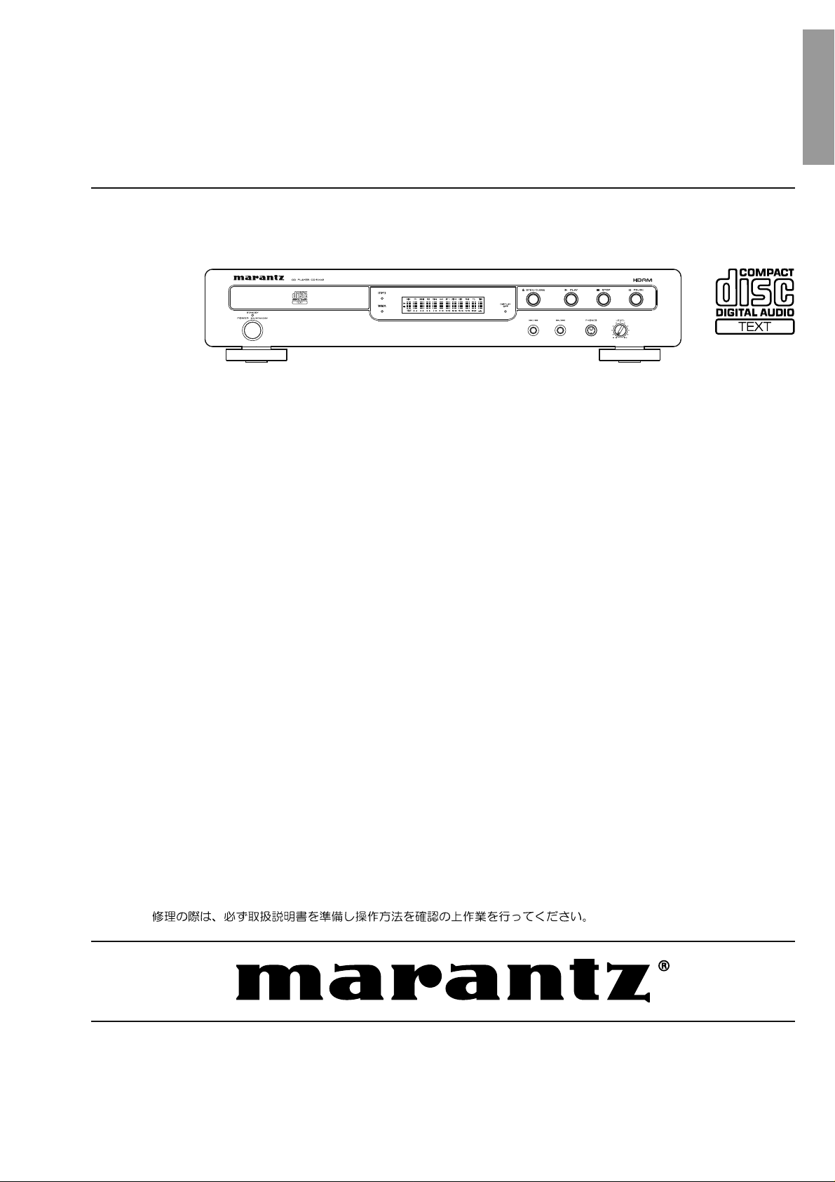
1. TECHNICAL SPECIFICATIONS
Audio characteristics
Channels ........................................................... 2 channels
Frequency response .................................... 2 Hz to 20 kHz
Dynamic range ........................................................ 100 dB
Signal-to-noise ratio ................................................110 dB
Channel separation .....................................110 dB (1 kHz)
Harmonic distortion ....................................0.002% (1 kHz)
Wow & flutter .........................................Precision of quartz
Error correction system ...................Cross-interleave Reed
Solomon code (CIRC)
Audio output ...........................................2.35 V rms, stereo
Headphone output ....18 mW/32 ohms (variable maximum)
Digital output
Coaxial output (pin jack) ......................0.5 Vp-p, 75 ohms
Optical output (square optical connector) ..........-19 dBm
Optical readout system
Laser .............................................. AlGaAs semiconductor
Wavelength ..............................................................780 nm
Signal system
Sampling frequency ...............................................44.1 kHz
Quantization ....................................... 16-bit linear/channel
Power supply
F version .............................................. AC 100 V 50 /60 Hz
K version ...................................................AC 220 V 50 Hz
N version ............................................. AC 230 V 50 /60 Hz
Power consumption .....................................................19 W
Cabinet, etc.
Control in/out ...........................................................RCA jack
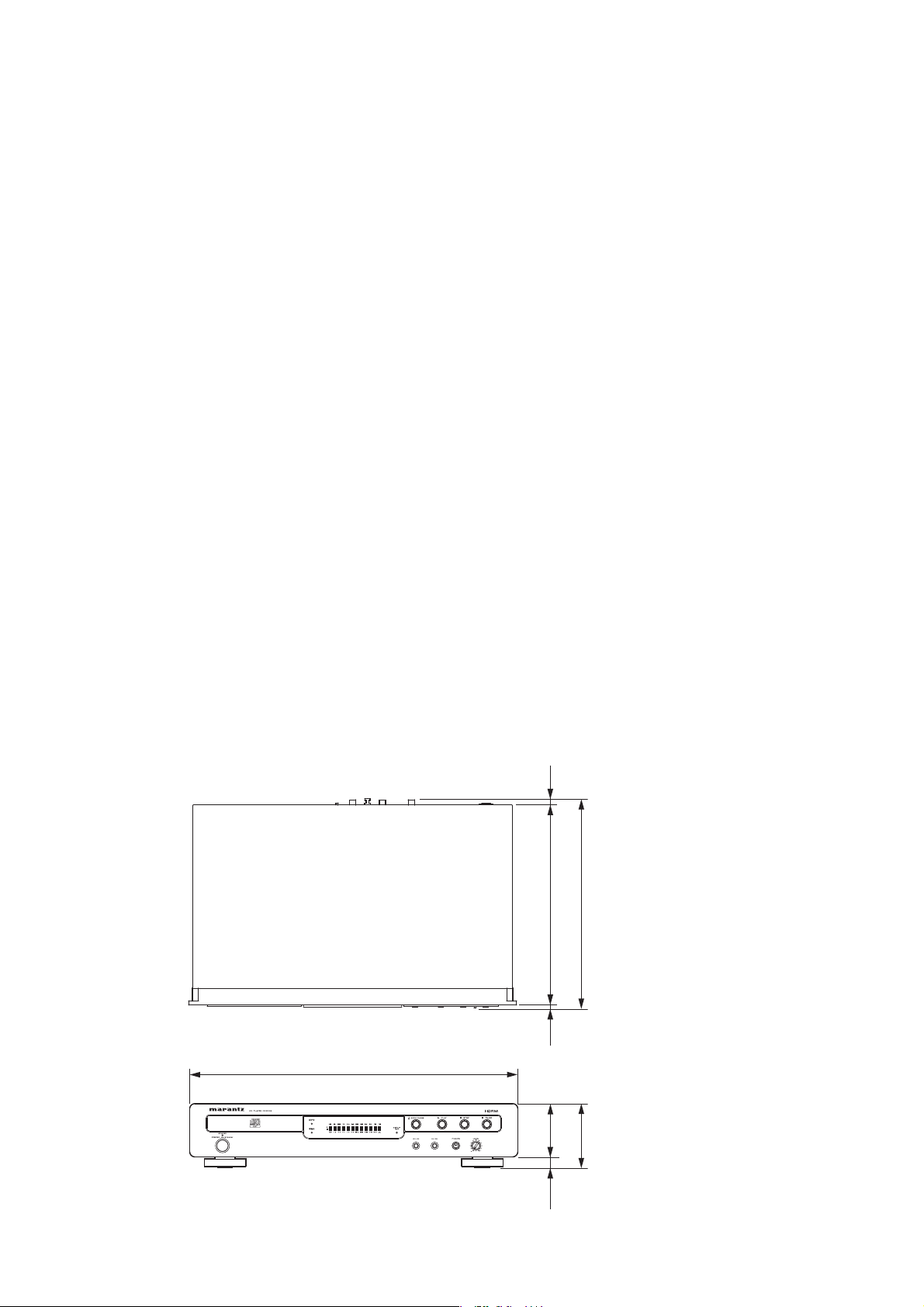
Maximum dimensions ........... 440(W) x 87(H) x 283(D) mm
Weight .......................................................................4.7 kg
Allowable operating temperature .....................+5 to +35 °C
Allowable operating humidity ....... 5 to 90 % (no condensation)
Dimensions (unit: mm)
9269
515 72
440
87 283
1
Page 4
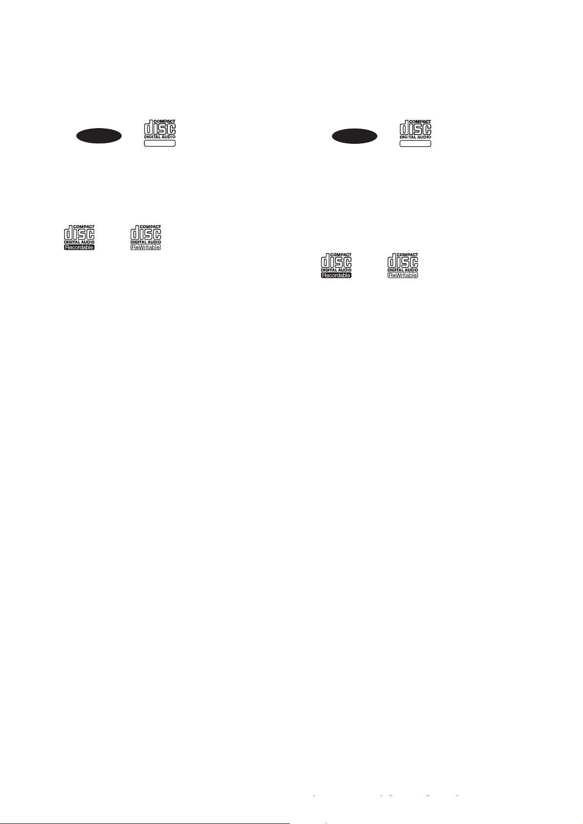
• Supports CD-Text display
CD-Text is an extension to the existing audio CD
standard that enables text information, such as the
name of the artist, album title and song titles to be
stored on an audio CD.
CDs with the following logos support this function.
CD-TEXT 表示対応
¡
CD- T E X T とは従来の音楽 C D にアルバム名、
曲名などの文 字情報を記録した音楽ディスク
です。以 下のようなロゴが付いた CD が対応
しています。
CD TEXT
Text information is recorded on the parts that are not
used in the conventional Audio CDs.
This CD player enables the text information stored
on a CD-Text CD to be read (applies only to English
alphanumeric text).
7
Playing CD-R/CD-RW discs
This unit can play back the CD-RW (ReWritable)
discs as well as ordinary Audio CD and CD-R
(Recordable) discs.
• This unit can play back Audio CD format and CDR/CD-RW discs which contain MP3 music data.
However, some discs may have problems such
as unable to play, noise or sound distortion.
* For details, please read the instruction manual
provided with a CD recorder.
• The CD-R and CD-RW discs should contain
properly-recorded TOC information so that they
can be played back. In CD recorders, the task of
writing TOC information is referred to as finalizing
the disc. Discs that are not finalized cannot be
properly recognized as an Audio CD and played
back by regular CD players and Super Audio CD
players. For details, please read the instruction
manual provided with a CD recorder.
* TOC stands for Table Of Contents and contains
information such as the total number of tracks
and total playing time of the disc.
• This player can only be used to play Audio CDDA format discs or discs on which MP3 or WMA
audio data have been recorded. Do not attempt
to play a disc containing other data, such as a
CD-ROM for PCs, on this unit.
• As the playback of a CD-RW disc necessitates
partial change of the player setup, it may take
longer time for reading the TOC information than
when an Audio CD or CD-R disc is played.
TEXT
CD TEXT
TEXT
これらの文字情報は、従来の音楽 CD では使
用されていなかった部分に記録されています。
本機ではディスクに記 録された文字情報を見
ることができます。(英数字のみに対応してい
ます。)
■CD-R/CD-RW ディスクの再生
について
本 機では従 来のオーディオ CD や CD-R
(Recordable)に加え、CD-RW(ReWritable)
ディスクの再生も可能です。
•本 機は音 楽 CD フォ ーマット、 または
MP3 の音 楽データが記録された CD-R /
CD-RW ディスクを再生することができま
す。ただし、ディスクによっては「再生で
きない」、「ノイズが出る」、または「音が歪
む」などが起きることがあります。詳しく
はレコーダーの取扱説明書をご覧くださ
い。
•CD-R や CD-RW の再生には必ず TOC*
が正しく記録されていることが必 要です。
CD レコーダーでは TOC 情報を書き込む
ことをファイナライズ(Finalize)といい、
この作業が正常に完了していないディスク
は、通常の CD プレーヤーでは音楽 CD と
して正しく認識されず再生することができ
ませんので十分ご注意ください。詳しくは
CD レコーダーの取扱説明書をご覧くださ
い。
*TOC(トック)とはTableOfContentsの略で、
ディスクの総曲数や総演奏時間などの目次 情
報のことです。
•再生できるのは音楽用の CD-DA フォ ー
マットまたは MP3 / WMA の音楽データ
で記録されたディスクのみです。その他の
データが記録されたディスクは再生しない
でください。
• CD-RW ディスクを再生する場合、プレー
ヤーの設定を一部変更するため、音楽 C D
や CD- R に比べ TOC の読み込みに時間が
かかることがあります。
■MP3/WMA ファイルの再 生に
ついて
本機は MP3(MPEGAudioLayer3)または
WMA(Windows MediaAudio)ファイル形式
で記録されたデータファイルを CD-R、CD-RW
に書き込んだディスクでの再生が可能です。
また、MP3 の I D3 タグに対応しており、ID3 タ
グ情報が記録されているファイルではトラック
2
Page 5

7
Playing MP3 or WMA fi les
This CD player can be used to play CD-R or CD-RW
discs on which MP3 (MPEG Audio Layer-3) or WMA
(Windows Media Audio) format audio files have
been recorded.
Support for MP3 ID3 tags enables display of ID3
information, such as artist names, album titles,
track titles and the like, if this information has been
recorded with the tracks.
• Windows Media and the Windows Logo are the
registered trademark and trademark of Microsoft
Corporation in the United States and other
countries.
• Music that you have recorded that is subject
to copyright laws is for personal use only, and
cannot be used otherwise without the permission
of the copyright holder.
Caution:
• The sound file specification supported by this
CD player is “MPEG-1 Audio Layer-3” (sampling
frequency fs 32 kHz, 44.1 kHz, 48 kHz). Other
specifications, such as MPEG-2 Audio Layer-3,
MPEG-2.5 Audio Layer-3, MP1 or MP2 are not
supported.
• Generally the higher the bit rate, the higher the
sound quality.
MP3 bit rates are between 32 - 320 kb/s and for
WMA between 64 - 160 kb/s. It is recommended
that MP3/WMA recordings with a bit rate of at
least 128 kb/s be used.
• The text information, such as ID3 tag information
and file names that are displayed during
playback of MP3s, support English alphanumeric
characters only.
• When playing variable bit rate files, it is possible
that the playing time may not be displayed
accurately.
• When writing onto CD-R or CD-RW discs,
please use either ISO9660 mode 1 or ISO9660
mode 2-disc format. Multi-session recording is
also supported enabling the playing of data that
have been added to a disc.
• MP3/WMA files that have been recorded by
“packet writing” cannot be played back.
• Depending on the condition of the recorded data,
it may take some time to read song information.
• In the case of an Enhanced or Mixed Mode CD
having combined audio format CD-DA along with
MP3/WMA files, only the CD-DA audio portion
will be played.
• The playback of WMA DRM (Digital Rights
Management) files is not supported by this
player.
タイトル、アーティスト名、アルバムタイトル
などを表示することができます。
•WindowsMedia,Windows ロ ゴ は
米国、その他の国で、米国 Microsoft
Corporation の登録商標または商標です。
• お客様が録音したものは個人として楽しむ
などのほかは著作権法上、権利者に無断で
使用できません。
•本 機で対応している規 格は MPEG-1
Audio Layer-3(サンプリング周波数fs
は 32、44.1、48k Hz)です。 それ以 外の
MPEG-2 Audio Layer-3、MPEG-
2.5AudioLayer-3 および MP1、MP2 な
どには対応していません。
• 一般にビットレートが高いほど音質が良く
なります。
MP3 の対 応ビットレートは 32 〜 320
kbps、WMA は 64 〜 160kbps です。本
機では 128kbps 以上のビットレートで記
録された MP3 / WMA のご使用をおすす
めします。
•MP3/WMA ファイルには必ず拡 張 子
.MP3.WMA を付けてください。
.MP3.WMA 以外の拡張子を付け
た場合や拡張子を付けなかった場合はファ
イルを再生できません。
• プレイリストには対応していません。
•ディスク 1 枚あたりの再 生 出 来るファイ
ル数は最大 255 で、フォルダー数は最大
255 です。
• 本機は 32 文字までのフォルダ名やファイ
ル名を表示できます。
•本機は、MP3ID3 タグに対応しています。
• MP3 を再生した時に表示される ID3 タグ
情報やファイル名の文字情報は日本語表示
に対応していません。英数字をご使用くだ
さい。
• 可変ビットレートファイルの再生時には、
正しく時間表示されないことがあります。
•CD-R や CD-RW に書き込むフォーマット
は ISO9660 モード 1 またはモード 2 で書
き込みをしてください。また、マルチセッ
ションに対応していますので、追加で書き
込みしたデータの再生もできます。
•パケットライトで記 録された MP3/
WMA ファイルは再生できません。
•
記録したデータの状態によっては曲情報を
読み取るのに時間がかかる場合があります。
• 音楽用のフォーマット CD-DA と MP3 /
WMA ファイルが混在したエンハンスド
CD およびミックス CD は、音楽用のフォー
マット CD-DA のみ再生します。
•WMADRM(著作権保護)ファイルの再生
には対応していません。
3
Page 6
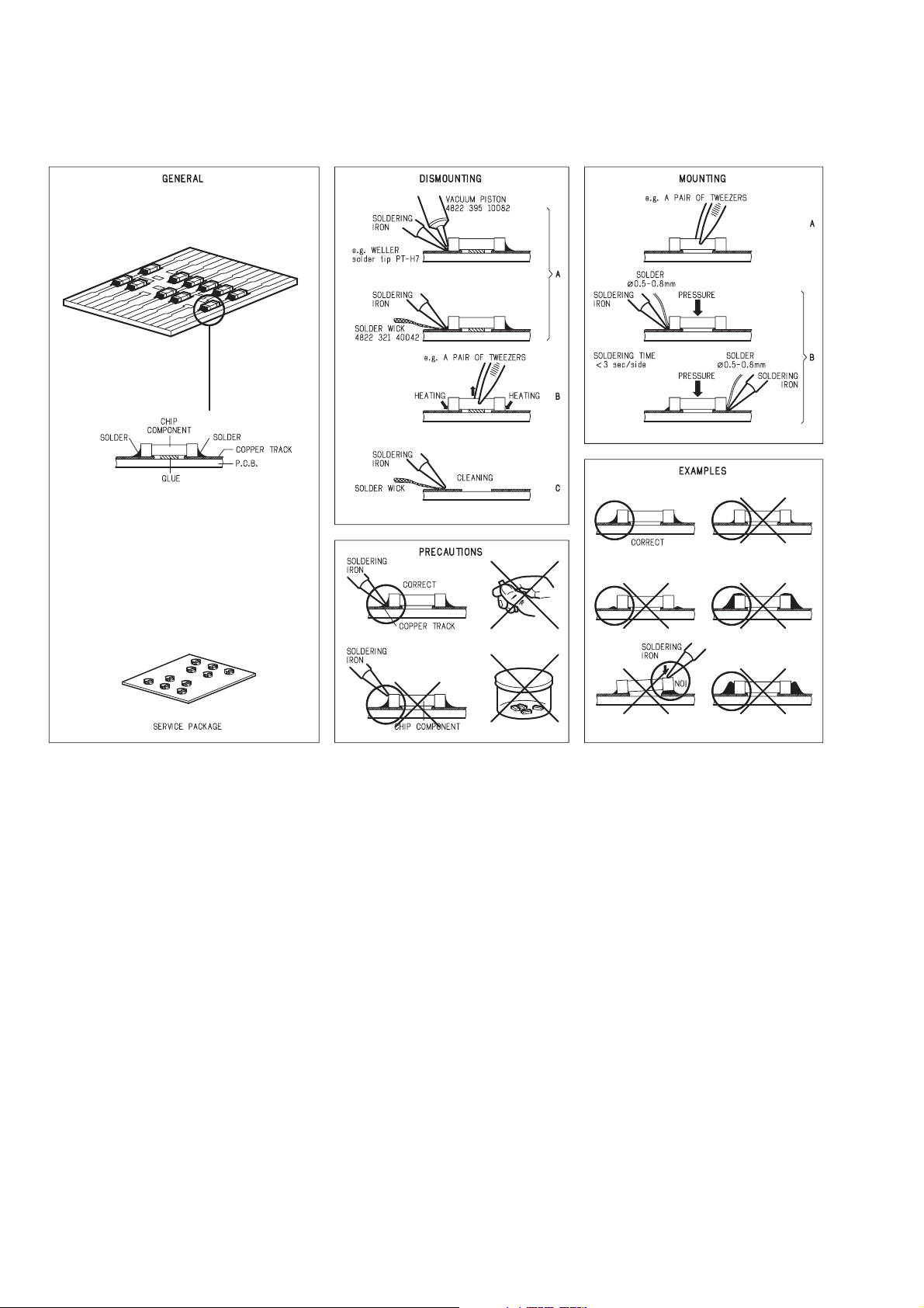
2. SERVICE HINTS AND TOOLS
SERVICE HINTS
SERVICE TOOLS
Audio signals disc 4822 397 30184 or TCD-784
Disc without errors +
Disc with DO errors, black spots and fingerprints 4822 397 30245 (SBC444A) or TCD-726
Disc (65 min 1kHz) without no pause 4822 397 30155
Max. diameter disc (58.0 mm) 4822 397 60141
Torx screwdrivers
Set (straight) 4822 395 50145
Set (square) 4822 395 50132
13th order filter 4822 395 30204
DVD test disc (PAL) 4822 397 10131
DVD test disc (NTSC) ALMEDIO TDV-540
4
070703MZ
Page 7
3. WARNING AND LASER SAFETY INSTRUCTIONS
F
ATTENTION
Tous les IC et beaucoup d’autres semiconducteurs sont sensibles aux décharges
statiques (ESD).
Leur longévité pourrait être considérablement
écourtée par le fait qu’aucune précaution
n’est prise a leur manipulation.
Lors de réparations, s’assurer de bien être
relié au même potentiel que la masse de
l’appareil et enfiler le bracelet serti d’une
résistance de sécurité.
Veiller a ce que les composants ainsi que les
outils que l’on utilise soient également a ce
potentiel.
D
WARNUNG
Alle IC und viele andere Halbleiter sind
empfindlich gegen elektrostatische
Entladungen (ESD).
Unsorgfältige Behandlung bei der Reparatur
kann die Lebensdauer drastisch vermindern.
Sorgen sie dafür, das Sie im Reparaturfall
über ein Pulsarmband mit Widerstand mit
dem Massepotential des Gerätes verbunden
sind.
Halten Sie Bauteile und Hilfsmittel ebenfalls
auf diesem Potential.
WAARSCHUWING
Alle IC’s en vele andere halfgeleiders zijn
gevoelig voor elektrostatische ontladingen
(ESD).
Onzorgvuldig behandelen tijdens reparatie
kan de levensduur drastisch doen
verminderen.
Zorg ervoor dat u tijdens reparatie via een
polsband met weerstand verbonden bent met
hetzelfde potentiaal als de massa van het
apparaat.
Houd componenten en hulpmiddelen ook op
ditzelfde potentiaal.
AVVERTIMENTO
Tutti IC e parecchi semi-conduttori sono
sensibili alle scariche statiche (ESD).
La loro longevita potrebbe essere fortemente
ridatta in caso di non osservazione della piu
grande cauzione alla loro manipolazione.
Durante le riparazioni occorre quindi essere
collegato allo stesso potenziale che quello
della massa dell’apparecchio tramite un
braccialetto a resistenza.
Assicurarsi che i componenti e anche gli
utensili con quali si lavora siano anche a
questo potenziale.
All ICs and many other semi-conductors are
susceptible to electrostatic discharges (ESD).
Careless handling during repair can reduce
life drastically.
When repairing, make sure that you are
connected with the same potential as the
mass of the set via a wrist wrap with
resistance.
Keep components and tools also at this
potential.
WARNING
Safety regulations require that the set be restored to its original condition
and that parts which are identical with those specified be used.
Veiligheidsbepalingen vereisen, dat het apparaat in zijn oorspronkelijke
toestand wordt terug gebracht en dat onderdelen, identiek aan de
gespecifieerde worden toegepast.
Bei jeder Reparatur sind die geltenden Sicherheitsvorschriften zu beachten.
Der Originalzustand des Gerats darf nicht verandert werden.
Fur Reparaturen sind Original-Ersatzteile zu verwenden.
Le norme di sicurezza esigono che l’apparecchio venga rimesso nelle
condizioni originali e che siano utilizzati pezzi di ricambiago idetici a quelli
specificati.
Les normes de sécurité exigent que l’appareil soit remis a l’état d’origine et
que soient utilisées les pièces de rechange identiques à celles spécifiées.
“Pour votre sécurité, ces documents
doivent être utilisés par des
spécialistes agrées, seuls habilités à
réparer votre appareil en panne.”
GB
NL
I
D
I
F
GB
NL
LASER SAFETY
CAUTION VISIBLE AND INVISIBLE LASER RADIATION WHEN OPEN AVOID EXPOSURE TO BEAM
ADVARSEL SYNLIG OG USYNLIG LASERSTRÅLING VED ÅBNING UNDGÅ UDS
Æ
TTELSE FOR STRÅLING
ADVARSEL SYNLIG OG USYNLIG LASERSTRÅLING NÅR DEKSEL Å PNES UNNGÅ EKSPONERING FOR STRÅLEN
VARNING SYNLIG OCH OSYNLIG LASERSTRÅLNING NÄR DENNA DEL ÄR ÖPPNAD BETRAKTA EJ STRÅLEN
VARO! AVATT AESSA OLET ALTTIINA NÄKYVÄLLE JA NÄKYMÄTTÖMÄLLE LASER SÄTEILYLLE. ÄLÄ KATSO SÄTEESEEN
VORSICHT SICHTBARE UND UNSICHTBARE LASERSTRAHLUNG WENN ABDECKUNG GEÖFFNET NICHT DEM STRAHL AUSSETSEN
DANGER VISIBLE AND INVISIBLE LASER RADIATION WHEN OPEN AVOID DIRECT EXPOSURE TO BEAM
ATTENTION RAYONNEMENT LASER VISIBLE ET INVISIBLE EN CAS D'OUVERTURE EXPOSITION DANGEREUSE AU FAISCEAU
USE OF CONTROLS OR ADJUSTMENTS OR PERFORMANCE OF PROCEDURE OTHER THAN THOSE
SPECIFIED HEREIN MAY RESULT IN HAZARDOUS RADIATION EXPOSURE.
AVOID DIRECT EXPOSURE TO BEAM
WARNING
The use of optical instruments with this product will increase eye hazard.
Repair handling should take place as much as possible with a disc loaded inside the player
WARNING LOCATION: INSIDE ON LASER COVERSHIELD
This unit employs a laser. Only a qualified service person should remove the cover or attempt to service this
device, due to possible eye injury.
030804ecm
5
Page 8
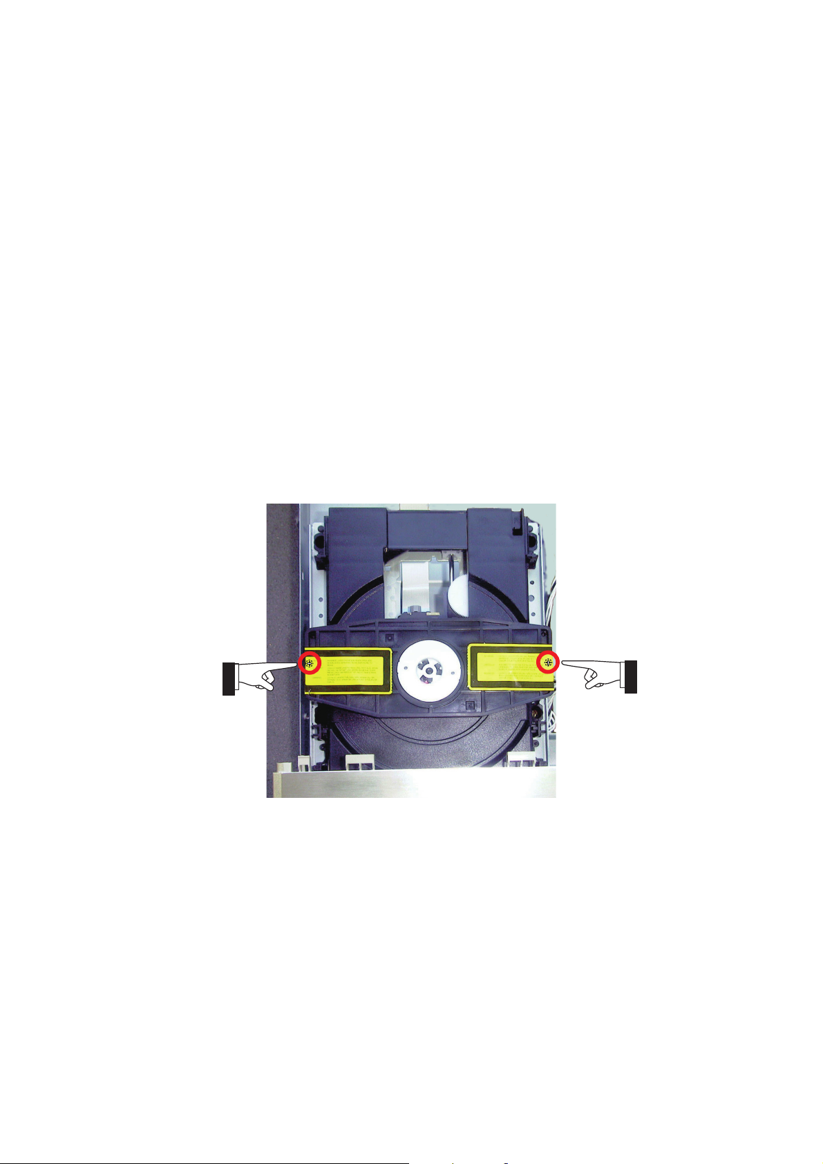
4. SERVICE MODE AND TAKING THE DISC
OUT OF EMERGENCY
[A] SERVICE MODE
1. Insert mains cable plug in the outlet and press POWER
button.
2. Press the OPEN/CLOSE button to open the tray.
3. Press the g/i button for about five seconds.
4. The version number of the microprocessor is displayed
Ex. : 2007 - 06 - 25 - 1
5. Press the j/\h button for about five seconds.
6. Light up all the FL segment.
Turn off power to quit Service mode.
[B] TAKING THE DISC OUT OF EMERGENCY
1. Remove the top cover of the player.
2. Remove 2 screws under the label shown in the picture
follows.
3. Remove the disc clamper.
4. Now you can remove the disc.
Remove those screws
6
Page 9
5. UPDATE MICROPROCESSOR SOFTWARE
PROCEDURE
When microprocessor software was updated, update the
software in the following procedure.
5. UPDATE MICROPROCESSOR SOFTWARE
PROCEDURE
マイコンのソフトウェアが更新された場合、下記の手順に従っ
てアップデートしてください。
Necessary Equipment
• Windows PC (OS: Windows2000 or WindowsXP) with
Serial port.
• RS-232C Dsub-9 pin cable (female to female/straight
type).
• Connection JIG (90M-SR4500JIG)
• Update tool (FlashProg.exe, other files and folders in
Flash Programmer folder)
• Update data (CD6002_yymmdd_x.s24)
NOTE : The yy is two digits of year. The mm is month. The
dd is date. The x is release number.
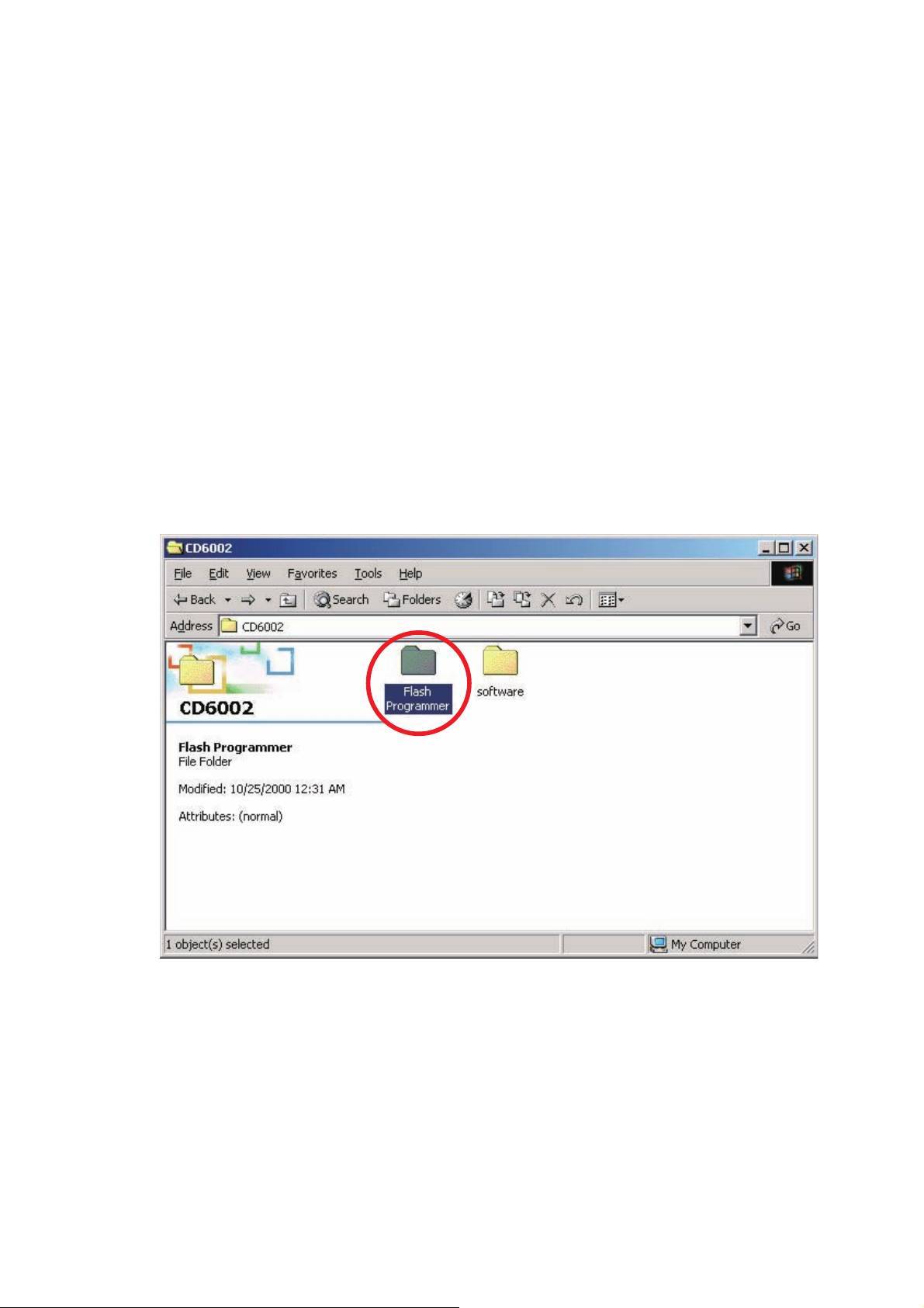
[A] Update Procedure
1. Put the "Flash Programmer" and "software" folder into
anywhere on your PC’s hard disc.
2. Double click the "Flash Programmer" folder.
必要機器
• Windows PC (OS: Windows2000またはWindowsXP) で
Serialポートのあるもの
• RS-232Cストレートケーブル (9pinメス−9pinメス)
•
接続冶具 (90M-SR4500JIG)
•
アップデート用書き込みソフトウェア (Flash
Programmer
イルとフォルダ
•
アップデート用データ (CD6002_yymmdd_x.s24)
注意 : yyは年の下二桁、mmは月、ddは日、xはリリースナン
バー
フォルダ内 FlashProg.exe、および他のファ
)
[A] Update Procedure
1. "Flash Programmer"と"software"フォルダをPCの任意のフ
ォルダにコピーします。
2. "Flash Programmer"フォルダをダブルクリックします。
7
Page 10
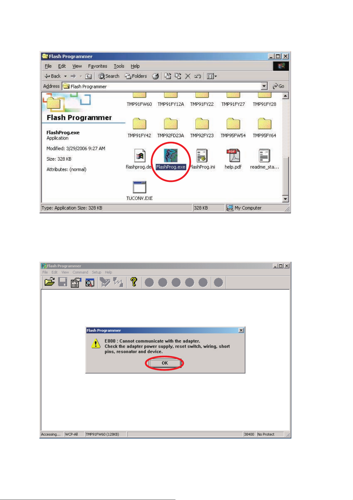
3. Double click FlashProg.exe, and launch the Flash
Programmer.
3. FlashProg.exeをダブルクリックし、Flash Programmerを
起動します。
NOTE : When a Flash Programmer does not launch even if
double-clicked FlashProg.exe, please refer to "[B]
When a Flash Programmer did not launch".
4. Click OK.
: FlashProg.exeをダブルクリックしてもFlash
注意
Programmer
Programmer did not launch"
が起動しない場合は、"[B] When a Flash
を参照してください。
4. OKをクリックします。
NOTE : Since Flash Programmer communicates with the
unit automatically, the following dialog box appears
when it fails in communication.
注意
: は本機に自動的に通信接続を行います。このダイアログ
ボックスは通信接続に失敗すると常に表示されます。
8
Page 11
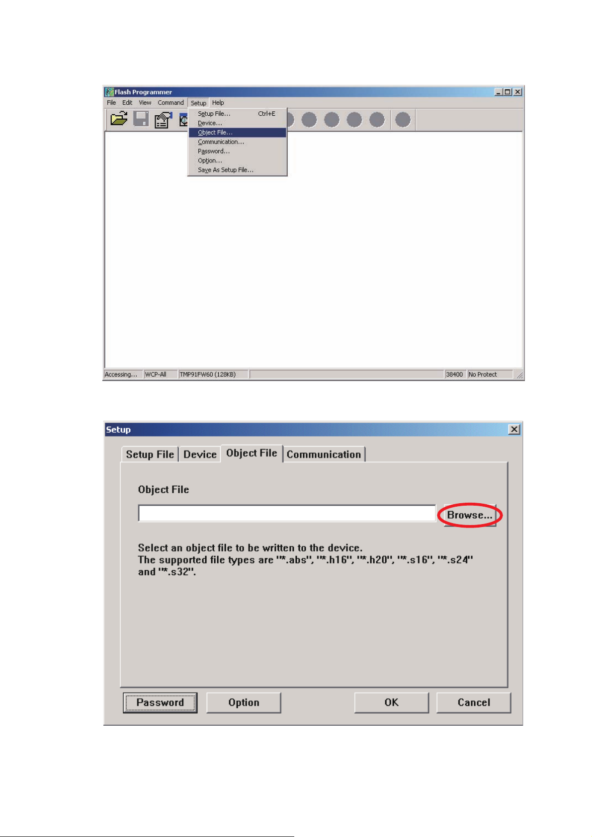
5. Click the Setup in the menu bar and select the Object
file.
5. メニューバーからSetupをクリックし、Object fileを選択
します。
6. Click Browse.
6. Browseをクリックします。
9
Page 12
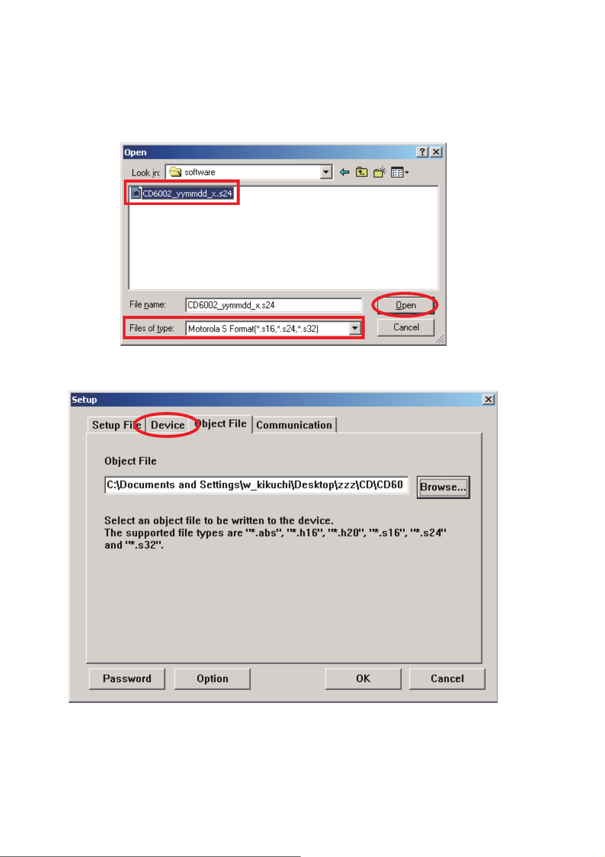
7. Choose the Motorola S Format(*.s16,*.s24,*.s32) in
Files of type.
Choose the
CD6002_yymmdd_x.s24, and click Open.
NOTE : The yy is two digits of year. The mm is month. The
dd is date. The x is release number.
7. Files of type をMotorola S Format(*.s16,*.s24,*.s32)に
変更します。
CD6002_yymmdd_x.s24を選択し、Openをクリックし
ます。
注意
: yyは年の下二桁、mmは月、ddは日、xはリリースナン
バー
8. Click Device tab.
8. Deviceタブをクリックします。
10
Page 13
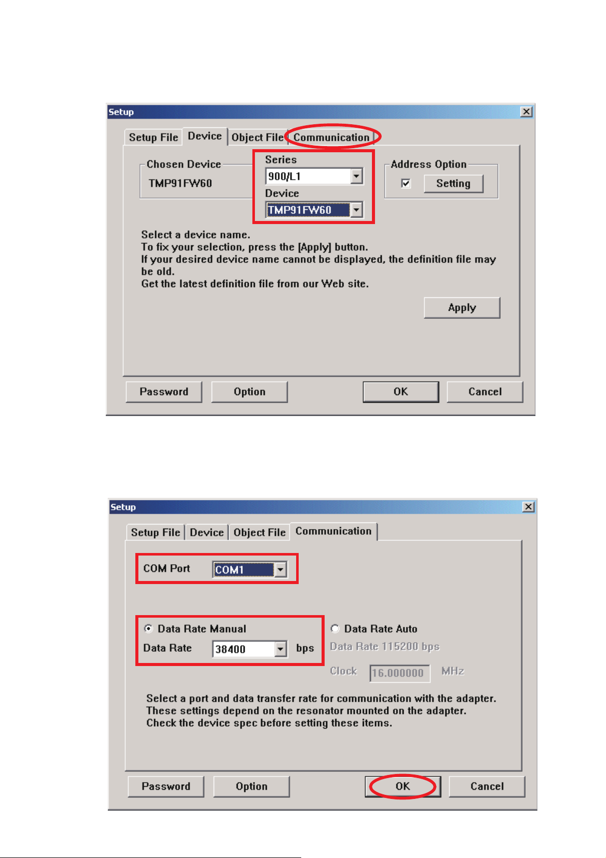
9. Choose the TMP91FW60 in the Device, and choose the
900/L1 in the Series.
And click Communication tab.
9. DeviceからTMP91FW60を選び、Seriesから900/L1を選択
します。
そして、
Communicationタブをクリックします。
10. Choose the Serial port number in the COM Port.
Check the Data Rate Manual, and choose the 38400 in
the Data Rare.
And Click OK.
10. COM Portから使用するポート番号を選択します。
Data Rate Manualにチェックを入れ、Data Rareから
38400を選択します。
OKをクリックします。
11
Page 14
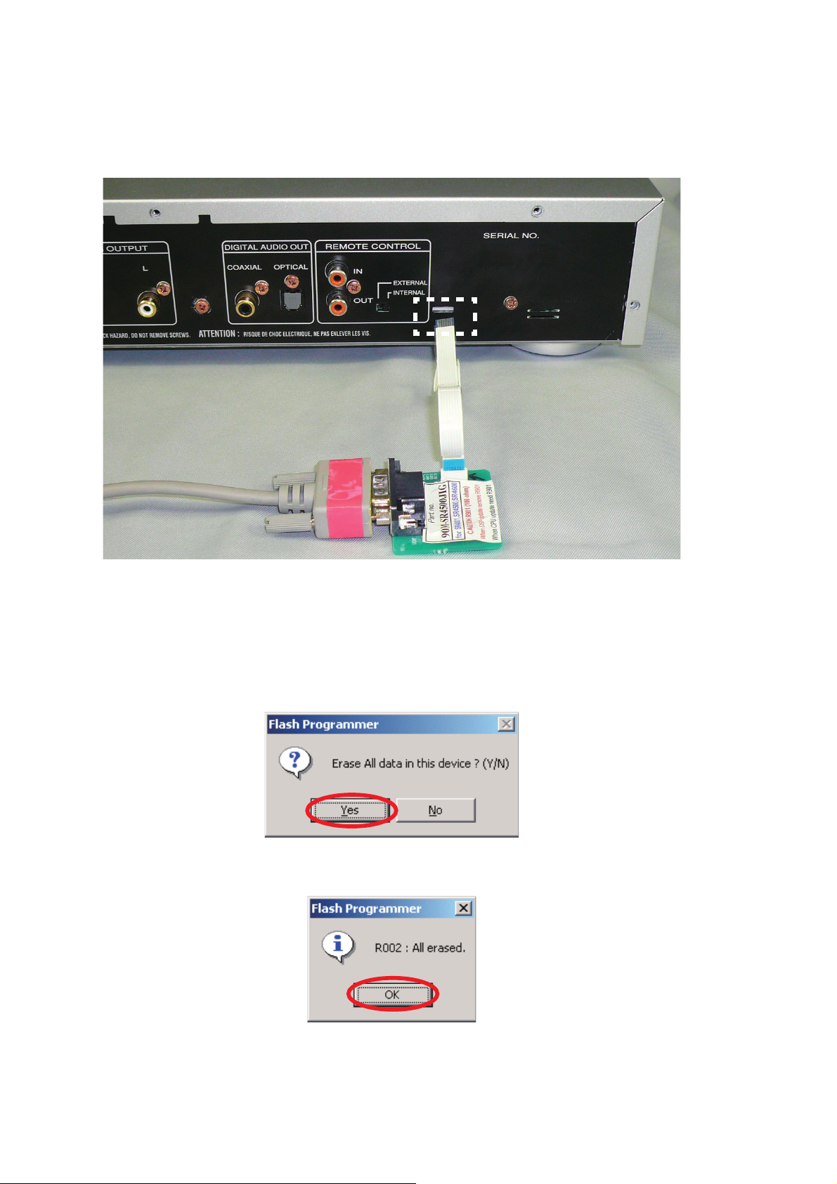
11. Disconnect the mains cord from the unit.
12. Connect the RS-232C on the connection JIG and the
Serial Port of windows PC with RS-232C cable.
13. Connect FFC (upside contact) to the rear panel of the
unit from connection JIG.
11. 本機から電源ケーブルを外します。
12. 接続冶具のRS-232C端子とPCのSerialポートをRS-
232C
ケーブルで接続します。
13. 本機のリアパネルに接続冶具のFFC をコンタクト面を上に
して差し込みます。
14. Connect the mains cord into the unit.
15. If the connection with the Flash Programmer is
successfully made, a dialogue box saying "Erase All
data in this devise? (Y/N)" appears automatically. If the
connection fails, error message will appear. (Ex.: E000)
Click Yes.
16. Click OK.
14. 本機に電源ケーブルを接続します。
15. Flash Programmerが通信接続に成功すると"Erase All data
in this devise? (Y/N)"
的に表示されます。接続に失敗するとエラーメッセージが
表示されます。(例:
と書かれたダイアログボックスが自動
E000)
Yesをクリックします。
16. OKをクリックします。
12
Page 15
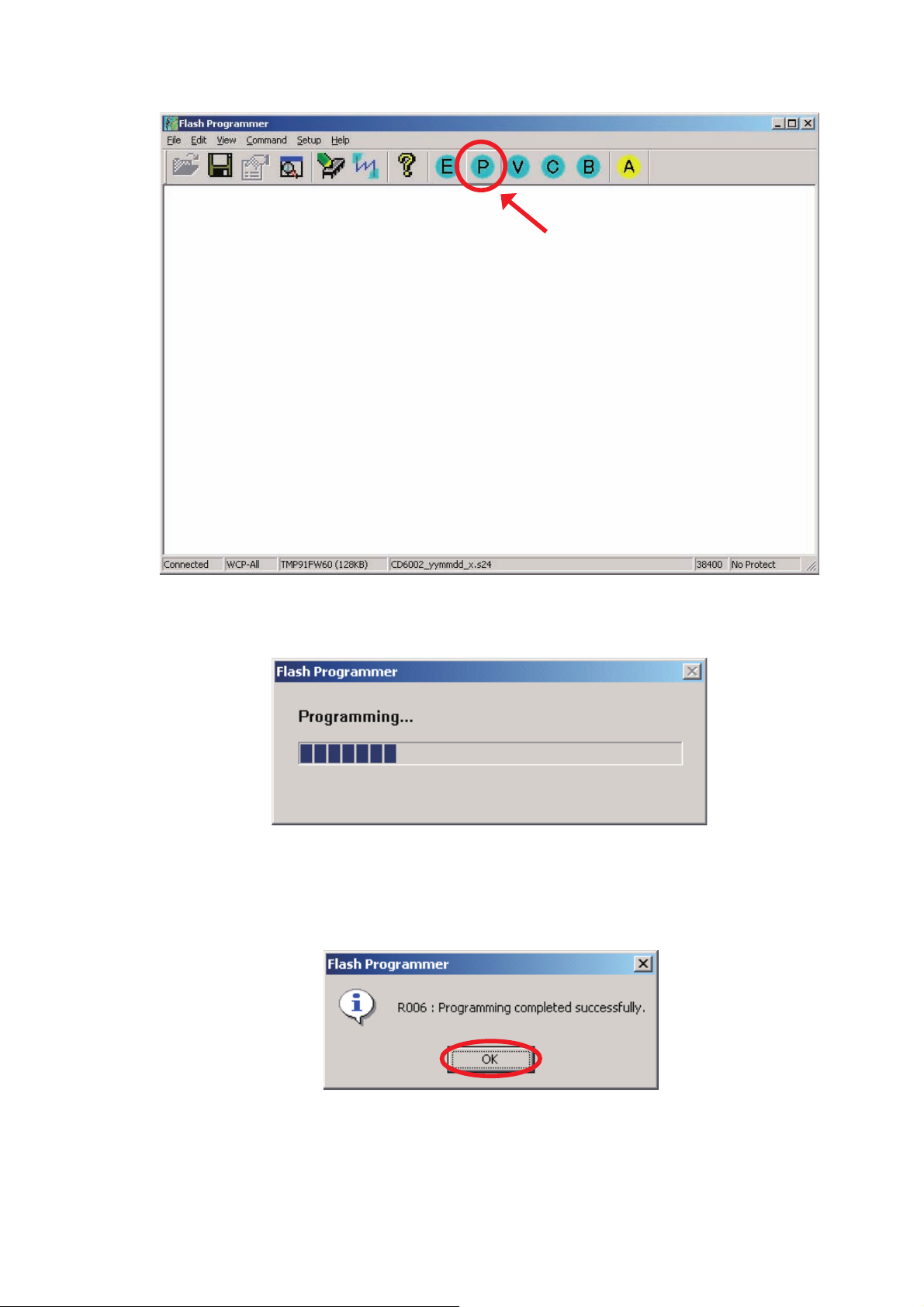
17. Click P (Program) to start update.
17. P (Program)をクリックし、アップデートを開始します。
18. Software is written into the microprocessor.
The writing of software takes about 50 seconds.
19. If the software is updated successfully, a dialog box
saying "R006: Programming completed successfully."
appears.
Click OK.
18. ソフトウェアがマイコンに書き込まれます。
ソフトウェアの書き込みにかかる時間はおよそ
50秒です。
19. アップデートが完了すると"R006: Programming
completed successfully"
表示されます。
と書かれたダイアログボックスが
OKをクリックします。
13
Page 16
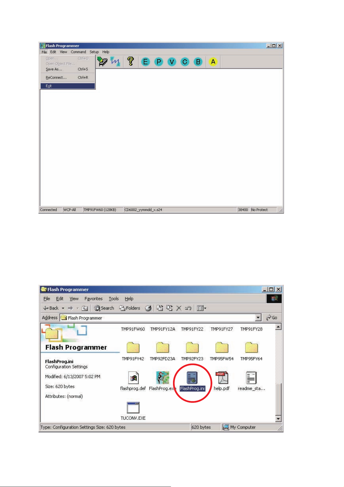
20. Click the File in the menu bar and select the Exit.
20. メニューバーのFileをクリックし、Exitを選択します。
21. Disconnect mains cord from the unit, and then disconnect
FFC of connection JIG from the unit.
[B] When a Flash Programmer did not launch
1. Open the FlashProg.ini in the Flash Programmer folder
by text editor. (EX.: Notepad, etc)
21. 電源ケーブルを本機からはずし、その後接続冶具のFFCを
本機から外します。
[B] When a Flash Programmer did not launch
1. Flash Programmerフォルダ内のFlashProg.iniをテキスト
エディタで開きます。(メモ帳など)
14
Page 17
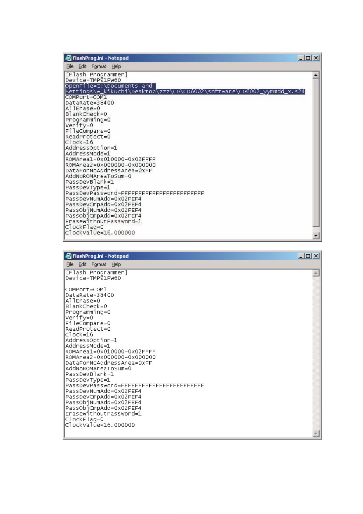
2. Delete the text "OpenFile=C:\...(your PC setting)...\???.
s24".
2. テキスト文のOpenFile=C:\...(PC環境により異なりま
す。
)...\???.s24を削除します。
15
Page 18

3. Save the FlashProg.ini.
3. FlashProg.iniを上書き保存します。
4. Close the text editor.
4. テキストエディタを閉じます。
5. Probably you can launch the Flash Programmer. Go to
the [A] Update Procedure step 3.
5. これでFlash Programmerを起動することが出来ますので
[A] Update Procedure手順3に戻ってください。.
16
Page 19

6. WIRING DIAGRAM
MAIN PWB
POWER PWB
MAIN TRANSF.
MAINS
SUB TRANSF.
CD MECHANISM
TACT SW PWB
H/P(HEADPHONE)
PWB
FRONT PWB
17 18
Page 20

7. BLOCK DIAGRAM
CD-RF
(Audio Out)
CD-RF
IN
Amp
Audio
DAC
Analog
Post
Filter
3.3V 1.5V
Servo
ADC
CDP
DSP
24-Bit
DSP
1Mbit
SRAM
Servo
Processor
Servo
DAC
Peripheral
I/F
PLL/VCO
MAIN TRANSF.
SUB TRANSF.
2019
Page 21

8. SCHEMATIC DIAGRAM
MAIN PWB 1/2
DSP & PITCH PART
TO/FROM
CD MECHANISM
TO/FORM
UPDATE
TO/FROM
CD MECHANISM
TO/FROM
CD MECHANISM
TO/FROM
FRONT PWB
TO
MAIN PWB 2/2
TO
MAIN PWB 2/2
OPTICAL
COAXIAL
REMOTE
CONTROL
21 22
Page 22

MAIN PWB 2/2
AUDIO PART
FROM
MAIN PWB 1/2
L
FROM
MAIN PWB 1/2
R
POWER SUPLLY PART
HEADPHONE PWB
4.7K
4.7K
75
75
75
75
TO/FROM
FRONT PWB
MAINS CORD
POWER PWB
HEADPHONE
2423
Page 23

TACT SW PWB
FRONT PWB
TO/FROM
MAIN PWB 2/2
TO/FROM
MAIN PWB 12
25 26
Page 24

鉛フリー半田
9. PARTS LOCATION
FRONT A
Q202 Q203
Q204
鉛フリー半田
半田付けには、鉛フリー半田
POWER A PWB
(Sn-Ag-Cu)
を使用してください。
Q951
POWER B PWB
Lead-free Solder
When soldering, use the Lead-free Solder (Sn-Ag-Cu).
2827
Page 25

FRONT B
鉛フリー半田
IC21
TACT SW A
Q201
TACT SW B
HEADPHONE A PWB
Q801 - Q804
HEADPHONE B PWB
IC81
29 30
鉛フリー半田
半田付けには、鉛フリー半田
(Sn-Ag-Cu)
を使用してください。
Lead-free Solder
When soldering, use the Lead-free Solder (Sn-Ag-Cu).
Page 26

MAIN A PWB
鉛フリー半田
IC31
Q301 IC96 IC95
IC45 IC46
IC48 IC47
IC49 IC50
IC51
IC52
Q502IC53
Q374 Q503
IC32
IC33
Q718-Q720 Q618-Q620
Q716 Q715
Q714 - Q709
Q708 Q707
Q705 Q704
Q702 Q703 Q701
Q717 Q617
Q706
Q616 Q615
IC41
IC92
Q903 Q911
Q910
Q614 - Q609
Q608 Q607
Q606
Q605 Q604
Q602 Q603 Q601
IC93 Q904 - Q906
IC91
Q909
IC94
Q908
鉛フリー半田
半田付けには、鉛フリー半田
(Sn-Ag-Cu)
を使用してください。
Lead-free Solder
When soldering, use the Lead-free Solder (Sn-Ag-Cu).
3231
Page 27

MAIN B PWB
鉛フリー半田
33 34
鉛フリー半田
半田付けには、鉛フリー半田
(Sn-Ag-Cu)
を使用してください。
Lead-free Solder
When soldering, use the Lead-free Solder (Sn-Ag-Cu).
Page 28

10. EXPLODED VIEW AND PARTS LIST
33
/F only
/N only
/K, /U only
S8
S1
S10
X5
S1
S8
S2
S8
S7
32
19
S7
S1
BK31
20
MECHA LOADER
AND TRAVERSE
S8
S7
27
MAIN PWB
S7
S8
31
S7
24
25
TACT SW PWB
10
9
S4
8
S8
X3
S3
7
S2
21
S8
18
6
17
FRONT PWB
X5
S4
24
28
S8
29
X3
x4
S5
S8
1
13
12
2
S10
X5
11
14
X2
S4
22
30
34
22
15
HEADPHONE PWB
24
23
23
X2
S6
POWER PWB
BK81
X2
S6
S8
3
5
CTBD3+8JFB
4
S9
S10
X5
X4
S10
CTB3+10JFB
S9
S8
CTW3+18JR
S7
CTW3+8JR
S6
CTB4+6FFZR
S5
CTB3+10JR
S4
CTS3+8JR
S3
CTB4+6FFZR
S2
CTB4+6FFC
CTB3+8JFBS1SCREW
NO.
PARTS NO.
SCREW
SCREW
SCREWCTB3+6JR
SCREW
SCREW
SCREW
SCREW
SCREW
SCREW(BLACK Ver.)
SCREW(GOLD Ver.)
SCREW(SILVER Ver.)
DESCRIPTION
3635
Page 29

P.C.B.
(
)
(MZ)
p
p
/
p
/
/
p
p
/
p
/
/
p
p
/
p
/
/
p
p
/
p
/
/
p
p
/
p
/
/
p
p
/
p
/
/
p
p
/
p
/
/
p
p
/
p
/
/
pnsp
p
p
/
p
/
/
pnsp
pnsp
p
p
/
p
/
/
pnsp
pnsp
/
pnsp
/
pnsp
/
pnsp
pnsp
pnsp
pnsp
p
p
/
p
/
NAME
POS. NO.
VERS.
COLOR
1F B ns
1F N ns
K1G ns
1
N1B 00M24AW251010 00M24AW251010 BADGE NEW MZ BADGE CGB1A117
1
N1S 00M24AW251020 00M24AW251020 BADGE NEW MZ BADGE SILVER CGB1A117G
1
2F B ns
2F N ns
K1G ns
2
N1B 00M30CW053010 00M30CW053010 ESCUTCHEON ORNAMENT DOOR BLACK CGR1A427ZH10
2
N1S 00M30CW053210 00M30CW053210 ESCUTCHEON ORNAMENT DOOR SILVER CGR1A427R6YH51
2
3F B ns
3F N ns
K1G ns
3
N1B 00M30CW158010 00M30CW158010 WINDOW WINDOW BLACK/GOLD CGU1A405Z
3
N1S 00M30CW158210 00M30CW158210 WINDOW WINDOW SILVER CGU1A405Y
3
4F B ns
4F N ns
K1G ns
4
N1B 00M30CW053020 00M30CW053020 ESCUTCHEON ORNAMENT KNOB BLACK CGR1A428ZH10
4
N1S 00M30CW053220 00M30CW053220 ESCUTCHEON ORNAMENT KNOB SILVER CGR1A428R6YH51
4
5F B ns
5F N ns
K1G ns
5
N1B 00M24AW154010 00M24AW154010 KNOB KNOB LEVEL BLACK CBN1A170 CBN1A170K92
5
N1S 00M24AW154210 00M24AW154210 KNOB KNOB LEVEL SILVER CBN1A170 CBN1A170R6G13
5
6F B ns
6F N ns
K1G ns
6
N1B 00M30CW248010 00M30CW248010 PANEL FRONT AL PANEL CKM1A185ZC23
6
N1S 00M30CW248210 00M30CW248210 PANEL FRONT AL PANEL CKM1A185YC40
6
7F B ns
7F N ns
K1G ns
7
N1B 00M30CW105020 00M30CW105020 CHASSIS PANEL SUB BLACK CGW2A410R4K92
7
N1S 00M30CW105220 00M30CW105220 CHASSIS PANEL SUB SILVER CGW2A410R6G13
7
PART NO.
FOR EUR
PART NO.
PART NAME DESCRIPTION
00M24AW251010 BADGE NEW MZ BADGE CGB1A117
00M24AW251010 BADGE NEW MZ BADGE CGB1A117
00M24AW251010 BADGE NEW MZ BADGE CGB1A117
00M30CW053010 ESCUTCHEON ORNAMENT DOOR BLACK CGR1A427ZH10
00M30CW053110 ESCUTCHEON ORNAMENT DOOR GOLD CGR1A427RFYH40
00M30CW053110 ESCUTCHEON ORNAMENT DOOR GOLD CGR1A427RFYH40
00M30CW158010 WINDOW WINDOW BLACK/GOLD CGU1A405Z
00M30CW158010 WINDOW WINDOW BLACK/GOLD CGU1A405Z
00M30CW158010 WINDOW WINDOW BLACK/GOLD CGU1A405Z
00M30CW053020 ESCUTCHEON ORNAMENT KNOB BLACK CGR1A428ZH10
00M30CW053120 ESCUTCHEON ORNAMENT KNOB GOLD CGR1A428RFYH40
00M30CW053120 ESCUTCHEON ORNAMENT KNOB GOLD CGR1A428RFYH40
00M24AW154010 KNOB KNOB LEVEL BLACK CBN1A170 CBN1A170K92
00M24AW154110 KNOB KNOB LEVEL GOLD CBN1A170 CBN1A170RFD4
00M24AW154110 KNOB KNOB LEVEL GOLD CBN1A170 CBN1A170RFD4
00M30CW248010 PANEL FRONT AL PANEL CKM1A185ZC23
00M30CW248110 PANEL FRONT AL PANEL CKM1A185YC24
00M30CW248110 PANEL FRONT AL PANEL CKM1A185YC24
00M30CW105020 CHASSIS PANEL SUB BLACK CGW2A410R4K92
00M30CW105120 CHASSIS PANEL SUB GOLD CGW2A410RFD4
00M30CW105120 CHASSIS PANEL SUB GOLD CGW2A410RFD4
8 00M24AW355010 00M24AW355010 LENS STANDBY CGL1A183
9F B ns
9F N ns
K1G ns
9
N1B 00M24AW270010 00M24AW270010 BUTTON KNOB POWER BLACK CBT1A878 CBT1A878K92
9
N1S 00M24AW270210 00M24AW270210 BUTTON KNOB POWER SILVER CBT1A878 CBT1A878R6G13
9
10 ns
11 F B ns
11 F N ns
K1G ns
11
N1B 00M30CW270010 00M30CW270010 BUTTON KNOB PLAY BLACK CBT1A1049C67
11
N1S 00M30CW270210 00M30CW270210 BUTTON KNOB PLAY SILVER CBT1A1049C22
11
12 ns
13 ns
14 F B ns
14 F N ns
K1G ns
14
N1B 00M45BW270020 00M45BW270020 BUTTON KNOB SKIP BLACK CBT1A996K92
14
N1S 00M45BW270220 00M45BW270220 BUTTON KNOB SKIP SILVER CBT1A996R6G13
14
15 F B ns
15 F N ns
K1G ns
15
N1B ns
15
N1S ns
15
17 ns
18 ns
00M24AW270010 BUTTON KNOB POWER BLACK CBT1A878 CBT1A878K92
00M24AW270110 BUTTON KNOB POWER GOLD CBT1A878 CBT1A878RFD4
00M24AW270110 BUTTON KNOB POWER GOLD CBT1A878 CBT1A878RFD4
PWB ASSY TACT SW PWB ASSY COP11984B
00M30CW270010 BUTTON KNOB PLAY BLACK CBT1A1049C67
00M30CW270110 BUTTON KNOB PLAY GOLD CBT1A1049C68
00M30CW270110 BUTTON KNOB PLAY GOLD CBT1A1049C68
SHEET SHEET LED CGX1A372Z
SHEET SHEET INDICATOR CGX1A386Z
00M45BW270020 BUTTON KNOB SKIP BLACK CBT1A996K92
00M45BW270120 BUTTON KNOB SKIP GOLD CBT1A996RFD4
00M45BW270120 BUTTON KNOB SKIP GOLD CBT1A996RFD4
PWB ASSY HEADPHONE PWB ASSY COP11983C
PWB ASSY HEADPHONE PWB ASSY COP11983C
PWB ASSY HEADPHONE PWB ASSY COP11983B
PWB ASSY HEADPHONE PWB ASSY COP11983B
PWB ASSY HEADPHONE PWB ASSY COP11983D
PWB ASSY FRONT PWB ASSY COP11984B
BUFFER BUFFER CHG2A185
20 00M24AW304510 00M24AW304510 MECHANISM MECHA LOADER AND TRAVERSE CJDKSL2130CCMZ
21 ns
22 F B ns
22 F N ns
K1G ns
22
N1B 00M243W057010 00M243W057010 LEG LEG GOLD/BLACK CKL2A042H11
22
00M243W057010 LEG LEG GOLD/BLACK CKL2A042H11
00M243W057010 LEG LEG GOLD/BLACK CKL2A042H11
00M243W057010 LEG LEG GOLD/BLACK CKL2A042H11
CHASSIS BOTTOM CHASSIS CUA2A231
NOTE : "nsp" PART IS LISTED FOR REFERENCE ONLY, MARANTZ WILL NOT SUPPLY THESE PARTS.
37
Page 30

P.C.B.
(
)
(MZ)
/
pnsp
pnsp
pnsp
pnsp
/
pnsp
/
pnsp
/
pnsp
pnsp
pnsp
pnsp
pnsp
/
pnsp
/
pnsp
/
pnsp
pnsp
pnsp
/
pnsp
/
pnsp
/
pnsp
(21)
pnsp
pnsp
pnsp
pnsp
p
p
/
p
/
/
p
p
/
p
/
/
p
p
p
)
p
)
/
p
)
/
p
)
/
p
)
p
p
NAME
POS. NO.
VERS.
COLOR
N1S 00M243W057210 00M243W057210 LEG LEG FOR SILVER CKL2A042H46
22
23 00M11BW056010 00M11BW056010 BUFFER CUSHION FOOT KHG1A050
24 ns
25 ns
27 F B ns
27 F N ns
K1G ns
27
N1B ns
27
N1S ns
27
28 ns
29 ns
30 F B ns
30 F N ns
K1G ns
30
N1B ns
30
N1S ns
30
31 F B ns
31 F N ns
K1G ns
31
N1B ns
31
N1S ns
31
32 00MYJ04002640 00MYJ04002640 INLET ! R-301
34 ns
PACKING
F B ns
F N ns
K1G ns
N1B 00M30CW851310 00M30CW851310 USER GUIDE USER GUIDE CD6002 N CQX1A1223Z
N1S 00M30CW851310 00M30CW851310 USER GUIDE USER GUIDE CD6002 N CQX1A1223Z
33 F B ns
33 F N ns
K1G ns
33
N1B 90M-ZC000320R 90M-ZC000320R MAINS CORD ! MAINS CORD 2WIRE 10A/250V CJA2B054Z
33
N1S 90M-ZC000320R 90M-ZC000320R MAINS CORD ! MAINS CORD 2WIRE 10A/250V CJA2B054Z
33
NOT STANDARD SPARE PART
19 F B ns
19 F N ns
K1G ns
19
N1B ns
19
N1S ns
19
PART NO.
FOR EUR
PART NO.
PART NAME DESCRIPTION
BUFFER RUBBER CHG1A113
HOLDER HOLDER PWB CHE1A030
PWB ASSY MAIN PWB ASSY COP11983C
PWB ASSY MAIN PWB ASSY COP11983C
PWB ASSY MAIN PWB ASSY COP11983B
PWB ASSY MAIN PWB ASSY COP11983B
PWB ASSY MAIN PWB ASSY COP11983D
BRACKET WEIGHT BRACKET CMD1A631
BRACKET SHIELD BRACKET CMD1A627
PWB ASSY POWER PWB ASSY COP11983C
PWB ASSY POWER PWB ASSY COP11983C
PWB ASSY POWER PWB ASSY COP11983B
PWB ASSY POWER PWB ASSY COP11983B
PWB ASSY POWER PWB ASSY COP11983D
PANEL REAR PANEL CD6002 CKF1A330Y
PANEL REAR PANEL CD6002 CKF1A330Y
PANEL REAR PANEL CD6002 CKF1A330X
PANEL REAR PANEL CD6002 CKF1A330Z
PANEL REAR PANEL CD6002 CKF1A330Z
AC INLET CJJ8A006ZW
INSULATOR PROTECTOR CGX1A394Z
90M-YU003020R 90M-YU003020R FPC 7P 120MM FFC CWC4F4A07A120B
90M-YU003030R 90M-YU003030R FPC 15P 120MM FFC CWC4F4A15A120B
90M-FC500030R 90M-FC500030R FERRITE CORE FERRITE RING 29X7.7X19 CLZ9W003Z
ns
ns
ns
CORD WIRE ASSY CWZSR4001BN91
CORD WIRE ASSY CWB1A906090EG
CORD WIRE ASSY CWB1B905090EG
90M-YU003010R 90M-YU003010R FPC 16P 140MM FFC CWC4F2A16A140B
00M30CW851110 USER GUIDE USER GUIDE CD6002 F CQX1A1224Z
00M30CW851110 USER GUIDE USER GUIDE CD6002 F CQX1A1224Z
00M30CW851350 USER GUIDE USER GUIDE CD6002 K CQX1A1225Z
00MZK27CW0010 00MZK27CW0010 UNIT KIT REMOTE CONTROLLER RC001CD CARTCD5001
90M-ZC000350R MAINS CORD ! MAINS CORD 12A/125V CJA2J076Z
90M-ZC000350R MAINS CORD ! MAINS CORD 12A/125V CJA2J076Z
90M-ZC000650R MAINS CORD ! MAINS CORD FOR K CJA2N075Z
ns
ns
ns
ns
00M30CW801010 PACKING CASE PACKING CASE CD6002 CPG1A725W
00M30CW809010 CUSHION CUSHION L OR R CPS1A791
00M24AW257010 LID TOP COVER (BLACK
00M24AW257110 LID TOP COVER (GOLD
00M24AW257110 LID TOP COVER (GOLD
00M24AW257010 LID TOP COVER (BLACK
00M24AW257210 LID TOP COVER (SILVER
CKC1A140K117
CKC1A140K118
CKC1A140K118
CKC1A140K117
CKC1A140G14
90M-ZD000440R CONN. CORD CORD PIN CJS4M009X
90M-ZD000510R CONN. CORD CORD PIN CJS4N014Z
NOTE : "nsp" PART IS LISTED FOR REFERENCE ONLY, MARANTZ WILL NOT SUPPLY THESE PARTS.
38
Page 31

(
)
(MZ)
pnsp
pnsp
pnsp
)
pnsp
)
pnsp
pnsp
pnsp
pnsp
pnsp
pnsp
pnsp
pnsp
)
pnsp
)
pnsp
pnsp
(
)
pnsp
)
pnsp
pnsp
)
pnsp
)
pnsp
pnsp
pnsp
pnsp
pnsp
)
pnsp
pnsp
CD MECHANISM (LOADER ASS'Y)
P.C.B.
NAME
POS. NO.
VERS.
COLOR
PART NO.
FOR EUR
PART NO.
PART NAME DESCRIPTION
A1 90M24AW304600 90M24AW304600 MECHANISM CD MECHA.S.K.D WSL-2130CCM
1ns
2ns
3ns
4ns
5ns
6ns
7ns
8ns
9ns
10 ns
11 ns
12 ns
13 ns
14 ns
15 ns
TRAY TRAY (C) 9A07979600
-- COVER GEAR COVER (S
GEAR TRAY GEAR (S
9A07979700
9A07268500
RETAINER CHUCKING PLATE 9A07268900
SCREW SCREW+PTPWH 2.6X7 9A07269900
CLAMPER YOKE (S) , CHUCKING 9A06965300
MAGNET MAGNET 9A06965400
DAMPER DAMPER 9A07268700
PULLY CHUCKING PULLY 9A07979800
CHASSIS SUB CHASSIS 2130 9A07979900
SPRING COIL SPRING (FRONT
SPRING COIL SPRING (BACK
9A07980000
9A07980100
WASHER WASHER 2130 9A07980200
SCREW SCREW+P2.6X10 9A07980300
16 90M24AW259010 90M24AW259010 INSULATOR INSULATOR 9A07980400
17 90M24AW304010 90M24AW304010 MECHANISM MD ASS'Y
18 ns
19 ns
20 ns
21 ns
22 ns
23 ns
24 ns
25 ns
26 ns
27 ns
CHASSIS OUTSERT MAIN CHASSIS(S
SCREW SCREW+PTPWH2.6X16 9A06966200
GEAR DRIVE GEAR (S
CAM CONTROL CAM (S
SW LEAF SW 9A07268000
CONN. PIN,CONNECTOR 5P 9A06966600
PWB PC BOARD,LOADING 9A06966700
MOTOR MOTOR ASSY LOADING 9A06966800
GEAR MIDWAY GEAR (S
PULLY LOADING PULLY 9A07268600
KSS-213CCM
9A07980500
9A07980600
9A07980700
9A07269000
9A07980800
28 90M24AW264010 90M24AW264010 BELT LM BELT 9A07980900
29 ns
SCREW SCREW+B2.6X2.5 9A06967200
NOTE : "nsp" PART IS LISTED FOR REFERENCE ONLY, MARANTZ WILL NOT SUPPLY THESE PARTS.
39
Page 32

CD MECHANISM (LOADER ASS'Y)
A1
40
Page 33

+06'44726
11. MICROPROCESSOR AND IC DATA
IC51 : T5CD2
P54/AN4
P56/AN6
P62/AN10
P64/AN12
P63/AN11
P60/AN8
P57/AN7
P61/AN9
P55/AN5
P53/AN3
P65/AN13
P66/AN14
P67/AN15
P52/AN2
P51/AN1
P50/AN0
DVSS
DVCC
PB3/TB4OUT1
PB2/TB4OUT0
PB1/TB4IN1/INT10/SCL1
PB0/TB4IN0/INT9/SDA1
P33/TB3OUT1
P32/WAIT/TB3OUT0
P31/TB3IN1/INT4/SCL0
VREFH
AVSS
AVCC
P70/TA0IN
P71/TA1OUT
P72/TA3OUT
P73/TA4IN
P74/TA5OUT
P75/INT0
P80/TB0IN0/INT5
P81/TB0IN1/INT6
P82/TB0OUT0
P83/TB0OUT1
P84/TB1IN0/INT7
P85/TB1IN1/INT8
P86/TB1OUT0
P87/TB1OUT1
P90/TXD0
P91/RXD0
P92/SCLK0/CTS0
P93/TXD1
P94/RXD1
P95/SCLK1/CTS1
AM0
DVCC
1
5
10
15
20
25
X2
100
X1
DVSS
AM1
95
30
RESET
P96/XT1
EMU1
P97/XT2
BOOT/EMU0
90
T5CD2
LQFP100
TOPVIEW
35
PA2/TB2OUT0
PA1/TB2IN1/INT2
PA0/TB2IN0/INT1
85
40
PA3/TB2OUT1
P41/CS1/TXD2
P42/CS2/RXD2
P40/CS0/SCOUT
P43/CS3/SCLK2/CTS2
P44/ALE
45
P01/AD1
P00/AD0
80
P02/AD2
P03/AD3
75
70
65
60
55
P05/AD5
P04/AD4
P30/TB3IN0/INT3/SDA0
PZ3/R/W
PZ2/HWR
PZ1/WR
PZ0/RD
P27/A7/A23
P26/A6/A22
P25/A5/A21
P24/A4/A20
P23/A3/A19
P22/A2/A18
DVCC
NMI
DVSS
P21/A1/A17
P20/A0/A16
P17/AD15/A15
P16/AD14/A14
P15/AD13/A13
P14/AD12/A12
P13/AD11/A11
P12/AD10/A10
P11/AD9/A9
P10/AD8/A8
50
P07/AD7
P06/AD6
6:&
4:&
5%.-%65
6:&
4:&
5%.-%65
6:&
4:&
5%.-%65
5&#
5%.
5&#
5%.
6#+0
6#176
6#176
6#+0
6#176
6$+0
6$+0
6$176
6$176
6$+0
6$+0
6$176
6$176
6$+0
6$+0
6$176
6$176
6$+0
6$+0
6$176
6$176
6$+0
6$+0
6$176
6$176
&8%%=?
&855=?
:
:
:6
:6
4'5'6
#/
#/
#.'
+06
0/+
&VQ&
#VQ#
%5㨪%5
9#+6
4&
94*9449
2QTV
+PRWV1WVRWV
#0㨪#0
#855#8%%
84'(*
5+1㧛7#46
5+1㧛7#46
5+1㧛7#46
+%
5$+
+%
5$+
DKV6+/'4
6/4#
DKV6+/'4
6/4#
DKV6+/'4
6/4#
DKV6+/'4
6/4#
DKV6+/'4
6/4#
DKV6+/'4
6/4#
DKV
6+/'4
DKV
6+/'4
DKV
6+/'4
DKV
6+/'4
DKV
6+/'4
:9#
:$%
:&'
:*.
:+:
:+;
:+<
:52
.%27
#9
%$
'&
.*
+:
+;
+<
52
DKV
2%
9#6%*&1)6+/'4
%NQEM6KOGT
4#/
-$4#/
41/
(NCUJ ROM 128KByte
41/ %QTTGEVKQP
(54
*KIJURGGF
QUEKNNCVQT
.19URGGF
QUEKNNCVQT
/1&'
%10641..'4
%10641..'4
#$75
#&4'55$75
/GOQT[
%QPVTQNNGT
2146
$+6
%*
41
Page 34

IC51 : T5CD2
Pin
No.
1 VREFH VREFH ADC power, connect with +5V
2 AVSS GND GND
3 AVCC AVCC MCU power, connect with +5V
4 P70/TA0IN I/O O L /SRAM_WE L I sram write enable
5 P71/TA1OUT I/O O L /SRAM_OE L I sram output enable
6 P72/TA3OUT I/O O L /SRAM_CE L I sram chip enable
7 P73/TA4IN I/O NC open
8 P74/TA5OUT I/O NC open
9 P75/INT0 I/O I - RS/REMOTE - I remote in
10 P80/TB0IN0/INT5 I/O I/O L SRAM_DATA00 - I sram_data_00
11 P81/TB0IN1/INT6 I/O I/O L SRAM_DATA01 - I sram_data_01
12 P82/TB0OUT0 I/O I/O L SRAM_DATA02 - I sram_data_02
13 P83/TB0OUT1 I/O I/O L SRAM_DATA03 - I sram_data_03
14 P84/TB1IN0/INT7 I/O I/O L SRAM_DATA04 - I sram_data_04
15 P85/TB1IN1/INT8 I/O I/O L SRAM_DATA05 - I sram_data_05
16 P86/TB1OUT0 I/O I/O L SRAM_DATA06 - I sram_data_06
17 P87/TB1OUT1 I/O I/O L SRAM_DATA07 - I sram_data_07
18 P90/TXD0 I/O O L VFD_DATA - vfd data
19 P91/RXD0 I/O O L VFD_CS L vfd chip select
20 P92/SCLK0/CTS0 I/O O L VFD_CLK L I vfd clock
21 P93/TXD1 I/O O L UPDATE_TXD - I used when connect with update tool
22 P94/RXD1 I/O I I UPDATE_RXD - I used when connect with update tool
23 P95/SCLK1/CTS1 I/O NC - I open
24 AM0 AM0 chip operate select, connect with +5V
25 DVCC DVCC MCU power, connect with +5V
26 X2 X2 oscillator(20MHz)
27 DVSS DVSS GND
28 X1 X1 oscillator(20MHz)
29 AM1 AM1 chip operate select, connect with +5V
30 /RESET /RESET MCU reset
31 P96/XT1 I/O NC open
32 P97/XT2 I/O NC open
33 /BOOT/EMU0 BOOT update mode select
34 EMU1 I/O NC open
35 PA0/TB2IN0/INT1 I/O I - RS/REMOTE - I remote in
36 PA1/TB2IN1/INT2 I/O NC open
37 PA2/TB2OUT0 I/O O H BUSOUT - I bus out
38 PA3/TB2OUT1 I/O I - SYSTEM_DETECT - I system detect
39 P40/CS0/SCOUT I/O O - RS_ON/OFF - I remote signal kill control
40 P41/CS1/TXD2 I/O O L CTRL H I Unit power control
41 P42/CS2/RXD2 I/O O H LED L stanby LED control
42 P43/CS3/SCLK2/CTS2 I/O NC open
43 P44/ALE I/O NC open
44 P00/AD0 I/O O L SRAM_ADD00 - I sram_address_00
45 P01/AD1 I/O O L SRAM_ADD01 - I sram_address_01
46 P02/AD2 I/O O L SRAM_ADD02 - I sram_address_02
47 P03/AD3 I/O O L SRAM_ADD03 - I sram_address_03
48 P04/AD4 I/O O L SRAM_ADD04 - I sram_address_04
49 P05/AD5 I/O O L SRAM_ADD05 - I sram_address_05
50 P06/AD6 I/O O L SRAM_ADD06 - I sram_address_06
Port Name I/O Use
Power
off
Name
Port Setting
Act. init
Note
42
Page 35

IC51 : T5CD2
Pin
No.
51 P07/AD7 I/O O L SRAM_ADD07 - I sram_address_07
52 P10/AD8/A8 I/O I I CD_BUS2 - I receive data from CD DSP
53 P11/AD9/A9 I/O O L CD_BUS3 - I send command to CD DSP
54 P12/AD10/A10 I/O O L CD_BUCK - I communication clock with CD DSP
55 P13/AD11/A11 I/O O L CD_CCE L I communication chip enable with CD DSP
56 P14/AD12/A12 I/O O L DSP_RESET L I CD DSP reset
57 P15/AD13/A13 I/O O L MT_STBY H I motor stanby
58 P16/AD14/A14 I/O O L CD_CLOSE_M H I cd close motor
59 P17/AD15/A15 I/O O L CD_OPEN_M H I cd open motor
60 P20/A0/A16 I/O NC open
61 P21/A1/A17 I/O I I CD_OPEN_SW - I cd open switch
62 DVSS DVSS GND
63 /NMI /NMI external interrupt, connect with +5V
64 DVCC DVCC MCU power, connect with +5V
65 P22/A2/A18 I/O I I CD_CLOSE_SW - I cd close switch
66 P23/A3/A19 I/O NC open
67 P24/A4/A20 I/O I I CD_LIMIT_SW - I cd inner switch
68 P25/A5/A21 I/O O L VFD_POWER H I vfd blink control
69 P26/A6/A22 I/O O H F_MUTE H I preout mute control
70 P27/A7/A23 I/O O L DISPLAY_P L I FIP display on/off control
71 PZ0/RD I/O O L DAC_RESET L H DAC reset
72 PZ1/WR I/O O L NC open
73 PZ2/HWR I/O O L DAC_CLK - I DAC clock
74 PZ3/R/W I/O O L DAC_DATA - I DAC data
75 P30/TB3IN0/INT3/SDA0 I/O O L TRANS_ON/OFF H I trans change control
76 P31/TB3IN1/INT4/SCL0 I/O O L MP3_LED_P H I MP3 LED control
77 P32/WAIT/TB3OUT0 I/O O L WMA_LED_P H I WMA LED control
78 P33/TB3OUT1 I/O NC open
79 PB0/TB4IN0/INT9/SDA1 I/O O L PLL_SDA_ - I Pitch data Control
80 PB1/TB4IN1/INT10/
81 PB2/TB4OUT0 I/O O L PLL_PLL L I Pitch chip enable Control
82 PB3/TB4OUT1 I/O O L PLL_EX_SEL - I PLL Ex Select Pin
83 DVCC DVCC MCU power, connect with +5V
84 DVSS DVSS GND
85 P50/AN0 I/O I I KEY0 - I key1 input
86 P51/AN1 I/O I I KEY1 - I key2 input
87 P52/AN2 I/O I I KEY2 - I key3 input
88 P53/AN3 I/O NC open
89 P54/AN4 I/O NC open
90 P55/AN5 I/O NC open
91 P56/AN6 I/O NC open
92 P57/AN7 I/O NC open
93 P60/AN8 I/O O L SRAM_ADD08 - I sram_address_08
94 P61/AN9 I/O O L SRAM_ADD09 - I sram_address_09
95 P62/AN10 I/O O L SRAM_ADD10 - I sram_address_10
96 P63/AN11 I/O O L SRAM_ADD11 - I sram_address_11
97 P64/AN12 I/O O L SRAM_ADD12 - I sram_address_12
98 P65/AN13 I/O O L SRAM_ADD13 - I sram_address_13
99 P66/AN14 I/O O L SRAM_ADD14 - I sram_address_14
100 P67/AN15 I/O NC open
Port Name I/O Use
I/O O L PLL_SCL - I Pitch clock Control
SCL1
Power
off
Name
Port Setting
Act. init
Note
43
Page 36

Zipang
TC94A70FG
IC31 : TC94A70FG
CD–RF
Audio
LPFo
PVREF
VCoF
PVSS3
SLCo
RFi
RFRPi
RFEQo
VRo
RESiN
VMDiR
TESTR
AGCi
RFo
RVDD3
LDo
MDi
RVSS3
FNi2
FNi1
FPi2
FPi1
TPi
TNPC
TNi
Out
CD–RF
IN
Amp
Audio
DAC
Analog
Post
Filter
3.3V 1.5V
LPFN
TMAX
TMAXS
75747372717069686766656463626160595857565554535251
76 50
77 49
78 48
79 47
80 46
81 45
82 44
83 43
84 42
85 41
86 40
87 39
88 38
89 37
90 36
91 35
92 34
93 33
94 32
95 31
96 30
97 29
98 28
99 27
100 26
123456789
RFZi
RFRP
AVSS3
PDo
PVDD3
AWRC
VSS
VDD1
1chip CDMP3
FEi
TEi
TEZi
AVDD3
SBAD/RFDC
Servo
ADC
CDP
DSP
24-Bit
DSP
1 Mbit
SRAM
LRCKi(Pi6)
BCKi(Pi5)
AiN(Pi4)
LRCK(Po9)
BCK(Po8)
AoUT1(Po7)
DoUT(Po6)MSGPIN
Servo
Processor
Servo
DAC
Peripheral
I/F
PLL/VCO
ZDET
SFSY
IPF
SBOK
101112131415161718192021222324
Foo
TRo
VREF
FMo
DMo
VCOi
VSSP3
VDD1
VDDP3
VSS
FGiN
io0(/HSo)
io1(/UHSo)
SiP
16 Mbit
DRAM
TC94A73MFG
Only
SBSY
VDDT3
VSS
Pio3
25
Xi
Xo
XVSS3
XVDD3
Pio2
Pio1
Pio0
AoUT2(Po5)
AoUT3(Po4)
IRQ
TEST
/CCE
BUCK(CLK)
BUS3(Si)
BUS2(So)
BUS1
BUS0
/RST
SRAMSTB
VDDM1
VDD1
VSS
VDDT3
DVSS3
Lo
DVR
DVDD3
Ro
DVSS3
Pin
Symbol I/O Description Default Remarks
No.
AVSS3
1
RFZi
2
RFRP
3
SBAD/RFDC
4
FEi
5
TEi
6
TEZi
7
AVDD3
8
Foo
9
TRo
10
VREF
11
FMo
12
DMo
13
VSSP3
14
VCOi
15
VDDP3
16
VDD1
17
VSS
18
FGiN
19
io0(/HSo)
20
io1(/UHSo)
21
XVSS3
22
Xi
23
Xo
24
XVDD3 -
25
Pin
Symbol I/O Description
No.
DVSS3
26
Ro
27
DVDD3
28
DVR
29
Lo
30
DVSS3
31
VDDT3
32
VSS
33
VDD1
34
VDDM1
35
SRAMSTB
36
/RST
37
BUS0
38
BUS1
39
BUS2(So)
40
BUS3(Si)
41
BUCK(CLK)
42
/CCE
43
TEST
44
IRQ
45
AoUT3(Po4)
46
AoUT2(Po5)
47
Pio0
48
Pio1
49
Pio2
50
Pio3
51
VSS
52
VDDT3
53
SBSY
54
SBOK
55
-
Grounding pin for 3.3V CD analog circuits.
I
Input pin for RF ripple zero-cross signal. I
3AI/F
O
RF ripple signal output pin. O
3AI/F
Sub beam addition signal or
O
RFDC (Hologram PUH RF peak detection
3AI/F
signal) signal output pin
O
Focus error signal input pin. O
3AI/F
O
Tracking error signal input pin. O
3AI/F
I
Tracking error signal zero-cross input pin. I Connect to TEI by 0.033uF
3AI/F
Power supply pin for 3.3 V CD analog
-
circuits.
O
Focus servo equalizer output pin. O
3AI/F
O
Tracking servo equalizer output pin.
3AI/F
Reference voltage pin for analog
-
circuits(1.65V)
O
Feed servo equalizer output pin. O
3AI/F
O
Disc servo equalizer output pin O
3AI/F
Grounding pin for 3.3V DSP VCO circuits.
-
I
DSP VCO control voltage inputr pin.
3AI/F
Power supply pin for 3.3V DSP VCO
-
circuit.
wer suppl
y pin for 1.5V digital circuit
Po
-
Grounding pin for 1.5V digital circuit.
-
FG signal input pin for CAV.
I
CLV: "L", CAV: FG input
3I/F
I/O
General Input/output port -0 (CD)
(Playback speed mode flag output pin.)
3I/F
I/O
General Input/output port -1 (CD)
(Playback speed mode flag output pin.)
3I/F
Grounding pin for 3.3V system clock
-
oscillator circuit.
Input pin for system clock oscillator
I
Circuit (External Rfb=1M:)
3AI/F
O
Output pin for system clock oscillator
3AI/F
circuit
Power supply pin for 3.3 V system clock
oscillator circuit
-
Connect to RFRP by
0.033uF
O
Monitor pin for the signal.
-
Built-in series resister 3.3k
Ω
O
Connect to VRO and
-
PVREF. Connect 0.1uF
Built-in series resister
3.3kΩ 3-state output
(AVDD3,AVSS3,VREF)
-
I
-
-
-
I Analog input
Schmitt input
I
CMOS PORT
Schmitt input
I
CMOS PORT
-
I X'tal
O X'tal
-
Default Remarks
-
Grounding pin for 3.3V DAC circuit
O
R channel audio output pin of Audio DAC. O
3AI/F
Power supply pin for 3.3V Audio DAC
-
circuit.
-
Reference voltage pin for Audio DAC.
O
L channel audio output pin of Audio DAC O
3AI/F
-
Grounding pin for 3.3V Audio DAC circuit
Power supply pin for 3.3 V digital I/O circuit.
-
Grounding pin for 3.3V digital circuit
-
Power supply pin for 1.5V digital circuit.
-
Power supply pin for 1.5V 1Mbit SRAM.
-
I
1Mbit SRAM stand-by pin I Schmitt input
3I/F
I
Reset signal input pin. I Schmitt input
3I/F
IO
Data input/output pin -0 for
microcontroller interface
3I/F
Data input/output pin -1 for
IO
microcontroller interface
3I/F
Data input/output pin -2 for
IO
microcontroller interface (Serial output)
3I/F
IO
Data input/output pin -3 for
microcontroller interface (Serial input)
3I/F
I
3I/F
I
3I/F
I
3I/F
I
3I/F
O
3I/F
O
3I/F
I/O
3I/F
I/O
3I/F
I/O
3I/F
I/O
3I/F
-
-
O
3I/F
O
3I/F
for the microcontroller
Clock input pin
interface. (Clock input for Serial
communication interface)
Chip enable signal input pin for
microcontroller interface.
Setting pin for LSI test mode.
(Connect to GND in normal operation)
DSP interruption pin.(Pull down by 100k:
when not in use)
Audio data output pin -3 (DSP general
output port -4)
Audio data output pin -2 (DSP general
output port -5)
DSP general input/output port -0 I
DSP general input/output port -1 I
DSP general input/output port -2 I
DSP general input/output port -3
Grounding pin for 3.3V digital circuit
Power supply pin for 3.3 V digital I/O circuit.
Sub code block sync output pin O CMOS PORT
CRCC check result output pin for sub code
Q data.
-
No capacitor required to
DVR pin when built-in
-
audio DAC is not in use,
-
however , connect 3.3V to
DVDD3 and GND to
DVSS3.
-
-
For CD and DSP I/O
-
-
-
-
-
Schmitt input
I
CMOS PORT
Schmitt input
I
CMOS PORT
Schmitt input
I
CMOS PORT
Schmitt input
I
CMOS POR
I Schmitt input
I Schmitt input
I Schmitt input
I Schmitt input
O CMOS PORT
O CMOS PORT
Schmitt input
CMOS PORT
Schmitt input
CMOS PORT
Schmitt input
CMOS PORT
Schmitt input
I
CMOS PORT
-
-
-
For CD and DSP I/O
O CMOS PORT
T
44
Page 37

IC31 : TC94A70FG
Pin
Symbol I/O Description Default Remarks
No.
56
57
58
59
60
61
62
63
64
65
66
67
68
69
70
71
72
73
74
75
76
77
78
79
80
81
82
IPF
SFSY
ZDET
GPIN
MS
DoUT(Po6)
AoUT1(Po7)
BCKo(Po8)
LRCKo(Po9)
AiN(Pi4)
BCKi(Pi5)
LRCKi(Pi6)
VDD1
VSS
AWRC
PVDD3
PDo
TMAXS
TMAX
LPFN
LPFo
PVREF
VCoF
PVSS3
SLCo
RFi
RFRPi
O
Correction flag output O CMOS PORT
3I/F
O
Servo internal register read clock output pin O CMOS PORT
3I/F
Internal Audio DAC Zero data detection flag
O
output
3I/F
I
CD General Input port(Pull down by 100K:
when not in use)
3I/F
I
Microprocessor I/F mode selection pin.
3I/F
“L”: Parallel I/F, “H”: Serial I/F
Digital Audio output (SPDIF) pin
O
(DSP general output port -6)
3I/F
Audio data output pin -1(DSP general
O
output port -7)
3I/F
Bit clock output pin for AoUT
O
(DSP general output port -8)
3I/F
L/R channel clock output pin
O
(DSP general output port -9)
3I/F
Audio data input for Audio DAC
I
(DSP general input port -4)
3I/F
I
Bit clock input pin for AiN
3I/F
(DSP general input port -5)
I
L/R channel clock for AiN
3I/F
(DSP general input port -6)
-
Power supply pin for 1.5V digital circuit.
-
Grounding pin for 1.5V digital circuit.
O
VCO control pin for active wide-range PLL O
3AI/F
-
Power supply pin for 3.3V CD PLL circuit.
3AI/F
3AI/F
3AI/F
3AI/F
3AI/F
3AI/F
3AI/F
3AI/F
3AI/F
O
O
O
I
O
-
O
-
O
I
I
K Phase difference signa
EFM and PLC
output pin.
TMAX detection result output pin O
TMAX detection result output pin O
PLL circuit LPF amplifier inversion input pin I
PLL circuit LPF amplifier Output pin O
PLL circuit 1.65 V reference voltage pin.
VCO filter pin O Connect 0.01uF.
Grounding pin for 3.3V CD PLL circuit.
EFM slice level output pin.
Output impedance =2.5kΩ both of
analog/digital slice mode.
RF signal input pin
Zin is selectable by command.
RF ripple signal input pin I
O CMOS PORT
I Schmitt input
I
O CMOS PORT
O CMOS PORT
O CMOS PORT
O CMOS PORT
I Schmitt input
I Schmitt input
I Schmitt input
-
-
-
l
O
-
-
O
I
Applicable in CLV/CAV
mode. Connect 0.033 uF.
4-state output (
Hiz,PVSS3,PVREF)
3-state output
(PVDD3,PVSS3,HiZ)
3-state
output(PVDD3,PVSS3,HiZ)
Connect resister of LPF,
refer to application circuit
diagram.
Connect capacitor of LPF,
refer to application circuit
diagram.
Connected to VREF and
VRO inside of IC. Connect
0.1uF.
Connect capacitor
according with servo
frequency band.
Zin:20kΩ,10kΩ,5kΩ
PVDD3,
Pin
Symbol I/O Description Default Remarks
No.
RFEQo
83
VRo
84
RESiN
85
VMDiR
86
TESTR
87
AGCi
88
RFo
89
RVDD3
90
LDo
91
MDi
92
RVSS3
93
FNi2
94
FNi1
95
FPi2
96
FPi1
97
TP
i
98
TNPC
99
TNi
100
* 3A I/F : : 3 V analog circuit input/output pin.
1.5 I/F : 1.5Vdigital input/output pin.
3 I/F : 3 V digital input/output pin.
Note: The servo output pins (FOO, TRO, FMO, and DMO) become undefined or GND level under the following
conditions:
x /RST pin Low
x Crystal oscillation stopped according to the instructions by the Stop crystal oscillation command
x Power supply for CD is OFF.
xSRAMSTB pin = High
To prevent the undefined pin states from affecting the servo circuitr y or any other mechanical blocks in the
system, appropriate measures should be taken, such as using a driver IC supporting a standby feature to
place the system in standby mode while either of the above conditions is satisfied.
O
RF equalizer circuit output pin. O
3AI/F
O
1.65 V reference voltage output pin. O
3AI/F
O
Pin for connecting a resistor for reference
3AI/F
current generation.
-
Reference voltage output pin for LD APC.
O
LPF connection pin for RFEQO offset
3AI/F
correction circuit.
I
RF signal AGC amplifier input pin I
3AI/F
O
RF signal generation amplifier output pin O
3AI/F
Power supply for 3.3V RF amplifier core
-
circuit.
O
Laser diode amplifier output pin.
3AI/F
I
Monitor photodiode amplifier input pin. I
3AI/F
-
Grounding pin for RF amplifier core circuit
Main beam signal input pin.
I
To be connected to PIN diode C.
3AI/F
Main beam signal input pin.
I
To be connected to PIN diode A.
3AI/F
Main beam signal input pin.
I
To be connected to PIN diode D.
3AI/F
Main beam signal input pin.
I
To be connected to PIN diode B.
3AI/F
3AI/F
3AI/F
3AI/F
I
O
I
al input pin.
Sub beam sign
To be connected to PIN diode F.
TNI/TPI input common capacitor connection
pin.
Sub beam signal input pin.
To be connected to PIN diode E.
Connect to RFRPI by
0.1uF, to RFI by 4700pF.
Connected to VREF and
PVREF inside of IC.
Connect 0.1uF+100uF.
Connect 22kΩ//0.01uF.
O
-
Connect 0.1uF
Connect more than
O
0.015uF.
-
Reference
Voltage=178mVtyp.
-
I
I
I
I
I
Connect to VRO by
O
capacitor.
I
45
Page 38

IC32 : TA2125AF
4ch
V
R
36
RIN FIN
Driver
STB
35 34 33 32 31 30
IN3 IN4
REG
STB
29 2728
V
CC
REG OUT
FIN
26 25
N.C.
24
RL4 RL3
23 22 21
20 19
Control
Logic
STBY
STBY
´ 3 ´ 3´ 3´ 3
Iref TSD
3
4
5
6 7 12 131 2
N.C. N.C.
GND
FIN
11 148 9
10
15 16 17 18
N.C. N.C.
RL5
VCIN IN1
IN2
No. Symbol Function
1 OUT5A Output terminal H-bridge
2 V
Supply voltage terminal for Logic H-bridge
M
3 OUT5B Output terminal H-bridge
4 V
Input reference voltage 4ch BTL
CIN
5 IN1 Input for ch1 4ch BTL
6 N.C. Open ¾
7 N.C. Open ¾
8 N.C. 8, 9, 10, 27, 28, 29 are connected to PW GND (FIN) ¾
9 N.C. 8, 9, 10, 27, 28, 29 are connected to PW GND (FIN) ¾
10 N.C. 8, 9, 10, 27, 28, 29 are connect ed to PW GND (FIN) ¾
11 IN2 Input for ch2 4ch BTL
12 N.C. Open ¾
13 N.C. Open ¾
14 V
Supply voltage terminal for ch1/ch2 4ch BTL
CC1
15 OUT2M Inverted output for ch2 4ch BTL
16 OUT2P Non-inverted output for ch2 4ch BTL
17 OUT1M Inverted output for ch1 4ch BTL
18 OUT1P Non-inverted output for ch1 4ch BTL
19 OUT3P Non-inverted output for ch3 4ch BTL
20 OUT3M Inverted output for ch3 4ch BTL
21 OUT4P Non-inverted output for ch4 4ch BTL
22 OUT4M Inverted output for ch4 4ch BTL
23 V
Supply voltage terminal for ch3/ch4 4ch BTL
CC2
24 N.C. Open ¾
25 REG Connection with BASE of PNP Tr Regulator
26 REG OUT Out put for regulator (5 V) Regulator
27 N.C. 8, 9, 10, 27, 28, 29 are connect ed to PW GND (FIN) ¾
28 N.C. 8, 9, 10, 27, 28, 29 are connect ed to PW GND (FIN) ¾
29 N.C. 8, 9, 10, 27, 28, 29 are connect ed to PW GND (FIN) ¾
30 REG STBY Standby control for regulator Regulator
31 IN4 Input for ch4 4ch BTL
32 IN3 Input for ch3 4ch BTL
33 STBY Standby control for 4ch BTL 4ch BTL
34 FIN Logic control input H-bridge
35 RIN Logic control input H-bridge
36 VR Supply voltage terminal for motor driver H-bridge
´ 3
´ 3´ 3´ 3
RL2 RL1
46
Page 39

IC41 : CS4398CZ
3.3 V to 5 V 5 V
1.8 V to 5 V
Hardwa re or I2C/SPI
Control Data
1.8 V to 5V
PCM Input
DSD Input
Register/Hardware
Configuration
Level
Translator
Level Translator
PCM
Serial
Interface
DSD
Interface
Interp olation
Filter with
Volume Control
Interp olation
Filter with
Volume Control
DSD Processor
-Volume control
-50kHz filter
Direct DSD
MUX
ΔΣ
MUX
ΔΣ Modulator
Multibit
Modulator
Multibit
MUX
MUX
Internal Voltage
Switched
Capacitor
DAC and
Filter
Switched
Capacitor
DAC and
Filter
External
Reference
Pin Name Pin # Pin Description
DSD_A
DSD_B
28
Direct Stream Digital Input (Input) - Input for Direct Stream Digital serial audio data.
1
DSD_SCLK 2 DSD Serial Clock (Input) - Serial clock for the Direct Stream Digital audio interface.
SDIN 3 Serial Audio Data Input (Input) - Input for two’s complement serial audio data.
SCLK 4 Serial Clock (Input) - Serial clock for the serial audio interface.
LRCK 5
Left Right Clock (Input) - Determines which channel, Left or Right, is currently active on
the serial audio data line.
MCLK 6 Master Clock (Input) - Clock source for the delta-sigma modulator and digital filters.
VD 7 Digital Power (Input) - Positive power for the digital section.
DGND 8 Digital Ground (Input) - Ground reference for the digital section.
RST 13 Reset (Input) - The device enters system reset when enabled.
VLC 14 Control Port Power (Input) - Positive power for Control Port I/O.
FILT+ 15
Positive Voltage Reference (Output) - Positive reference voltage for the internal sam-
pling circuits.
REF_GND 16 Reference Ground (Input) - Ground reference for the internal sampling circuits.
VREF 17 Voltage Reference (Input) - Positive voltage reference for the internal sampling circuits.
BMUTEC
AMUTEC
AOUTB+
AOUTB-
Mute Control (Output) - The Mute Control pin is active during power-up initialization, mut-
18
ing, power-down or if the master clock to left/right clock frequency ratio is incorrect. During
25
reset, these outputs are set to a high impedance.
2019Differential Right Channel Analog Output (Output) -
output level is specified in the Analog Characteristics specification
The full-scale differential analog
table.
AGND 21 Analog Ground (Input) - Ground reference for the analog section.
VA 22 Analog Power (Input) - Positive power for the analog section.
AOUTA+
AOUTA-
2324Differential Left Channel Analog Output (Output) - The full-scale differential analog out-
put level is specified in the Analog Characteristics specification table.
VQ 26 Quiescent Voltage (Output) - Filter connection for internal quiescent voltage.
VLS 27 Serial Audio Interface Power (Input) - Positive power for serial audio interface I/O.
Stand-Alone Mode Definitions
M3
M2
M1
M0
9
10
Mode Selection (Input) - Determines the operational mode of the device.
11
12
Control Port Mode Definitions
AD1/CDIN 9
Address Bit 1 (I²C) / Control Data Input (SPI) (Input) - AD1 is a chip address pin in I²C
mode; CDIN is the input data line for the Control Port interface in SPI mode.
SCL/CCLK 10 Serial Control Port Clock (Input) - Serial clock for the serial Control Port.
SDA/CDOUT 11
AD0/CS 12
Serial Control Data (I²C) / Control Data Output (SPI) (Input/Output) - SDA is a data I/O
line in I²C mode. CDOUT is the output data line for the Control Port interface in SPI mode.
Address Bit 0 (I²C) / Control Port Chip Select (SPI) (Input) - AD0 is a chip address pin
in I²C mode; CS is the chip select signal for SPI format.
Mute
Control
Left
Differential
Output
Right
Differential
Output
Left and Right
Mute Controls
47
Page 40

IC33 : TC74HCU04AFNG
IC44 : TC7WH157FU
IC45 : TC7WHU04FU
48
Page 41

IC46 : TC7WH74FU
IC47 : BU2630FV
49
Page 42

IC48 : TC74LS628
50
Page 43

12. ELECTRICAL PARTS LIST
PARTS INFORMATION
RESISTORS
1) 00MGD05
2) 00MGD05
Examples ;
Resistance value
➀
0.1Ω ....001 10Ω ....100 1kΩ ....102 100kΩ .... 104
0.5Ω ....005 18Ω ....180 2.7kΩ ....272 680kΩ .... 684
1Ω ....010 100Ω ....101 10kΩ ....103 1MΩ .... 105
6.8Ω ....068 390Ω ....391 22kΩ ....223 4.7MΩ .... 475
Note : Please distinguish 1/4W from 1/6W by the shape of parts
used actually.
CAPACITORS
CERAMIC CAP.
3) 00MDD1 × × × × 370, Ceramic capacitor
Disc type
Temp.coeff.P350〜N1000, 50V
Examples ;
Tolerance (Capacity deviation)
➁
±0.25pF ......0
±0.5pF ......1
±5% ......5
Tolerance of COMMON PARTS handled here are as follows :
✽
0.5pF〜 5pF ....±0.25pF
6pF〜 10pF ....±0.5pF
12pF〜 560pF .... ±5%
Capacity value
➂
0.5pF .... 005 3pF ....030 100pF .... 101
1pF .... 010 10pF ....100 220pF .... 221
1.5pF .... 015 47pF ....470 560pF .... 561
140, Carbon fi lm fi xed resistor, ±5% 1/4W
× × ×
160, Carbon fi lm fi xed resistor, ±5% 1/6W
× × ×
}
Resistance value
➀
}
➁ ➂
Capacity value
Tolerance
NOTE ON SAFETY FOR FUSIBLE RESISTOR :
The suppliers and their type numbers of fusible resistors
are as follows;
1. KOA Corporation
Part No. (MJI) Type No. (KOA) Description
00MNH05 × × × 140 RF25S × × × × ΩJ (±5% 1/4W)
00MNH05 × × × 120 RF50S × × × × ΩJ (±5% 1/2W)
00MNH85 × × × 110 RF73B2A × × × × ΩJ (±5% 1/10W)
00MNH95 × × × 140 RF73B2E × × × × ΩJ (±5% 1/4W)
2. Matsushita Electronic Components Co., Ltd
Part No. (MJI) Type No. (MEC) Description
00MNF05 × × × 140 ERD-2FCJ × × × (±5% 1/4W)
00MRF05 × × × 140
00MNF02 × × × 140
00MRF02 × × × 140
Examples ;
0.1Ω ....001 10Ω ....100 1kΩ ....102 100kΩ ....104
0.5Ω ....005 18Ω ....180 2.7kΩ ....272 680kΩ ....684
1Ω ....010 100Ω ....101 10kΩ ....103 1MΩ ....105
6.8Ω ....068 390Ω ....391 22kΩ ....223 4.7MΩ ....475
}
✽
}
Resistance value
*
▲▲
▲ ▲
Resistance value
▲ ▲
ERD-2FCG
Resistance value
✽
}
Resistance value
(0.1 − 10kΩ)
× × × (±2% 1/4W)
}
Resistance value
✽
ABBREVIATION AND MARKS
CERAMIC CAP.
4) 00MDK16
Examples ;
Capacity value
➃
100pF .... 101 1000pF .... 102 10000pF ....103
470pF .... 471 2200pF .... 222
ELECTROLY CAP. ( )
5) 00MEA
Examples ;
Capacity value
➄
0.1µF.....104 4.7µF ....475 100µF ... 107
0.33µF.....334 10µF ....106 330µF ... 337
1µF.....105 22µF ....226 1100µF ... 118
2200µF ... 228
Working voltage
➅
6.3V.....006 25V ....025
10V.....010 35V ....035
16V.....016 50V ....050
FILM CAP. ( )
6) 00MDF15
00MDF15
00MDF16
Examples ;
Capacity value
➆
0.001µF (1000pF) .........102 0.1µF ....104
0.0018µF.........................182 0.56µF ....564
0.01µF.........................103 1µF ....105
0.015µF.........................153
}
300, High dielectric constant ceramic
× × ×
capacitor
➃
Disc type
Temp.chara. 2B4, 50V
× × × × ×
}
One-way lead type, Tolerance ±20%
➄ ➅
× × ×
× × ×
× × ×
}
One-way type, Mylar ±10% 50V
➆
Capacity value
10, Electrolytic capacitor
}
×
Working voltage
Capacity value
350 Plastic fi lm capacitor
310 One-way type, Mylar ±5% 50V
310 Plastic fi lm capacitor
▲
▲
Capacity value
ANT. : ANTENNA BATT. : BATTERY
CAP. : CAPACITOR CER. : CERAMIC
CONN. : CONNECTING DIG. : DIGITAL
HP : HEADPHONE MIC. : MICROPHONE
µ-PRO : MICROPROCESSOR REC. : RECORDING
RES. : RESISTOR SPK : SPEAKER
SW : SWITCH
TRIM. : TRIMMING TRS. : TRAMSISTOR
VAR. : VARIABLE X’TAL : CRYSTAL
TRANSF.
: TRANSFORMER
NOTE ON FUSE :
Regarding to all parts of parts code 00MFS20xxx2xx, replace
only with Wickmann-Werke GmbH, Type 372 non glass type
fuse.
NOTE ON SAFETY :
Symbol Fire or electrical shock hazard. Only original
parts should be used to replaced any part marked with
symbol . Any other component substitution (other
than original type), may increase risk of fire or electrical
shock hazard.
安全上の注意:
がついている部品は、安全上重要な部品です。必ず
指定されている部品番号の部品を使用して下さい。
51
060522 MZ
Page 44

P.C.B.
(
)
(MZ)
(
)
pnsp
pnsp
pnsp
pnsp
pnsp
pnsp
pnsp
pnsp
pnsp
pnsp
pnsp
pnsp
pnsp
pnsp
pnsp
pnsp
pnsp
pnsp
pnsp
pnsp
pnsp
pnsp
pnsp
pnsp
pnsp
pnsp
pnsp
pnsp
pnsp
pnsp
pnsp
pnsp
pnsp
pnsp
pnsp
(
)
pnsp
(1)
(2)nspnsp
p
p
p
p
pnsp
pnsp
p
NAME
POS. NO.
FRONT BK21 ns
FRONT BK22 ns
FRONT BN22 ns
FRONT C202 ns
VERS.
COLOR
PART NO.
FOR EUR
PART NO.
PART NAME DESCRIPTION
FRONT PWB
CUP11984-1
BRACKET FOR DISPLAY UNIT CMD1A374
BRACKET FOR DISPLAY UNIT CMD1A374
CORD WIRE ASSY CWB1C905100EN
CER. CAP. 0.1UF 50V Z HCBS1H104ZFT
FRONT C203 00MEJ47601640 00MEJ47601640 ELECT CAP. 47 UF 16V KS CCEA1CKS470T
FRONT C204 00MEJ47601640 00MEJ47601640 ELECT CAP. 47 UF 16V KS CCEA1CKS470T
FRONT C208 ns
FRONT C209 ns
FRONT CN21 ns
FRONT CN94 ns
CER. CAP. 0.1UF 50V Z HCBS1H104ZFT
CER. CAP. 0.1UF 50V Z HCBS1H104ZFT
CONN. 15P FFC WAFER CJP15GA117ZY
CONN. 7P FFC WAFER CJP07GA117ZY
FRONT D202 90M-HI101120R 90M-HI101120R LED SLR325VRA47 KVDSLR325VRA47
FRONT D203 90M-HI101120R 90M-HI101120R LED SLR325VRA47 KVDSLR325VRA47
FRONT D204 90M-HI101120R 90M-HI101120R LED SLR325VRA47 KVDSLR325VRA47
FRONT F201 90M-HQ300610R 90M-HQ300610R DISPLAY FL DISPLAY FOR CD5400 CFLHCA12SS18T
FRONT IC21 90M-HC700550R 90M-HC700550R IC TC74HCU04AFNG HVI74HCU04AFNG
FRONT J201 ns
FRONT J203 ns
FRONT J204 ns
FRONT J205 ns
FRONT J206 ns
FRONT J207 ns
FRONT J208 ns
FRONT J209 ns
FRONT J210 ns
FRONT J211 ns
FRONT J212 ns
FRONT J213 ns
FRONT J214 ns
FRONT J215 ns
FRONT J216 ns
FRONT J217 ns
FRONT J218 ns
CORD SN95/PB5 0.6 C3A206
CORD SN95/PB5 0.6 C3A206
CORD SN95/PB5 0.6 C3A206
CORD SN95/PB5 0.6 C3A206
CORD SN95/PB5 0.6 C3A206
CORD SN95/PB5 0.6 C3A206
CORD SN95/PB5 0.6 C3A206
CORD SN95/PB5 0.6 C3A206
CORD SN95/PB5 0.6 C3A206
CORD SN95/PB5 0.6 C3A206
CORD SN95/PB5 0.6 C3A206
CORD SN95/PB5 0.6 C3A206
CORD SN95/PB5 0.6 C3A206
CORD SN95/PB5 0.6 C3A206
CORD SN95/PB5 0.6 C3A206
CORD SN95/PB5 0.6 C3A206
CORD SN95/PB5 0.6 C3A206
FRONT L201 90M-FN000090R 90M-FN000090R EMI FILTER BEAD KLZ9H001Z
FRONT L202 90M-FN000090R 90M-FN000090R EMI FILTER BEAD KLZ9H001Z
FRONT L203 90M-FN000090R 90M-FN000090R EMI FILTER BEAD KLZ9H001Z
FRONT Q202 90M-BA001460R 90M-BA001460R TRS. KRC107M HVTKRC107MT
FRONT Q203 90M-BA001460R 90M-BA001460R TRS. KRC107M HVTKRC107MT
FRONT Q204 90M-BA001460R 90M-BA001460R TRS. KRC107M HVTKRC107MT
FRONT R204 ns
FRONT R205 ns
FRONT R206 ns
FRONT R207 ns
FRONT R208 ns
FRONT R209 ns
FRONT R210 ns
FRONT R216 ns
FRONT R217 ns
FRONT R218 ns
RES. 330 OHM 1/5W J CRD20TJ331T
RES. 10K OHM 1/5W J CRD20TJ103T
RES. 1.8K OHM 1/5W J CRD20TJ182T
RES. 1.5K OHM 1/5W J CRD20TJ152T
RES. 1K OHM 1/5W J CRD20TJ102T
RES. 10K OHM 1/5W J CRD20TJ103T
RES. 1K OHM 1/5W J CRD20TJ102T
RES. 330 OHM 1/5W J CRD20TJ331T
RES. 330 OHM 1/5W J CRD20TJ331T
RES. 100 OHM 1/5W J CRD20TJ101T
FRONT RS21 00MHW10004210 00MHW10004210 PHOTO UNIT RPM6936-V4 BRVRPM6936V4
FRONT S202 90M-SP001400R 90M-SP001400R PUSH SW TACT SW EVQ22505R CST1A023ZT
FRONT S203 90M-SP001400R 90M-SP001400R PUSH SW TACT SW EVQ22505R CST1A023ZT
FRONT S204 90M-SP001400R 90M-SP001400R PUSH SW TACT SW EVQ22505R CST1A023ZT
FRONT S205 90M-SP001400R 90M-SP001400R PUSH SW TACT SW EVQ22505R CST1A023ZT
FRONT S206 90M-SP001400R 90M-SP001400R PUSH SW TACT SW EVQ22505R CST1A023ZT
FRONT S207 90M-SP001400R 90M-SP001400R PUSH SW TACT SW EVQ22505R CST1A023ZT
CUP11983Z-2
H/P BK81 ns
H/P BN81
90M-FC500020R 90M-FC500020R FERRITE CORE D 30 M/M CLZ9W001Z
H/P BN81
H/P C801 ns
H/P C802 ns
H/P C803 ns
H/P C804 ns
H/P C805 ns
H/P C806 ns
H/P C807 ns
HEADPHONE PWB
TERMINAL EARTH PLATE CMC1A278
CORD WIRE ASSY CWZCD6002BN81
00MOA10701620 ELECT CAP. 100UF 16V CCEA1CH101T
00MOA10701620 ELECT CAP. 100UF 16V CCEA1CH101T
00MOA47602520 ELECT CAP. 47UF 25V CCEA1EH470T
00MOA47602520 ELECT CAP. 47UF 25V CCEA1EH470T
CER. CAP. 1000PF 50V B HCBS1H102KBT
CER. CAP. 1000PF 50V B HCBS1H102KBT
00MOA47602520 ELECT CAP. 47UF 25V CCEA1EH470T
NOTE : "nsp" PART IS LISTED FOR REFERENCE ONLY, MARANTZ WILL NOT SUPPLY THESE PARTS.
52
Page 45

P.C.B.
(
)
(MZ)
p
p
p
/
p
/
/
)
p
p
p
p
p
p
p
p
p
p
p
p
p
p
p
p
p
p
p
p
p
p
p
p
(
)
(
)
pnsp
pnsp
pnsp
pnsp
p
p
p
p
p
p
p
p
p
p
p
p
p
p
p
p
NAME
POS. NO.
H/P C808 ns
VERS.
COLOR
PART NO.
FOR EUR
PART NO.
PART NAME DESCRIPTION
00MOA47602520 ELECT CAP. 47UF 25V CCEA1EH470T
H/P D801 90M-HZ200190R 90M-HZ200190R DIODE RLS4148SR HVDRLS4148SR
H/P D802 90M-HZ200190R 90M-HZ200190R DIODE RLS4148SR HVDRLS4148SR
H/P D803 90M-HZ200190R 90M-HZ200190R DIODE RLS4148SR HVDRLS4148SR
H/P D804 90M-HZ200190R 90M-HZ200190R DIODE RLS4148SR HVDRLS4148SR
H/P IC81 00MHC10102090 00MHC10102090 IC NJM2068MD-TE1 HVINJM2068MDTE1
H/P PH81 F B ns
H/P PH81 F N ns
H/P PH81
H/P PH81
H/P PH81
K1G ns
N1B 90M-YT003160R 90M-YT003160R TERMINAL HTJ-064-05NG HEADPHONE JACK CJJ2E020Z
N1S 90M-YT004500R 90M-YT004500R TERMINAL JACK HEADPHONE(SILVER
90M-YT003160R TERMINAL HTJ-064-05NG HEADPHONE JACK CJJ2E020Z
90M-YT003160R TERMINAL HTJ-064-05NG HEADPHONE JACK CJJ2E020Z
90M-YT003160R TERMINAL HTJ-064-05NG HEADPHONE JACK CJJ2E020Z
CJJ2E026Z
H/P Q801 00MHT800951B0 00MHT800951B0 TRS. KTC3203Y HVTKTC3203YT
H/P Q802 00MHT800951B0 00MHT800951B0 TRS. KTC3203Y HVTKTC3203YT
H/P Q803 00MHT600141B0 00MHT600141B0 TRS. KTA1271Y HVTKTA1271YT
H/P Q804 00MHT600141B0 00MHT600141B0 TRS. KTA1271Y HVTKTA1271YT
H/P Q805 90M-HX800070R 90M-HX800070R CHIP TRS. KTC812TB HVTKTC812TB
H/P Q806 90M-HX800070R 90M-HX800070R CHIP TRS. KTC812TB HVTKTC812TB
H/P R801 ns
H/P R802 ns
H/P R803 ns
H/P R804 ns
H/P R805 ns
H/P R806 ns
00MNN05472610 CHIP RES. 4.7K OHM 1/10W J CRJ10DJ472T
00MNN05472610 CHIP RES. 4.7K OHM 1/10W J CRJ10DJ472T
00MNN05472610 CHIP RES. 4.7K OHM 1/10W J CRJ10DJ472T
00MNN05472610 CHIP RES. 4.7K OHM 1/10W J CRJ10DJ472T
00MNN05152610 CHIP RES. 1.5K OHM 1/10W J CRJ10DJ152T
00MNN05120610 CHIP RES. 12 OHM 1/10W J CRJ10DJ120T
H/P R807 90M-RI000330R 90M-RI000330R CHIP RES. 33 OHM 1/2W CRJ12EJ330T
H/P R808 ns
H/P R809 ns
00MNN05120610 CHIP RES. 12 OHM 1/10W J CRJ10DJ120T
00MNN05152610 CHIP RES. 1.5K OHM 1/10W J CRJ10DJ152T
H/P R810 90M-RI000330R 90M-RI000330R CHIP RES. 33 OHM 1/2W CRJ12EJ330T
H/P R811 ns
H/P R812 ns
00MNN05152610 CHIP RES. 1.5K OHM 1/10W J CRJ10DJ152T
00MNN05120610 CHIP RES. 12 OHM 1/10W J CRJ10DJ120T
H/P R813 90M-RI000330R 90M-RI000330R CHIP RES. 33 OHM 1/2W CRJ12EJ330T
H/P R814 ns
H/P R815 ns
00MNN05120610 CHIP RES. 12 OHM 1/10W J CRJ10DJ120T
00MNN05152610 CHIP RES. 1.5K OHM 1/10W J CRJ10DJ152T
H/P R816 90M-RI000330R 90M-RI000330R CHIP RES. 33 OHM 1/2W CRJ12EJ330T
H/P R817 ns
H/P R818 ns
H/P R819 ns
H/P R820 ns
H/P R821 ns
H/P R822 ns
H/P R823 ns
H/P R824 ns
H/P R825 ns
H/P R826 ns
H/P R827 ns
H/P R828 ns
H/P VR81 90M-RB000040R 90M-RB000040R VAR. RES. VOLUME
MAIN BK31 ns
MAIN BK71 ns
MAIN BK72 ns
MAIN BK73 ns
MAIN C301 ns
MAIN C306 ns
MAIN C313 ns
MAIN C314 ns
MAIN C315 ns
MAIN C316 ns
MAIN C317 ns
MAIN C318 ns
MAIN C319 ns
MAIN C320 ns
MAIN C321 ns
MAIN C322 ns
MAIN C323 ns
MAIN C324 ns
MAIN C325 ns
MAIN C326 ns
00MNN05750610 CHIP RES. 75 OHM 1/10W J CRJ10DJ750T
00MNN05103610 CHIP RES. 10K OHM 1/10W J CRJ10DJ103T
00MNN05103610 CHIP RES. 10K OHM 1/10W J CRJ10DJ103T
00MNN05750610 CHIP RES. 75 OHM 1/10W J CRJ10DJ750T
00MNN05472610 CHIP RES. 4.7K OHM 1/10W J CRJ10DJ472T
00MNN05472610 CHIP RES. 4.7K OHM 1/10W J CRJ10DJ472T
00MNN05750610 CHIP RES. 75 OHM 1/10W J CRJ10DJ750T
00MNN05750610 CHIP RES. 75 OHM 1/10W J CRJ10DJ750T
00MNN05472610 CHIP RES. 4.7K OHM 1/10W J CRJ10DJ472T
00MNN05472610 CHIP RES. 4.7K OHM 1/10W J CRJ10DJ472T
90M-NI001040R CHIP RES. 0 OHM 1/10W J CRJ10CJ0R0T
90M-NI001040R CHIP RES. 0 OHM 1/10W J CRJ10CJ0R0T
MAIN PWB
B CURVE
CUP11983Z-1
CVV2J02B103Z
HEATSINK HEAT SINK CMY1A267
BRACKET BRACKET FOR PWB CMD1A569
BRACKET BRACKET FOR PWB CMD1A569
BRACKET BRACKET FOR PWB CMD1A569
00MDK96104300 CER. CAP. 0.1UF 50V K CCUS1H104KC
00MDK96104300 CER. CAP. 0.1UF 50V K CCUS1H104KC
00MDD95470300 CER. CAP. 47PF 50V JA CCUS1H470JA
00MDK96333300 CER. CAP. 0.033UF 50V K CCUS1H333KC
00MDK96104300 CER. CAP. 0.1UF 50V K CCUS1H104KC
00MDK96153300 CER. CAP. 0.015UF 50V CCUS1H153KC
00MDK96103300 CER. CAP. 0.01UF 50V KC CCUS1H103KC
00MDK96103300 CER. CAP. 0.01UF 50V KC CCUS1H103KC
00MDK96472300 CER. CAP. 4700PF 50V KC CCUS1H472KC
00MDK96104300 CER. CAP. 0.1UF 50V K CCUS1H104KC
00MDK96103300 CER. CAP. 0.01UF 50V KC CCUS1H103KC
00MDK96104300 CER. CAP. 0.1UF 50V K CCUS1H104KC
00MDK96153300 CER. CAP. 0.015UF 50V CCUS1H153KC
00MDK96104300 CER. CAP. 0.1UF 50V K CCUS1H104KC
00MDK96104300 CER. CAP. 0.1UF 50V K CCUS1H104KC
00MDD95680300 CER. CAP. 68PF 50V JA CCUS1H680JA
NOTE : "nsp" PART IS LISTED FOR REFERENCE ONLY, MARANTZ WILL NOT SUPPLY THESE PARTS.
53
Page 46

P.C.B.
(
)
(MZ)
p
p
p
p
p
p
p
p
p
p
p
p
p
p
p
p
p
p
p
p
p
p
p
p
p
p
p
p
p
p
p
p
p
p
p
p
p
p
p
p
p
p
p
p
p
p
p
p
p
p
p
p
p
p
p
p
p
p
p
p
p
p
p
p
p
p
NAME
POS. NO.
MAIN C327 ns
MAIN C328 ns
MAIN C329 ns
MAIN C330 ns
MAIN C331 ns
MAIN C332 ns
MAIN C333 ns
MAIN C334 ns
MAIN C335 ns
MAIN C336 ns
MAIN C337 ns
MAIN C338 ns
MAIN C339 ns
MAIN C340 ns
MAIN C341 ns
MAIN C342 ns
MAIN C343 ns
MAIN C344 ns
MAIN C345 ns
MAIN C351 ns
MAIN C352 ns
MAIN C353 ns
MAIN C354 ns
MAIN C355 ns
MAIN C356 ns
MAIN C357 ns
MAIN C358 ns
MAIN C371 ns
MAIN C372 ns
MAIN C373 ns
MAIN C374 ns
MAIN C376 ns
MAIN C377 ns
MAIN C378 ns
MAIN C379 ns
MAIN C380 ns
MAIN C381 ns
MAIN C382 ns
MAIN C383 ns
MAIN C389 ns
MAIN C401 ns
MAIN C403 ns
MAIN C404 ns
MAIN C405 ns
MAIN C420 ns
MAIN C421 ns
MAIN C422 ns
MAIN C423 ns
MAIN C424 ns
VERS.
COLOR
PART NO.
FOR EUR
PART NO.
PART NAME DESCRIPTION
00MDK96102300 CER. CAP. 1000PF 50V KC CCUS1H102KC
00MDK96104300 CER. CAP. 0.1UF 50V K CCUS1H104KC
00MDK96333300 CER. CAP. 0.033UF 50V K CCUS1H333KC
00MDK96333300 CER. CAP. 0.033UF 50V K CCUS1H333KC
00MDK96104300 CER. CAP. 0.1UF 50V K CCUS1H104KC
00MDD95471300 CER. CAP. 470PF 50V JA CCUS1H471JA
00MDD95471300 CER. CAP. 470PF 50V JA CCUS1H471JA
00MDK96103300 CER. CAP. 0.01UF 50V KC CCUS1H103KC
00MDK96473300 CER. CAP. 0.043UF 50V KC CCUS1H473KC
00MDK96473300 CER. CAP. 0.043UF 50V KC CCUS1H473KC
00MDK96104300 CER. CAP. 0.1UF 50V K CCUS1H104KC
00MDK96222300 CER. CAP. 2200PF 50V KC CCUS1H222KC
00MDK96104300 CER. CAP. 0.1UF 50V K CCUS1H104KC
00MDK96104300 CER. CAP. 0.1UF 50V K CCUS1H104KC
00MDK96104300 CER. CAP. 0.1UF 50V K CCUS1H104KC
00MDK96104300 CER. CAP. 0.1UF 50V K CCUS1H104KC
00MDK96104300 CER. CAP. 0.1UF 50V K CCUS1H104KC
00MDK96104300 CER. CAP. 0.1UF 50V K CCUS1H104KC
00MDK96104300 CER. CAP. 0.1UF 50V K CCUS1H104KC
00MOA47602520 ELECT CAP. 47UF 25V CCEA1EH470T
00MOA10701620 ELECT CAP. 100UF 16V CCEA1CH101T
00MOA10701620 ELECT CAP. 100UF 16V CCEA1CH101T
00MOA47701620 ELECT CAP. 470UF 16V ZF CCEA1CH471T
00MOA10701620 ELECT CAP. 100UF 16V CCEA1CH101T
00MOA22701620 ELECT CAP. 220UF 16V CCEA1CH221T
00MOA47602520 ELECT CAP. 47UF 25V CCEA1EH470T
00MOA10701620 ELECT CAP. 100UF 16V CCEA1CH101T
00MDK96104300 CER. CAP. 0.1UF 50V K CCUS1H104KC
00MDK96104300 CER. CAP. 0.1UF 50V K CCUS1H104KC
00MDK96104300 CER. CAP. 0.1UF 50V K CCUS1H104KC
00MDD95120300 CER. CAP. 12PF 50V JA CCUS1H120JA
00MDD95101300 CER. CAP. 100PF 50V JA CCUS1H101JA
00MDK96104300 CER. CAP. 0.1UF 50V K CCUS1H104KC
00MDK96104300 CER. CAP. 0.1UF 50V K CCUS1H104KC
00MDK96104300 CER. CAP. 0.1UF 50V K CCUS1H104KC
00MOA47602520 ELECT CAP. 47UF 25V CCEA1EH470T
00MOA47602520 ELECT CAP. 47UF 25V CCEA1EH470T
00MOA47602520 ELECT CAP. 47UF 25V CCEA1EH470T
00MDK96104300 CER. CAP. 0.1UF 50V K CCUS1H104KC
90M-OA000630R ELECT CAP. KZH 6.3V/1000UF CCEA0JKZH102KS
00MDK96104300 CER. CAP. 0.1UF 50V K CCUS1H104KC
00MDK96104300 CER. CAP. 0.1UF 50V K CCUS1H104KC
00MDK96104300 CER. CAP. 0.1UF 50V K CCUS1H104KC
00MDK96104300 CER. CAP. 0.1UF 50V K CCUS1H104KC
00MOA227025R0 ELECT CAP. 220UF/25V 10X20 CCEA1EROA221T
00MOA33505020 ELECT CAP. 3.3UF 50V CCEA1HH3R3T
00MOA10701620 ELECT CAP. 100UF 16V CCEA1CH101T
90M-OA000330R ELECT CAP. 33UF 50V CCEA1HH330T
90M-OA000330R ELECT CAP. 33UF 50V CCEA1HH330T
MAIN C434 00MOF15121540 00MOF15121540 FILM CAP. 120PF J 100V APSV CCMP2A121JN09T
MAIN C451 ns
MAIN C452 ns
MAIN C453 ns
MAIN C454 ns
MAIN C455 ns
MAIN C456 ns
MAIN C457 ns
MAIN C458 ns
MAIN C459 ns
MAIN C460 ns
MAIN C461 ns
MAIN C462 ns
MAIN C463 ns
MAIN C464 ns
MAIN C465 ns
MAIN C466 ns
MAIN C467 ns
00MDK96104300 CER. CAP. 0.1UF 50V K CCUS1H104KC
00MDD95120300 CER. CAP. 12PF 50V JA CCUS1H120JA
00MDD95120300 CER. CAP. 12PF 50V JA CCUS1H120JA
00MDK96104300 CER. CAP. 0.1UF 50V K CCUS1H104KC
00MDK96104300 CER. CAP. 0.1UF 50V K CCUS1H104KC
00MDK96103300 CER. CAP. 0.01UF 50V KC CCUS1H103KC
00MDK96222300 CER. CAP. 2200PF 50V KC CCUS1H222KC
00MDK96104300 CER. CAP. 0.1UF 50V K CCUS1H104KC
00MDD95220300 CER. CAP. 22PF 50V JA CCUS1H220JA
00MDK96104300 CER. CAP. 0.1UF 50V K CCUS1H104KC
00MDK96104300 CER. CAP. 0.1UF 50V K CCUS1H104KC
00MOA47602520 ELECT CAP. 47UF 25V CCEA1EH470T
00MOA47602520 ELECT CAP. 47UF 25V CCEA1EH470T
00MOA10701620 ELECT CAP. 100UF 16V CCEA1CH101T
00MOA10505020 ELECT CAP. 1UF 50V CCEA1HH1R0T
00MOA47602520 ELECT CAP. 47UF 25V CCEA1EH470T
00MOA47602520 ELECT CAP. 47UF 25V CCEA1EH470T
NOTE : "nsp" PART IS LISTED FOR REFERENCE ONLY, MARANTZ WILL NOT SUPPLY THESE PARTS.
54
Page 47

P.C.B.
(
)
(MZ)
p
p
p
p
p
p
p
p
p
p
p
p
p
p
p
p
(TP)
(TP)
pnsp
p
p
p
(TP)
(TP)
pnsp
p
p
p
pnsp
pnsp
pnsp
pnsp
p
pnsp
p
p
p
p
p
p
p
p
p
p
p
p
p
(
p
p
(
p
p
p
p
p
p
p
p
pnsp
pnsp
pnsp
pnsp
NAME
POS. NO.
MAIN C501 ns
MAIN C502 ns
MAIN C503 ns
MAIN C504 ns
MAIN C506 ns
MAIN C507 ns
MAIN C508 ns
MAIN C509 ns
MAIN C510 ns
MAIN C511 ns
MAIN C512 ns
MAIN C513 ns
MAIN C514 ns
MAIN C515 ns
MAIN C516 ns
MAIN C517 ns
MAIN C601 00MOF15182540 00MOF15182540 FILM CAP. APSV 182J 1800PF
MAIN C602 00MOF15331540 00MOF15331540 FILM CAP. APSV 331J 330PF
VERS.
COLOR
PART NO.
FOR EUR
PART NO.
PART NAME DESCRIPTION
00MDD95270300 CER. CAP. 27PF 50V JA CCUS1H270JA
00MDD95270300 CER. CAP. 27PF 50V JA CCUS1H270JA
90M-DK900090R CER. CAP. 1UF 10V KC CCUS1A105KC
00MDK96104300 CER. CAP. 0.1UF 50V K CCUS1H104KC
00MOA47602520 ELECT CAP. 47UF 25V CCEA1EH470T
00MOA10701620 ELECT CAP. 100UF 16V CCEA1CH101T
00MDK96103300 CER. CAP. 0.01UF 50V KC CCUS1H103KC
00MDK96103300 CER. CAP. 0.01UF 50V KC CCUS1H103KC
00MDK96103300 CER. CAP. 0.01UF 50V KC CCUS1H103KC
00MDK96103300 CER. CAP. 0.01UF 50V KC CCUS1H103KC
00MDK96103300 CER. CAP. 0.01UF 50V KC CCUS1H103KC
00MOA10701620 ELECT CAP. 100UF 16V CCEA1CH101T
00MDK96104300 CER. CAP. 0.1UF 50V K CCUS1H104KC
00MDK96104300 CER. CAP. 0.1UF 50V K CCUS1H104KC
00MDK96104300 CER. CAP. 0.1UF 50V K CCUS1H104KC
00MDK96104300 CER. CAP. 0.1UF 50V K CCUS1H104KC
100V PP CCMP2A182JN09T
100V PP CCMP2A331JN09T
MAIN C603 00MOF15121540 00MOF15121540 FILM CAP. 120PF J 100V APSV CCMP2A121JN09T
MAIN C604 ns
CER. CAP. 47PF 50V J HCBS1H470JT
MAIN C605 00MOF15681540 00MOF15681540 FILM CAP. APSV 680PF J CCMP2A681JN09T
MAIN C607 ns
MAIN C608 ns
MAIN C609 ns
MAIN C701 00MOF15182540 00MOF15182540 FILM CAP. APSV 182J 1800PF
MAIN C702 00MOF15331540 00MOF15331540 FILM CAP. APSV 331J 330PF
00MOA227025R0 ELECT CAP. 220UF/25V 10X20 CCEA1EROA221T
00MOA227016Z0 ELECT CAP. ROS-16V 221M-H5#PE-T2 (220UF 16V)CCEA1CR221T
00MOA227016Z0 ELECT CAP. ROS-16V 221M-H5#PE-T2 (220UF 16V)CCEA1CR221T
100V PP CCMP2A182JN09T
100V PP CCMP2A331JN09T
MAIN C703 00MOF15121540 00MOF15121540 FILM CAP. 120PF J 100V APSV CCMP2A121JN09T
MAIN C704 ns
CER. CAP. 47PF 50V J HCBS1H470JT
MAIN C705 00MOF15681540 00MOF15681540 FILM CAP. APSV 680PF J CCMP2A681JN09T
MAIN C707 ns
MAIN C708 ns
MAIN C709 ns
MAIN C901 ns
MAIN C902 ns
MAIN C903 ns
MAIN C906 ns
MAIN C909 ns
MAIN C911 ns
MAIN C913 ns
MAIN C914 ns
MAIN C920 ns
MAIN C921 ns
MAIN C922 ns
MAIN C923 ns
MAIN C924 ns
MAIN C925 ns
MAIN C926 ns
MAIN C928 ns
MAIN C929 ns
MAIN C930 ns
MAIN C931 ns
MAIN C932 00MOB10803570 00MOB10803570 ELECT CAP. 1000U 35V
MAIN C933 ns
MAIN C934 ns
MAIN C935 00MOB10803570 00MOB10803570 ELECT CAP. 1000U 35V
MAIN C936 ns
MAIN C937 ns
MAIN C938 ns
MAIN C939 ns
MAIN C940 ns
MAIN C941 ns
MAIN C942 ns
MAIN C943 ns
MAIN CN31 ns
MAIN CN32 ns
MAIN CN33 ns
MAIN CN51 ns
00MOA227025R0 ELECT CAP. 220UF/25V 10X20 CCEA1EROA221T
00MOA227016Z0 ELECT CAP. ROS-16V 221M-H5#PE-T2 (220UF 16V)CCEA1CR221T
00MOA227016Z0 ELECT CAP. ROS-16V 221M-H5#PE-T2 (220UF 16V)CCEA1CR221T
FILM CAP. 0.1UF 100V CCUMT2A104KB
CER. CAP. 0.1UF 50V Z HCBS1H104ZFT
CER. CAP. 0.1UF 50V Z HCBS1H104ZFT
CER. CAP. 0.1UF 50V Z HCBS1H104ZFT
00MDK96104300 CER. CAP. 0.1UF 50V K CCUS1H104KC
CER. CAP. 0.022UF 50V Z HCBS1H223ZFT
00MDK96104300 CER. CAP. 0.1UF 50V K CCUS1H104KC
00MDK96104300 CER. CAP. 0.1UF 50V K CCUS1H104KC
00MOA22706320 ELECT CAP. 220UF 63V CCEA1JH221E
00MOA22505020 ELECT CAP. 2.2UF 50V CCEA1HH2R2T
00MOA10605020 ELECT CAP. 10UF 50V CCEA1HH100T
90M-OA000620R ELECT CAP. KR3 25V/6800UF 18X35 CCEA1EH682E
00MOA22801620 ELECT CAP. 2200UF 16V CCEA1CH222E
00MOA10801620 ELECT CAP. 1000UF 16V CCEA1CH102E
00MOA33802520 ELECT CAP. 3300UF 25V CCEA1EH332E
00MOA10701620 ELECT CAP. 100UF 16V CCEA1CH101T
00MOA10803520 ELECT CAP. 1000UF 35V CCEA1VH102E
00MOA10505020 ELECT CAP. 1UF 50V CCEA1HH1R0T
00MOA47505020 ELECT CAP. 4.7UF 50V CCEA1HH4R7T
ALP)(LF)-BLOCK CAP CCEA1VLAO102E
00MOA47602520 ELECT CAP. 47UF 25V CCEA1EH470T
00MOA47701620 ELECT CAP. 470UF 16V ZF CCEA1CH471T
ALP)(LF)-BLOCK CAP CCEA1VLAO102E
00MOA47602520 ELECT CAP. 47UF 25V CCEA1EH470T
00MOA47701620 ELECT CAP. 470UF 16V ZF CCEA1CH471T
00MOA10801620 ELECT CAP. 1000UF 16V CCEA1CH102E
00MOA10701620 ELECT CAP. 100UF 16V CCEA1CH101T
00MOA47701620 ELECT CAP. 470UF 16V ZF CCEA1CH471T
00MOA10701620 ELECT CAP. 100UF 16V CCEA1CH101T
00MOA47602520 ELECT CAP. 47UF 25V CCEA1EH470T
00MOA47602520 ELECT CAP. 47UF 25V CCEA1EH470T
CONN. 5P STRAIGHT CJP05GA19ZY
CONN. 6P STRAIGHT CJP06GA19ZY
CONN. 16P WAFER CARD CABLE CJP16GA117ZY
CONN. 15P FFC WAFER CJP15GA117ZY
NOTE : "nsp" PART IS LISTED FOR REFERENCE ONLY, MARANTZ WILL NOT SUPPLY THESE PARTS.
55
Page 48

P.C.B.
(
)
(MZ)
pnsp
pnsp
pnsp
pnsp
pnsp
pnsp
p
p
p
p
p
p
p
p
p
p
p
p
p
p
p
p
p
p
p
p
p
p
p
p
p
p
p
p
p
p
p
p
p
p
p
p
p
p
pnsp
pnsp
NAME
POS. NO.
MAIN CN52 ns
MAIN CN53 ns
MAIN CN81 ns
MAIN CN91 ns
MAIN CN93 ns
MAIN CN94 ns
VERS.
COLOR
PART NO.
FOR EUR
PART NO.
PART NAME DESCRIPTION
CONN. 7P STRAIGHT CJP07GA19ZY
CONN. 7P WAFER CARD CABLE CJP07GB113ZY
CONN. 9P STRAIGHT CJP09GA19ZY
CONN. 13P WAFER STRAIGHT CJP13GA19ZY
CONN. 7P FFC WAFER CJP07GA117ZY
CONN. 3P STRAIGHT CJP03GA01ZY
MAIN D301 90M-HZ200190R 90M-HZ200190R DIODE RLS4148SR HVDRLS4148SR
MAIN D302 90M-HZ200190R 90M-HZ200190R DIODE RLS4148SR HVDRLS4148SR
MAIN D601 ns
MAIN D602 ns
MAIN D603 ns
MAIN D604 ns
MAIN D605 ns
MAIN D606 ns
MAIN D607 ns
MAIN D608 ns
00MHD20015210 DIODE 1SS133T-77 CVD1SS133MT
00MHD20015210 DIODE 1SS133T-77 CVD1SS133MT
00MHD20015210 DIODE 1SS133T-77 CVD1SS133MT
00MHD20015210 DIODE 1SS133T-77 CVD1SS133MT
00MHD20015210 DIODE 1SS133T-77 CVD1SS133MT
00MHD20015210 DIODE 1SS133T-77 CVD1SS133MT
00MHD20015210 DIODE 1SS133T-77 CVD1SS133MT
00MHD20015210 DIODE 1SS133T-77 CVD1SS133MT
MAIN D609 90M-HZ200190R 90M-HZ200190R DIODE RLS4148SR HVDRLS4148SR
MAIN D610 90M-HZ200190R 90M-HZ200190R DIODE RLS4148SR HVDRLS4148SR
MAIN D701 ns
MAIN D702 ns
MAIN D703 ns
MAIN D704 ns
MAIN D705 ns
MAIN D706 ns
MAIN D707 ns
MAIN D708 ns
00MHD20015210 DIODE 1SS133T-77 CVD1SS133MT
00MHD20015210 DIODE 1SS133T-77 CVD1SS133MT
00MHD20015210 DIODE 1SS133T-77 CVD1SS133MT
00MHD20015210 DIODE 1SS133T-77 CVD1SS133MT
00MHD20015210 DIODE 1SS133T-77 CVD1SS133MT
00MHD20015210 DIODE 1SS133T-77 CVD1SS133MT
00MHD20015210 DIODE 1SS133T-77 CVD1SS133MT
00MHD20015210 DIODE 1SS133T-77 CVD1SS133MT
MAIN D709 90M-HZ200190R 90M-HZ200190R DIODE RLS4148SR HVDRLS4148SR
MAIN D710 90M-HZ200190R 90M-HZ200190R DIODE RLS4148SR HVDRLS4148SR
MAIN D902 90M-HD302430R 90M-HD302430R ZENER DIODE ZJ36B CVDZJ36BT
MAIN D903 ns
MAIN D904 ns
MAIN D905 ns
MAIN D906 ns
MAIN D907 ns
MAIN D908 ns
90M-HD201730R DIODE 1N4003 CVD1N4003ST
90M-HD201730R DIODE 1N4003 CVD1N4003ST
90M-HD201730R DIODE 1N4003 CVD1N4003ST
90M-HD201730R DIODE 1N4003 CVD1N4003ST
90M-HD201730R DIODE 1N4003 CVD1N4003ST
90M-HD201730R DIODE 1N4003 CVD1N4003ST
MAIN D909 90M-HD302440R 90M-HD302440R ZENER DIODE ZJ4.7B 1/2W CVDZJ4.7BT
MAIN D910 90M-HZ200190R 90M-HZ200190R DIODE RLS4148SR HVDRLS4148SR
MAIN D911 90M-HZ200190R 90M-HZ200190R DIODE RLS4148SR HVDRLS4148SR
MAIN D912 90M-HZ200190R 90M-HZ200190R DIODE RLS4148SR HVDRLS4148SR
MAIN D913 ns
MAIN D914 ns
MAIN D915 ns
MAIN D916 ns
00MHD20055100 DIODE 11EQS10 CVD11EQS10GT
00MHD20055100 DIODE 11EQS10 CVD11EQS10GT
00MHD20055100 DIODE 11EQS10 CVD11EQS10GT
00MHD20055100 DIODE 11EQS10 CVD11EQS10GT
MAIN D917 90M-HZ200190R 90M-HZ200190R DIODE RLS4148SR HVDRLS4148SR
MAIN D918 ns
00MHD20015210 DIODE 1SS133T-77 CVD1SS133MT
MAIN D919 90M-HD302450R 90M-HD302450R ZENER DIODE ZJ13B 1/2W CVDZJ13BT
MAIN D920 ns
00MHD20015210 DIODE 1SS133T-77 CVD1SS133MT
MAIN D921 90M-HD302450R 90M-HD302450R ZENER DIODE ZJ13B 1/2W CVDZJ13BT
MAIN D922 ns
MAIN D923 ns
MAIN D924 ns
MAIN D925 ns
90M-HD201730R DIODE 1N4003 CVD1N4003ST
90M-HD201730R DIODE 1N4003 CVD1N4003ST
90M-HD201730R DIODE 1N4003 CVD1N4003ST
90M-HD201730R DIODE 1N4003 CVD1N4003ST
MAIN D926 90M-HD302460R 90M-HD302460R ZENER DIODE ZJ5.6B 1/2W CVDZJ5.6BT
MAIN D927 ns
MAIN D928 ns
MAIN D929 ns
MAIN D930 ns
MAIN D931 ns
MAIN D932 ns
90M-HD201730R DIODE 1N4003 CVD1N4003ST
90M-HD201730R DIODE 1N4003 CVD1N4003ST
90M-HD201730R DIODE 1N4003 CVD1N4003ST
90M-HD201730R DIODE 1N4003 CVD1N4003ST
90M-HD201730R DIODE 1N4003 CVD1N4003ST
90M-HD201730R DIODE 1N4003 CVD1N4003ST
MAIN D953 90M-HD302470R 90M-HD302470R ZENER DIODE ZJ6.2B 1/2W CVDZJ6.2BT
MAIN F901 90M-FS001520R 90M-FS001520R FUSE FUSE 1A 372 SERIES/TR5 KBA2D1000A3EYT
MAIN F903 90M-FS001530R 90M-FS001530R FUSE FUSE 0.8A 372 SERIES/TR5 KBA2D0800A3EYT
MAIN F904 90M-FS001530R 90M-FS001530R FUSE FUSE 0.8A 372 SERIES/TR5 KBA2D0800A3EYT
MAIN HF91 ns
MAIN HF92 ns
CONN. HOLDER FUSE KJCFC5S
CONN. HOLDER FUSE KJCFC5S
MAIN IC31 90M-HC110060R 90M-HC110060R IC TC94A70FG CD DSP CVITC94A70FG
MAIN IC32 90M-HC109470R 90M-HC109470R IC TA2125AFG HVITA2125AFG
NOTE : "nsp" PART IS LISTED FOR REFERENCE ONLY, MARANTZ WILL NOT SUPPLY THESE PARTS.
56
Page 49

P.C.B.
(
)
(MZ)
(
(
(
(
(
(
(
(
(
(
pnsp
pnsp
NAME
POS. NO.
VERS.
COLOR
PART NO.
FOR EUR
PART NO.
PART NAME DESCRIPTION
MAIN IC33 90M-HC700550R 90M-HC700550R IC TC74HCU04AFNG HVI74HCU04AFNG
MAIN IC41 90M-HC109330R 90M-HC109330R IC CS4398CZ HVICS4398CZ
MAIN IC45 00MHC008005K0 00MHC008005K0 IC TC7WHU04FU
MAIN IC46 00MHC007905K0 00MHC007905K0 IC TC7WH74FU
TE12 CVITC7WHU04FU
TE12L CVITC7WH74FU
MAIN IC47 90M-HC109440R 90M-HC109440R IC BU2630FV BVIBU2630FV-E2
MAIN IC48 90M-HC700560R 90M-HC700560R IC TC74LS628 HVITC74LS628
MAIN IC49 00MHC009105K0 00MHC009105K0 IC TC7WH157FU HVITC7WH157FU
MAIN IC50 00MHC008005K0 00MHC008005K0 IC TC7WHU04FU
MAIN IC51 90M-HS30CWX0R 90M-HS30CWX0R U-PRO T5CD2
TE12 CVITC7WHU04FU
F AAD JZ) CD6002 CVIT5CD2
MAIN IC52 90M-HC110070R 90M-HC110070R IC S61C256AH12J 256K SRAM BVIS61C256AH12J
MAIN IC53 00MHC10099540 00MHC10099540 IC S-80145ALMC HVIS-80145ALMC
MAIN IC91 90M-HC300950R 90M-HC300950R IC KIA78R08 REGULATOR
TO220IS-4)CVIKIA78R08PI
MAIN IC92 00MHC3890599F 00MHC3890599F IC KIA7805API HVIKIA7805API
MAIN IC93 90M-HC300960R 90M-HC300960R IC KIA78D33 REGULATOR
TO220IS-4)CVIKIA78D33PI
MAIN IC94 00MHC3890599F 00MHC3890599F IC KIA7805API HVIKIA7805API
MAIN IC95 90M-HC900150R 90M-HC900150R IC KIA1117S/F33 REGULATOR
MAIN IC96 90M-HC900160R 90M-HC900160R IC LM1117S15 REGULATOR
SOT-223) CVIKIA1117S33
SOT-223) CVIKIA1117S15
MAIN JK31 90M-YT005310R 90M-YT005310R OPT. CONN. TOTX177L HJSTOTX177L
MAIN JK32 90M-YT003100R 90M-YT003100R TERMINAL CINCH 1P
MAIN JK33 90M-YT003120R 90M-YT003120R TERMINAL CINCH 2P
GOLD) COAXIAL CJJ4M045Z
GOLD) REMOTE CJJ4N036Z
MAIN JK61 90M-YT005350R 90M-YT005350R TERMINAL 1P CINCH RED GOLD PLATE CJJ4M060Z
MAIN JK71 90M-YT005360R 90M-YT005360R TERMINAL 1P CINCH WHITE GOLD PLATE CJJ4M059Z
MAIN L301 ns
CHIP INDACT FI-C3216-103KJT HLQ09E100KRZ
MAIN L303 90M-FN000260R 90M-FN000260R EMI FILTER HU-1H3216-121 HLZ91002Z
MAIN L304 90M-FN000260R 90M-FN000260R EMI FILTER HU-1H3216-121 HLZ91002Z
MAIN L305 90M-FN000260R 90M-FN000260R EMI FILTER HU-1H3216-121 HLZ91002Z
MAIN L371 90M-FN000260R 90M-FN000260R EMI FILTER HU-1H3216-121 HLZ91002Z
MAIN L401 ns
CHIP INDACT FI-C3216-103KJT HLQ09E100KRZ
MAIN L451 90M-FN000260R 90M-FN000260R EMI FILTER HU-1H3216-121 HLZ91002Z
MAIN L452 90M-FN000260R 90M-FN000260R EMI FILTER HU-1H3216-121 HLZ91002Z
MAIN L901 90M-FN000260R 90M-FN000260R EMI FILTER HU-1H3216-121 HLZ91002Z
MAIN L902 90M-FN000260R 90M-FN000260R EMI FILTER HU-1H3216-121 HLZ91002Z
MAIN Q301 90M-HX600020R 90M-HX600020R CHIP TRS. KTA1504S Y RTK HVTKTA1504SYRTK
MAIN Q374 90M-HX800100R 90M-HX800100R CHIP TRS. KTC3875S Y RTK HVTKTC3875SYRTK
MAIN Q502 90M-HX600010R 90M-HX600010R CHIP TRS. KRA102S HVTKRA102S
MAIN Q503 90M-HX600010R 90M-HX600010R CHIP TRS. KRA102S HVTKRA102S
MAIN Q601 00MHF203691B0 00MHF203691B0 F.E.T. 2SK369 BL VGDS-40V PD0.4W HVT2SK369BLT
MAIN Q602 00MHT800931A0 00MHT800931A0 TRS. KTC3200GR HVTKTC3200GRT
MAIN Q603 00MHF203691B0 00MHF203691B0 F.E.T. 2SK369 BL VGDS-40V PD0.4W HVT2SK369BLT
MAIN Q604 00MHT600121A0 00MHT600121A0 TRS. KTA1268GR HVTKTA1268GRT
MAIN Q605 00MHT600121A0 00MHT600121A0 TRS. KTA1268GR HVTKTA1268GRT
MAIN Q606 00MHT800931A0 00MHT800931A0 TRS. KTC3200GR HVTKTC3200GRT
MAIN Q607 00MHF201701G0 00MHF201701G0 F.E.T. 2SK170 BL VGDS=-40V PD=0.4V HVT2SK170BLT
MAIN Q608 00MHF100741G0 00MHF100741G0 F.E.T. 2SJ74BLT HVT2SJ74BLT
MAIN Q609 00MHT600121A0 00MHT600121A0 TRS. KTA1268GR HVTKTA1268GRT
MAIN Q610 00MHT600121A0 00MHT600121A0 TRS. KTA1268GR HVTKTA1268GRT
MAIN Q611 00MHT600121A0 00MHT600121A0 TRS. KTA1268GR HVTKTA1268GRT
MAIN Q612 00MHT800931A0 00MHT800931A0 TRS. KTC3200GR HVTKTC3200GRT
MAIN Q613 00MHT800931A0 00MHT800931A0 TRS. KTC3200GR HVTKTC3200GRT
MAIN Q614 00MHT800931A0 00MHT800931A0 TRS. KTC3200GR HVTKTC3200GRT
MAIN Q615 00MHT800931A0 00MHT800931A0 TRS. KTC3200GR HVTKTC3200GRT
MAIN Q616 00MHT600121A0 00MHT600121A0 TRS. KTA1268GR HVTKTA1268GRT
MAIN Q617 90M-HX800080R 90M-HX800080R CHIP TRS. KRC107S HVTKRC107S
MAIN Q618 00D2690191903 00D2690191903 CHIP TRS. KRA104S HVTKRA104S
MAIN Q619 90M-HT300970R 90M-HT300970R TRS. KTC2875B HVTKTC2875B
MAIN Q620 90M-HT300970R 90M-HT300970R TRS. KTC2875B HVTKTC2875B
MAIN Q701 00MHF203691B0 00MHF203691B0 F.E.T. 2SK369 BL VGDS-40V PD0.4W HVT2SK369BLT
MAIN Q702 00MHT800931A0 00MHT800931A0 TRS. KTC3200GR HVTKTC3200GRT
MAIN Q703 00MHF203691B0 00MHF203691B0 F.E.T. 2SK369 BL VGDS-40V PD0.4W HVT2SK369BLT
MAIN Q704 00MHT600121A0 00MHT600121A0 TRS. KTA1268GR HVTKTA1268GRT
MAIN Q705 00MHT600121A0 00MHT600121A0 TRS. KTA1268GR HVTKTA1268GRT
MAIN Q706 00MHT800931A0 00MHT800931A0 TRS. KTC3200GR HVTKTC3200GRT
MAIN Q707 00MHF201701G0 00MHF201701G0 F.E.T. 2SK170 BL VGDS=-40V PD=0.4V HVT2SK170BLT
MAIN Q708 00MHF100741G0 00MHF100741G0 F.E.T. 2SJ74BLT HVT2SJ74BLT
MAIN Q709 00MHT600121A0 00MHT600121A0 TRS. KTA1268GR HVTKTA1268GRT
MAIN Q710 00MHT600121A0 00MHT600121A0 TRS. KTA1268GR HVTKTA1268GRT
MAIN Q711 00MHT600121A0 00MHT600121A0 TRS. KTA1268GR HVTKTA1268GRT
NOTE : "nsp" PART IS LISTED FOR REFERENCE ONLY, MARANTZ WILL NOT SUPPLY THESE PARTS.
57
Page 50

P.C.B.
(
)
(MZ)
p
p
p
p
p
p
p
p
p
p
p
p
p
p
p
p
p
p
p
p
p
p
p
p
p
p
p
p
p
p
p
p
p
p
p
p
p
p
p
p
p
p
p
p
p
p
p
p
p
p
NAME
POS. NO.
VERS.
COLOR
PART NO.
FOR EUR
PART NO.
PART NAME DESCRIPTION
MAIN Q712 00MHT800931A0 00MHT800931A0 TRS. KTC3200GR HVTKTC3200GRT
MAIN Q713 00MHT800931A0 00MHT800931A0 TRS. KTC3200GR HVTKTC3200GRT
MAIN Q714 00MHT800931A0 00MHT800931A0 TRS. KTC3200GR HVTKTC3200GRT
MAIN Q715 00MHT800931A0 00MHT800931A0 TRS. KTC3200GR HVTKTC3200GRT
MAIN Q716 00MHT600121A0 00MHT600121A0 TRS. KTA1268GR HVTKTA1268GRT
MAIN Q717 90M-HX800080R 90M-HX800080R CHIP TRS. KRC107S HVTKRC107S
MAIN Q718 00D2690191903 00D2690191903 CHIP TRS. KRA104S HVTKRA104S
MAIN Q719 90M-HT300970R 90M-HT300970R TRS. KTC2875B HVTKTC2875B
MAIN Q720 90M-HT300970R 90M-HT300970R TRS. KTC2875B HVTKTC2875B
MAIN Q903 90M-HT800040R 90M-HT800040R TRS. ! KSC2316Y HVTKSC2316YT
MAIN Q904 00MHT30001000 00MHT30001000 TRS. KTC3199Y HVTKTC3199YT
MAIN Q905 00MHT30001000 00MHT30001000 TRS. KTC3199Y HVTKTC3199YT
MAIN Q906 90M-BA001530R 90M-BA001530R TRS. KTC114M HVTKRC114MT
MAIN Q908 00MHT600111B0 00MHT600111B0 TRS. KTA1267Y HVTKTA1267YT
MAIN Q909 00MHT41415100 00MHT41415100 TRS. 2SD1415A CVT2SD1415A
MAIN Q910 00MHT21020100 00MHT21020100 TRS. 2SB1020A CVT2SB1020A
MAIN Q911 90M-HT800040R 90M-HT800040R TRS. ! KSC2316Y HVTKSC2316YT
MAIN R301 ns
MAIN R302 ns
MAIN R303 ns
MAIN R304 ns
MAIN R306 ns
MAIN R307 ns
MAIN R308 ns
MAIN R309 ns
MAIN R310 ns
MAIN R311 ns
MAIN R312 ns
MAIN R313 ns
MAIN R314 ns
MAIN R315 ns
MAIN R316 ns
MAIN R317 ns
MAIN R318 ns
MAIN R319 ns
MAIN R320 ns
MAIN R321 ns
MAIN R322 ns
MAIN R323 ns
MAIN R324 ns
MAIN R325 ns
MAIN R326 ns
MAIN R327 ns
MAIN R328 ns
MAIN R371 ns
MAIN R372 ns
MAIN R373 ns
MAIN R374 ns
MAIN R375 ns
MAIN R376 ns
MAIN R378 ns
MAIN R381 ns
MAIN R382 ns
MAIN R383 ns
MAIN R384 ns
MAIN R401 ns
MAIN R402 ns
MAIN R403 ns
MAIN R404 ns
MAIN R432 ns
MAIN R433 ns
MAIN R436 ns
MAIN R437 ns
MAIN R451 ns
MAIN R452 ns
MAIN R453 ns
MAIN R454 ns
00MNN05222610 CHIP RES. 2.2K OHM 1/10W J CRJ10DJ222T
00MNN05222610 CHIP RES. 2.2K OHM 1/10W J CRJ10DJ222T
00MNN05222610 CHIP RES. 2.2K OHM 1/10W J CRJ10DJ222T
00MNN05222610 CHIP RES. 2.2K OHM 1/10W J CRJ10DJ222T
00MNN05104610 CHIP RES. 100K OHM 1/10W J CRJ10DJ104T
00MNN05153610 CHIP RES. 15K OHM 1/10W J CRJ10DJ153T
00MNN05000610 CHIP RES. 0 OHM 1/10W J CRJ10DJ0R0T
00MNN05000610 CHIP RES. 0 OHM 1/10W J CRJ10DJ0R0T
00MNN05000610 CHIP RES. 0 OHM 1/10W J CRJ10DJ0R0T
00MNN05562610 CHIP RES. 5.6K OHM 1/10W J CRJ10DJ562T
00MNN05473610 CHIP RES. 47K OHM 1/10W J CRJ10DJ473T
00MNN05334610 CHIP RES. 330K OHM 1/10W J CRJ10DJ334T
00MNN05154610 CHIP RES. 150K OHM 1/10W J CRJ10DJ154T
00MNN05153610 CHIP RES. 15K OHM 1/10W J CRJ10DJ153T
00MNN05223610 CHIP RES. 22K OHM 1/10W J CRJ10DJ223T
00MNN05000610 CHIP RES. 0 OHM 1/10W J CRJ10DJ0R0T
00MNN05100610 CHIP RES. 10 OHM 1/10W J CRJ10DJ100T
00MNN05183610 CHIP RES. 18K OHM 1/10W J CRJ10DJ183T
00MNN05183610 CHIP RES. 18K OHM 1/10W J CRJ10DJ183T
00MNN05183610 CHIP RES. 18K OHM 1/10W J CRJ10DJ183T
00MNN05471610 CHIP RES. 470 OHM 1/10W J CRJ10DJ471T
00MNN05332610 CHIP RES. 3.3K OHM 1/10W J CRJ10DJ332T
00MNN05682610 CHIP RES. 6.8K OHM 1/10W J CRJ10DJ682T
00MNN05221610 CHIP RES. 220 OHM 1/10W J CRJ10DJ221T
00MNN05104610 CHIP RES. 100K OHM 1/10W J CRJ10DJ104T
00MNN05104610 CHIP RES. 100K OHM 1/10W J CRJ10DJ104T
00MNN05104610 CHIP RES. 100K OHM 1/10W J CRJ10DJ104T
00MNN05122610 CHIP RES. 1.2K OHM 1/10W J CRJ10DJ122T
00MNN05104610 CHIP RES. 100K OHM 1/10W J CRJ10DJ104T
00MNN05100610 CHIP RES. 10 OHM 1/10W J CRJ10DJ100T
00MNN05181610 CHIP RES. 180 OHM 1/10W J CRJ10DJ181T
00MNN05181610 CHIP RES. 180 OHM 1/10W J CRJ10DJ181T
00MNN05101610 CHIP RES. 100 OHM 1/10W J CRJ10DJ101T
00MNN05473610 CHIP RES. 47K OHM 1/10W J CRJ10DJ473T
00MNN05473610 CHIP RES. 47K OHM 1/10W J CRJ10DJ473T
00MNN05473610 CHIP RES. 47K OHM 1/10W J CRJ10DJ473T
00MNN05183610 CHIP RES. 18K OHM 1/10W J CRJ10DJ183T
00MNN05470610 CHIP RES. 47 OHM 1/10W J CRJ10DJ470T
00MNN05000610 CHIP RES. 0 OHM 1/10W J CRJ10DJ0R0T
00MNN05101610 CHIP RES. 100 OHM 1/10W J CRJ10DJ101T
00MNN05101610 CHIP RES. 100 OHM 1/10W J CRJ10DJ101T
00MNN05000610 CHIP RES. 0 OHM 1/10W J CRJ10DJ0R0T
00MNN05272610 CHIP RES. 2.7K OHM 1/10W J CRJ10DJ272T
00MNN05472610 CHIP RES. 4.7K OHM 1/10W J CRJ10DJ472T
00MNN05103610 CHIP RES. 10K OHM 1/10W J CRJ10DJ103T
00MNN05000610 CHIP RES. 0 OHM 1/10W J CRJ10DJ0R0T
00MNN05271610 CHIP RES. 270 OHM 1/10W J CRJ10DJ271T
00MNN05105610 CHIP RES. 1M OHM 1/10W J CRJ10DJ105T
00MNN05470610 CHIP RES. 47 OHM 1/10W J CRJ10DJ470T
00MNN05470610 CHIP RES. 47 OHM 1/10W J CRJ10DJ470T
NOTE : "nsp" PART IS LISTED FOR REFERENCE ONLY, MARANTZ WILL NOT SUPPLY THESE PARTS.
58
Page 51

P.C.B.
(
)
(MZ)
p
p
p
p
p
p
p
p
p
p
p
p
p
p
p
p
p
p
p
p
pnsp
pnsp
pnsp
pnsp
pnsp
pnsp
pnsp
pnsp
pnsp
pnsp
pnsp
pnsp
pnsp
pnsp
pnsp
pnsp
pnsp
pnsp
pnsp
pnsp
pnsp
pnsp
pnsp
pnsp
pnsp
p
p
pnsp
p
p
pnsp
pnsp
pnsp
p
pnsp
pnsp
pnsp
pnsp
pnsp
pnsp
pnsp
pnsp
pnsp
pnsp
pnsp
pnsp
pnsp
NAME
POS. NO.
VERS.
COLOR
PART NO.
FOR EUR
MAIN R455 ns
MAIN R456 ns
MAIN R457 ns
MAIN R458 ns
MAIN R459 ns
MAIN R460 ns
MAIN R461 ns
MAIN R462 ns
MAIN R463 ns
MAIN R464 ns
MAIN R465 ns
MAIN R501 ns
MAIN R502 ns
MAIN R503 ns
MAIN R504 ns
MAIN R505 ns
MAIN R506 ns
MAIN R507 ns
MAIN R511 ns
MAIN R512 ns
MAIN R601 ns
MAIN R602 ns
MAIN R603 ns
MAIN R604 ns
MAIN R605 ns
MAIN R606 ns
MAIN R607 ns
MAIN R608 ns
MAIN R609 ns
MAIN R610 ns
MAIN R611 ns
MAIN R612 ns
MAIN R613 ns
MAIN R614 ns
MAIN R615 ns
MAIN R616 ns
MAIN R617 ns
MAIN R618 ns
MAIN R619 ns
MAIN R620 ns
MAIN R621 ns
MAIN R622 ns
MAIN R623 ns
MAIN R624 ns
MAIN R625 ns
MAIN R626 ns
MAIN R627 ns
MAIN R628 ns
MAIN R629 ns
MAIN R630 ns
MAIN R631 ns
MAIN R632 ns
MAIN R633 ns
MAIN R635 ns
MAIN R647 ns
MAIN R701 ns
MAIN R702 ns
MAIN R703 ns
MAIN R704 ns
MAIN R705 ns
MAIN R706 ns
MAIN R707 ns
MAIN R708 ns
MAIN R709 ns
MAIN R710 ns
MAIN R711 ns
MAIN R712 ns
PART NO.
PART NAME DESCRIPTION
00MNN05470610 CHIP RES. 47 OHM 1/10W J CRJ10DJ470T
00MNN05000610 CHIP RES. 0 OHM 1/10W J CRJ10DJ0R0T
00MNN05101610 CHIP RES. 100 OHM 1/10W J CRJ10DJ101T
00MNN05103610 CHIP RES. 10K OHM 1/10W J CRJ10DJ103T
00MNN05221610 CHIP RES. 220 OHM 1/10W J CRJ10DJ221T
00MNN05100610 CHIP RES. 10 OHM 1/10W J CRJ10DJ100T
00MNN05681610 CHIP RES. 680 OHM 1/10W J CRJ10DJ681T
00MNN05221610 CHIP RES. 220 OHM 1/10W J CRJ10DJ221T
00MNN05220610 CHIP RES. 22 OHM 1/10W J CRJ10DJ220T
00MNN05000610 CHIP RES. 0 OHM 1/10W J CRJ10DJ0R0T
00MNN05000610 CHIP RES. 0 OHM 1/10W J CRJ10DJ0R0T
00MNN05104610 CHIP RES. 100K OHM 1/10W J CRJ10DJ104T
00MNN05104610 CHIP RES. 100K OHM 1/10W J CRJ10DJ104T
00MNN05000610 CHIP RES. 0 OHM 1/10W J CRJ10DJ0R0T
00MNN05102610 CHIP RES. 1K OHM 1/10W J CRJ10DJ102T
00MNN05102610 CHIP RES. 1K OHM 1/10W J CRJ10DJ102T
00MNN05102610 CHIP RES. 1K OHM 1/10W J CRJ10DJ102T
00MNN05102610 CHIP RES. 1K OHM 1/10W J CRJ10DJ102T
00MNN05000610 CHIP RES. 0 OHM 1/10W J CRJ10DJ0R0T
00MNN05101610 CHIP RES. 100 OHM 1/10W J CRJ10DJ101T
RES. 1K OHM 1/5W J CRD20TJ102T
RES. 560 OHM 1/5W J CRD20TJ561T
RES. 1K OHM 1/5W J CRD20TJ102T
RES. 3.9K OHM 1/5W CRD20TJ392T
RES. 3.9K OHM 1/5W CRD20TJ392T
RES. 120 OHM 1/5W J CRD20TJ121T
RES. 120 OHM 1/5W J CRD20TJ121T
RES. 68 OHM 1/5W J CRD20TJ680T
RES. 560 OHM 1/5W J CRD20TJ561T
RES. 10K OHM 1/5W J CRD20TJ103T
RES. 33K OHM 1/5W J CRD20TJ333T
RES. 100 OHM 1/5W J CRD20TJ101T
RES. 560 OHM 1/5W J CRD20TJ561T
RES. 270 OHM 1/5W J CRD20TJ271T
RES. 270 OHM 1/5W J CRD20TJ271T
RES. 33 OHM 1/6W J CRD20TJ330T
RES. 33 OHM 1/6W J CRD20TJ330T
RES. 120 OHM 1/5W J CRD20TJ121T
RES. 270 OHM 1/5W J CRD20TJ271T
RES. 270 OHM 1/5W J CRD20TJ271T
RES. 47 OHM 1/5W J CRD20TJ470T
RES. 33 OHM 1/6W J CRD20TJ330T
RES. 33 OHM 1/6W J CRD20TJ330T
RES. 47K OHM 1/5W J CRD20TJ473T
RES. 68 OHM 1/5W J CRD20TJ680T
00MNN05221610 CHIP RES. 220 OHM 1/10W J CRJ10DJ221T
00MNN05472610 CHIP RES. 4.7K OHM 1/10W J CRJ10DJ472T
RES. 68 OHM 1/5W J CRD20TJ680T
00MNN05474610 CHIP RES. 470K OHM 1/10W J CRJ10DJ474T
00MNN05472610 CHIP RES. 4.7K OHM 1/10W J CRJ10DJ472T
RES. 68 OHM 1/5W J CRD20TJ680T
RES. 1.2K OHM 1/5W J CRD20TJ122T
RES. 2.7K OHM 1/5W J CRD20TJ272T
00MNN05472610 CHIP RES. 4.7K OHM 1/10W J CRJ10DJ472T
RES. 10K OHM 1/5W J CRD20TJ103T
RES. 1K OHM 1/5W J CRD20TJ102T
RES. 560 OHM 1/5W J CRD20TJ561T
RES. 1K OHM 1/5W J CRD20TJ102T
RES. 3.9K OHM 1/5W CRD20TJ392T
RES. 3.9K OHM 1/5W CRD20TJ392T
RES. 120 OHM 1/5W J CRD20TJ121T
RES. 120 OHM 1/5W J CRD20TJ121T
RES. 68 OHM 1/5W J CRD20TJ680T
RES. 560 OHM 1/5W J CRD20TJ561T
RES. 10K OHM 1/5W J CRD20TJ103T
RES. 33K OHM 1/5W J CRD20TJ333T
RES. 100 OHM 1/5W J CRD20TJ101T
NOTE : "nsp" PART IS LISTED FOR REFERENCE ONLY, MARANTZ WILL NOT SUPPLY THESE PARTS.
59
Page 52

P.C.B.
(
)
(MZ)
pnsp
pnsp
pnsp
pnsp
pnsp
pnsp
pnsp
pnsp
pnsp
pnsp
pnsp
pnsp
pnsp
p
p
pnsp
p
p
pnsp
pnsp
pnsp
p
pnsp
pnsp
pnsp
pnsp
pnsp
pnsp
pnsp
p
p
p
p
p
p
p
p
pnsp
pnsp
pnsp
pnsp
pnsp
(
)
pnsp
pnsp
p
p
pnsp
)
p
p
p
p
/
p
/
/
pnsp
pnsp
pnsp
pnsp
p
NAME
POS. NO.
MAIN R713 ns
MAIN R714 ns
MAIN R715 ns
MAIN R716 ns
MAIN R717 ns
MAIN R718 ns
MAIN R719 ns
MAIN R720 ns
MAIN R721 ns
MAIN R722 ns
MAIN R723 ns
MAIN R724 ns
MAIN R725 ns
MAIN R726 ns
MAIN R727 ns
MAIN R728 ns
MAIN R729 ns
MAIN R730 ns
MAIN R731 ns
MAIN R732 ns
MAIN R733 ns
MAIN R735 ns
MAIN R747 ns
MAIN R901 ns
MAIN R902 ns
MAIN R904 ns
MAIN R905 ns
MAIN R906 ns
MAIN R907 ns
MAIN R910 ns
MAIN R911 ns
MAIN R912 ns
MAIN R913 ns
MAIN R914 ns
MAIN R915 ns
MAIN R916 ns
MAIN R918 ns
MAIN R920 ns
MAIN R922 ns
MAIN R923 ns
MAIN R924 ns
MAIN R925 ns
VERS.
COLOR
PART NO.
FOR EUR
PART NO.
PART NAME DESCRIPTION
RES. 560 OHM 1/5W J CRD20TJ561T
RES. 270 OHM 1/5W J CRD20TJ271T
RES. 270 OHM 1/5W J CRD20TJ271T
RES. 33 OHM 1/6W J CRD20TJ330T
RES. 33 OHM 1/6W J CRD20TJ330T
RES. 120 OHM 1/5W J CRD20TJ121T
RES. 270 OHM 1/5W J CRD20TJ271T
RES. 270 OHM 1/5W J CRD20TJ271T
RES. 47 OHM 1/5W J CRD20TJ470T
RES. 33 OHM 1/6W J CRD20TJ330T
RES. 33 OHM 1/6W J CRD20TJ330T
RES. 47K OHM 1/5W J CRD20TJ473T
RES. 68 OHM 1/5W J CRD20TJ680T
00MNN05221610 CHIP RES. 220 OHM 1/10W J CRJ10DJ221T
00MNN05472610 CHIP RES. 4.7K OHM 1/10W J CRJ10DJ472T
RES. 68 OHM 1/5W J CRD20TJ680T
00MNN05474610 CHIP RES. 470K OHM 1/10W J CRJ10DJ474T
00MNN05472610 CHIP RES. 4.7K OHM 1/10W J CRJ10DJ472T
RES. 68 OHM 1/5W J CRD20TJ680T
RES. 1.2K OHM 1/5W J CRD20TJ122T
RES. 2.7K OHM 1/5W J CRD20TJ272T
00MNN05472610 CHIP RES. 4.7K OHM 1/10W J CRJ10DJ472T
RES. 10K OHM 1/5W J CRD20TJ103T
RES. 100 OHM 1/5W J CRD20TJ101T
RES. 100 OHM 1/5W J CRD20TJ101T
RES. 12K OHM 1/5W J CRD20TJ123T
RES. 3.3K OHM 1/5W J CRD20TJ332T
RES. 1K OHM 1/5W J CRD20TJ102T
RES. 22K OHM 1/5W J CRD20TJ223T
00MNN05122610 CHIP RES. 1.2K OHM 1/10W J CRJ10DJ122T
00MNN05153610 CHIP RES. 15K OHM 1/10W J CRJ10DJ153T
00MNN05105610 CHIP RES. 1M OHM 1/10W J CRJ10DJ105T
00MNN05473610 CHIP RES. 47K OHM 1/10W J CRJ10DJ473T
00MNN05103610 CHIP RES. 10K OHM 1/10W J CRJ10DJ103T
00MNN05473610 CHIP RES. 47K OHM 1/10W J CRJ10DJ473T
00MNN05473610 CHIP RES. 47K OHM 1/10W J CRJ10DJ473T
00MNN05101610 CHIP RES. 100 OHM 1/10W J CRJ10DJ101T
RES. 2.2K OHM 1/5W J CRD20TJ222T
RES. 2.2K OHM 1/5W J CRD20TJ222T
RES. 47K OHM 1/5W J CRD20TJ473T
RES. 1K OHM 1/5W J CRD20TJ102T
RES. 47K OHM 1/5W J CRD20TJ473T
MAIN R926 90M-NI001040R 90M-NI001040R CHIP RES. 0 OHM 1/10W J CRJ10CJ0R0T
MAIN SW31 90M-SS000710R 90M-SS000710R SW SLIDE SWITCH KSS2B016Z
MAIN X401 90M-JX001390R 90M-JX001390R X'TAL 16.934MHZ HOX16934A120C
MAIN X501 90M-JX001100R 90M-JX001100R X'TAL 20MHZ HOX20000E220C
CUP11983Z-3
POWER BN91 ns
POWER BN94 ns
POWER PWB
CORD WIRE ASSY CWB1C913120EN
CORD WIRE ASSY CWB1D903150BM
POWER C954 90M-DK100770R 90M-DK100770R CER. CAP. ! 0.0047UF 2.5KV KCKDKS472ME
POWER C955 ns
POWER C956 ns
POWER CN95 ns
POWER D951 ns
POWER D952 ns
POWER F951 F B ns
POWER F951 F N ns
POWER F951
POWER F951
POWER F951
K1G ns
N1B 90M-FS001260R 90M-FS001260R FUSE ! T 315MA L 250V KBA2C0315TLEY
N1S 90M-FS001260R 90M-FS001260R FUSE ! T 315MA L 250V KBA2C0315TLEY
00MOA10702520 ELECT CAP. 100UF 25V CCEA1EH101T
00MOA10702520 ELECT CAP. 100UF 25V CCEA1EH101T
CONN. 7.92MM(YUNHO
CJP02KA060ZY
00MHD20015210 DIODE 1SS133T-77 CVD1SS133MT
00MHD20015210 DIODE 1SS133T-77 CVD1SS133MT
90M-FS001370R FUSE ! 250V T 0.63A KBA2C0630TLEY
90M-FS001370R FUSE ! 250V T 0.63A KBA2C0630TLEY
90M-FS001260R FUSE ! T 315MA L 250V KBA2C0315TLEY
POWER Q951 00MHT327851H0 00MHT327851H0 TRS. KSC2785Y HVTKSC2785YT
POWER R951 ns
POWER R952 ns
POWER R953 ns
POWER R954 ns
RES. 3.3K OHM 1/5W J CRD20TJ332T
RES. 1 OHM 1/5W J CRD20TJ1R0T
RES. 1 OHM 1/5W J CRD20TJ1R0T
RES. 10K OHM 1/5W J CRD20TJ103T
POWER RY95 00MLY10120400 00MLY10120400 RELAY ! POWER RELAY G5PA-1 5A OMRON CSL1E002ZE
POWER T951 F B ns
90M-TS003150R TRANSF. # TRANSF. POWER CD6002 100V/50HZCLT5N035ZJ
NOTE : "nsp" PART IS LISTED FOR REFERENCE ONLY, MARANTZ WILL NOT SUPPLY THESE PARTS.
60
Page 53

P.C.B.
(
)
(MZ)
p
/
p
/
/
p
p
/
p
/
/
(
)
pnsp
pnsp
pnsp
NAME
POS. NO.
POWER T951 F N ns
POWER T951
POWER T951
POWER T951
POWER T952 F B ns
POWER T952 F N ns
POWER T952
POWER T952
POWER T952
TACT CN22 ns
VERS.
COLOR
PART NO.
FOR EUR
PART NO.
PART NAME DESCRIPTION
90M-TS003150R TRANSF. # TRANSF. POWER CD6002 100V/50HZCLT5N035ZJ
K1G ns
90M-TS003160R TRANSF. # TRANSF. POWER CD6002 230V/50HZCLT5N035ZE
N1B 90M-TS003160R 90M-TS003160R TRANSF. # TRANSF. POWER CD6002 230V/50HZCLT5N035ZE
N1S 90M-TS003160R 90M-TS003160R TRANSF. # TRANSF. POWER CD6002 230V/50HZCLT5N035ZE
90M-TS003170R TRANSF. # TRANSF. SUB CD6002/F CLT5I009ZJ
90M-TS003170R TRANSF. # TRANSF. SUB CD6002/F CLT5I009ZJ
K1G ns
90M-TS003180R TRANSF. # TRANSF. SUB CD6002/N CLT5I009ZE
N1B 90M-TS003180R 90M-TS003180R TRANSF. # TRANSF. SUB CD6002/N CLT5I009ZE
N1S 90M-TS003180R 90M-TS003180R TRANSF. # TRANSF. SUB CD6002/N CLT5I009ZE
TACT SW PWB
CUP11984-2
CONN. 5P WAFER CJP05GB46ZY
TACT D201 90M-HI101120R 90M-HI101120R LED SLR325VRA47 KVDSLR325VRA47
TACT Q201 90M-BA001460R 90M-BA001460R TRS. KRC107M HVTKRC107MT
TACT R201 ns
TACT R202 ns
RES. 1.5K OHM 1/5W J CRD20TJ152T
RES. 10K OHM 1/5W J CRD20TJ103T
TACT S201 90M-SP001400R 90M-SP001400R PUSH SW TACT SW EVQ22505R CST1A023ZT
NOTE : "nsp" PART IS LISTED FOR REFERENCE ONLY, MARANTZ WILL NOT SUPPLY THESE PARTS.
61
Page 54

13. ABOUT REPLACE THE MICROPROCESSOR WITH A NEW ONE
When replaced of the U-PRO (Microprocessor) or the Flash ROM, confirm contents of the following.
PWB
Name
MAIN IC51 T5CD2(F AAD JZ) CD6002 B
After replaced
A : Mask ROM (With software). No need write-in of software to the microprocessor.
B : Flash ROM (With software). Usually, no need write-in of software. But, when the software was updated, you should be
write-in of the new software to the microprocessor or flash ROM. Please check the software version.
C : Empty Flash ROM (Without software). You should be write-in of the software to the microprocessor or flash ROM.
Refer to "Update procedure" or "writing procedure", when you should be write-in the software.
Pos.
No.
Description
After
replaced
Remark
マイコン等を交換した場合の対応について
U-PRO(マイコン)およびFlash ROM等を交換した場合の対応方法を下記の記載します。
PWB
Name
MAIN IC51 T5CD2(F AAD JZ) CD6002 B
交換時の対応
A : Mask ROM (ソフトウェア書き込み済み) 交換時にソフトウェアの書き込みは必要ありません。
B : Flash ROM (ソフトウェア書き込み済み) バージョンアップにより交換時にソフトウェアの書き換えが必要な場合がありま
C : 空ROM (Flash ROM) 交換時必ずソフトウェアの書き込みが必要になります。Update、書き込み方法を参照してください。
Pos.
No.
す。バージョンの確認をしてください。
Description
交換時の
対応
備考
62
 Loading...