

Page 1
Service
CD5000/N1B, /T1B, /U1B, /F1B, /K1B
/N2B, /T2B, /U2B, /F2B, /K2B
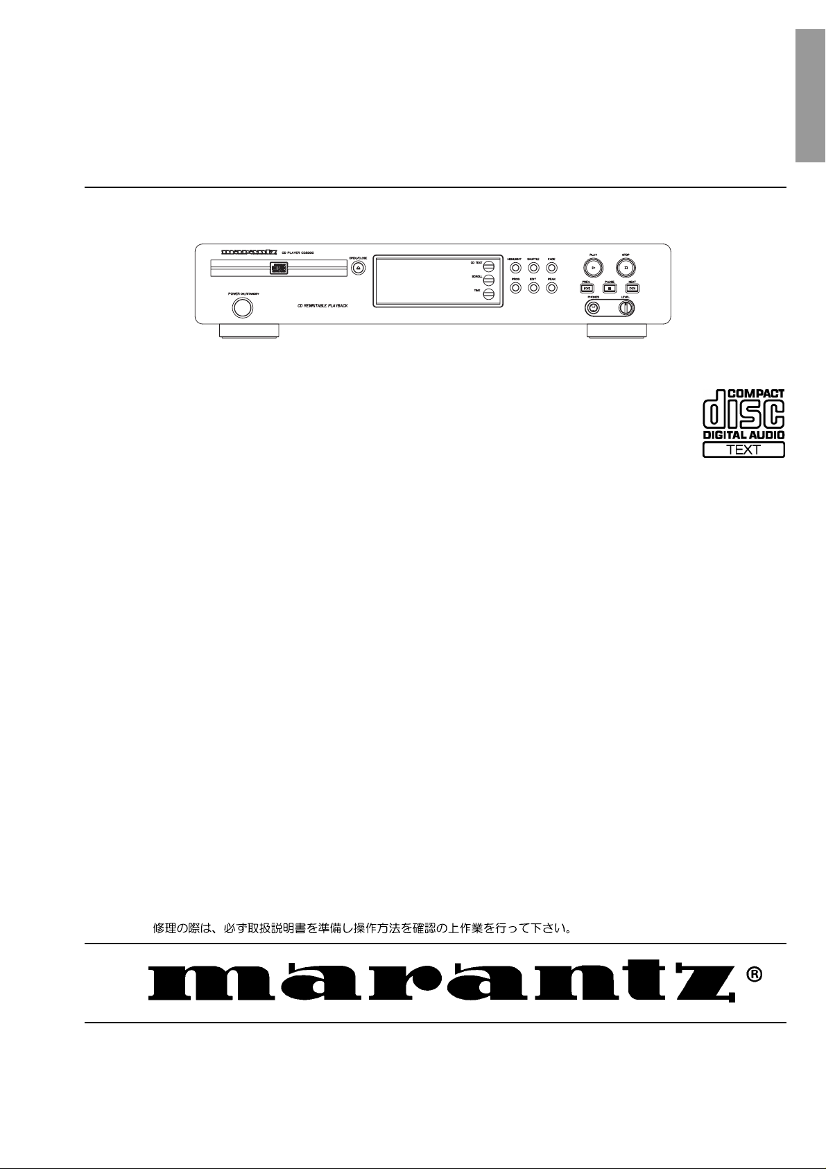
CD5000
Manual
Technical Specification................................................................................................. 2-1
Safety Instructions ....................................................................................................... 3-1
Mechanical Instructions ............................................................................................... 4-1
Service Tools................................................................................................................ 5-1
Service Test Program................................................................................................... 5-2
Blockdiagram ............................................................................................................... 5-3
Wiring Diagram ............................................................................................................ 6-1
Circuit Diagram AF Board/Supply Part......................................................................... 7-1
Component Layout AF Board....................................................................................... 7-2
Circuit Diagram AF Board/DAC Part ............................................................................ 7-3
Component Layout AF Board....................................................................................... 7-4
Circuit Diagram Front Board ........................................................................................ 7-5
Component Layout Front Board................................................................................... 7-6
Circuit Diagram Headphone Board .............................................................................. 7-6
Component Layout Headphone Board ........................................................................ 7-6
Circuit Diagram CD Board ........................................................................................... 7-7
Component Layout CD Board ...................................................................................... 7-8
Fault Finding Tree CD.................................................................................................. 7-9
Exploded View of Set ................................................................................................. 10-1
Exploded View CD Short Loader ............................................................................... 10-2
Electrical Partslist....................................................................................................... 10-3
CD Player
TABLE OF CONTENTS
Please use this service manual with referring to the user guide (D.F.U) without fail.
Printed in Japan
- CD5000 -
273W855010 AO
3120 785 00050
First Issue:1999.06
Page 2
MARANTZ DESIGN AND SERVICE
Using superior design and selected high grade components, MARANTZ company has created the ultimate in stereo sound.
Only original
it is famous.
Parts for your
ORDERING PARTS :
Parts can be ordered either by mail or by Fax.. In both cases, the correct part number has to be specified.
The following information must be supplied to eliminate delays in processing your order :
1. Complete address
2. Complete part numbers and quantities required
3. Description of parts
4. Model number for which part is required
5. Way of shipment
6. Signature : any order form or Fax. must be signed, otherwise such part order will be considered as null and void.
MARANTZ parts can insure that your MARANTZ product will continue to perform to the specifications for which
MARANTZ equipment are generally available to our National Marantz Subsidiary or Agent.
USA
MARANTZ AMERICA, INCMARANTZ AMERICA, INC.
440 MEDINAH ROAD
ROSELLE, ILLINOIS 60172
USA
PHONE : 630 - 307 - 3100
FAX : 630 - 307 - 2687
SUPERSCOPE TECHNOLOGIES, INC.SUPERSCOPE TECHNOLOGIES, INC.
MARANTZ PROFESSIONAL PRODUCTS
2640 WHITE OAK CIRCLE, SUITE A
AURORA, ILLINOIS 60504 USA
PHONE : 630 - 820 - 4800
FAX : 630 - 820 - 8103
AMERICAS
AUSTRALIA
SCAN AUDIO PTY. LTD.SCAN AUDIO PTY. LTD.
52 CROWN STREET, RICHMOND 3121
VICTORIA
AUSTRALIA
PHONE : +61 - 3 - 9429 - 2199
FAX : +61 - 3 - 9429 - 9309
NEW ZEALAND
SCAN AUDIO PTY. LTD.SCAN AUDIO PTY. LTD.
8C PIERMARK DRIVE, ALBANY.
NORTH SHORE, AUCKLAND.
NEW ZEALAND
PHONE : +64 - 9444 - 4710
FAX : +64 - 9444 - 1346
EUROPE / TRADING EUROPE / TRADING
MARANTZ EUROPE B.V.MARANTZ EUROPE B.V.
P.O.BOX 80002, BUILDING SFF2
5600 JB EINDHOVEN
THE NETHERLANDS
PHONE : +31 - 40 - 2732241
FAX : +31 - 40 - 2735578
CANADA
LENBROOK INDUSTRIES LIMITEDLENBROOK INDUSTRIES LIMITED
633 GRANITE COURT,
PICKERING, ONTARIO L1W 3K1
CANADA
PHONE : 905 - 831 - 6333
FAX : 905 - 831 - 6936
THAILAND
MRZ STANDARD CO.,LTDMRZ STANDARD CO.,LTD
746 - 754 MAHACHAI ROAD.,
WANGBURAPAPIROM, PHRANAKORN,
BANGKOK, 10200 THAILAND
PHONE : +66 - 2 - 222 9181
FAX : +66 - 2 - 224 6795
TAIWAN
PAI- YUING CO., LTD.PAI- YUING CO., LTD.
6 TH FL NO, 148 SUNG KIANG ROAD,
TAIPEI, 10429, TAIWAN R.O.C.
PHONE : +886 - 2 - 25221304
FAX : +886 - 2 - 25630415
BRAZIL
MARANTZ BRAZILMARANTZ BRAZIL
CAIXA POSTAL 21462
CEP 04698-970
SAO PAULO, SP, BRAZIL
PHONE : 0800 - 123123
FAX : +55 11 534. 8988
(Discagem Direta Gratuita)
SINGAPORE
WO KEE HONG (S) PTE LTDWO KEE HONG (S) PTE LTD
WO KEE HONG CENTRE
NO.23, LORONG 8, TOA PAYOH
SINGAPORE 319257
PHONE : +65 2544555
FAX : +65 2502213
MALAYSIA
WO KEE HONG ELECTRONICS SDN. BHD.WO KEE HONG ELECTRONICS SDN. BHD.
NO. 102 JALAN SS 21/35, DAMANSARA
UTAMA, 47400 PETALING JAYA
SELANGOR DARUL EHSAN, MALAYSIA
PHONE : +60 3 - 7184666
FAX : +60 3 - 7173828
JAPAN
Technical
MARANTZ JAPAN, INC.MARANTZ JAPAN, INC.
35- 1, 7- CHOME, SAGAMIONO
SAGAMIHARA - SHI, KANAGAWA
JAPAN 228-8505
PHONE : +81 42 748 1013
FAX : +81 42 748 9190
KOREA
MK ENTERPRISES LTD.MK ENTERPRISES LTD.
ROOM 604/605, ELECTRO-OFFICETEL, 16-58,
3GA, HANGANG-RO, YONGSAN-KU, SEOUL
KOREA
PHONE : +822 - 3232 - 155
FAX : +822 - 3232 - 154
SHOCK, FIRE HAZARD SERVICE TEST :
CAUTION : After servicing this appliance and prior to returning to customer, measure the resistance between either primary AC
cord connector pins ( with unit NOT connected to AC mains and its Power switch ON ), and the face or Front Panel of product and
controls and chassis bottom.
Any resistance measurement less than 1 Megohms should cause unit to be repaired or corrected before AC power is applied, and
verified before it is return to the user/customer.
Ref. UL Standard No. 1492.
In case of difficulties, do not hesitate to contact the Technical
Department at above mentioned address.
990521A.O
Page 3
2-1
General
Dimensions (WxHxD) : 435 x 86 x 265mm
Weight : 2,9kg
Accessories
Instruction for use : 3139 116 19120 for /F
: 3139 116 19130 for /K
: 3139 116 18900 for /N, /T
: 3139 116 19110 for /U
Remote control : 3139 228 82600
Mains voltage
/N, /T : 220-230V( 10%) 50Hz
/K :110-120/220230V( 10%) 50/60Hz
/U :120V( 10%) 60Hz
/F :100V( 10%) 50/60Hz
Power consumption
stand by : 5W
operating : approx. 8W
Audio performance
Number of channels : 2
Output voltage (Line out) : 2V
RMS
3dB
Unbalance left-right : 1dB
Frequency response : 20Hz-20kHz 0,4dB
Signal to noise ratio : 108 dB typ.
Dynamic range : 105dB typ. at 1kHz
THD : 0,0063% at 1kHz
Channel separation : 98dB typ. at 1kHz
Headphone output
Output level (1kHz, 0dB) : 5V
RMS
Unbalance left-right : 1,2dB
Output impedance : 120
Load impedance : 32 - 600
Output power : 25mW at 32
: 52mW at 120
: 29mW at 600
Laser
Output power : <5mW (3mW typ.)
Wavelength : 780nm
Measurement setup
Use Audio Signal disc SBC429 4822 397 30184
L
R
LEVEL METER
e.g. Sennheiser UPM550
with FF-filter
S/N and distortion meter
e.g. Sound Technology ST1700B
TECHNICAL SPECIFICATION
sdnammoC5CR
02=edocmetsyS
dnammoC edoC dnammoC edoC dnammoC edoC
"0"YEK LLORCSYALPSID15ELFFUHS28
"1"YEK YALP53THGILHGIH43
"2"YEK POTS54TAEPER29
"3"YEK ESUAP48EDAF201
"4"YEK EMIT11PUEMULOV16
"5"YEK SUOIVERP33NWODEMULOV17
"6"YEK WEIVER50YBDNATS12
"7"YEK EUC52TXETDC88
"8"YEK MARGORP36TXEN32
"9"YEK B/ATAEPER59
0
1
2
3
4
5
6
7
8
9
Page 4
3-1
WARNING
All ICs and many other semiconductors are susceptible to
electrostatic discharges (ESD). Careless handling during
repair can reduce life drastically.
When repairing, make sure that you are connected with the
same potential as the mass of the set via a wristband with
resistance. Keep components and tools at this potential.
ATTENTION
Tous les IC et beaucoup d´autres semi-conducteurs sont
sensibles aux décharges statiques (ESD). Leur longévite
pourrait être considérablement écourtée par le fait qu´aucune
précaution nést prise à leur manipulation.
Lors de réparations, s´assurer de bien être relié au même
potentiel que la masse de l´appareil et enfileer le bracelet
serti d´une résistance de sécurité.
Veiller à ce que les composants ainsi que les outils que l´on
utilise soient également à ce potentiel.
WARNUNG
Alle ICs und viele andere Halbleiter sind empfindlich
gegenüber elektrostatischen Entladungen (ESD).
Unsorgfältige Behandlung im Reparaturfall kann die
Lebensdauer drastisch reduzieren.
Sorgen Sie dafür, daß sie im Reparaturfall über ein Pulsarmband mit Widerstand mit dem Massepotential des
Gerätes verbunden sind.
Halten Sie Bauteile und Hilfsmittel ebenfalls auf diesem
Potential.
AVAILABLE ESD PROTECTION EQUIPMENT :
anti-static table mat large 1200x650x1.25mm 4822 466 10953
anti-static wristband 4822 395 10223
connection box (3 press stud connections, 1M ) 4822 320 11307
extendible cable (2m, 2M , to connect wristband to connection box) 4822 320 11305
connecting cable (3m, 2M , to connect table mat to connection box) 4822 320 11306
earth cable (1M , to connect any product to mat or to connection box) 4822 320 11308
KIT ESD3 (combining all 6 prior products - small table mat) 4822 310 10671
wristband tester 4822 344 13999
AVAILABLE JIG for FR980
Extension PCB and wire kit 4822 395 10815
ESD
WAARSCHUWING
Alle IC´s en vele andere halfgeleiders zijn gevoelig voor
electrostatische ontladingen (ESD).
Onzorgvuldig behandelen tijdens reparatie kan de levensduur
drastisch doen vermindern. Zorg ervoor dat u tijdens reparatie
via een polsband met weerstand verbonden bent met hetzelfde
potentiaal als de massa van het apparaat.
Houd componenten en hulpmiddelen ook op ditzelfde potentiaal.
AVVERTIMENTO
Tutti IC e parecchi semi-conduttori sono sensibili alle scariche
statiche (ESD).
La loro longevità potrebbe essere fortemente ridatta in caso di
non osservazione della più grande cauzione alla loro
manipolazione. Durante le riparationi occorre quindi essere
collegato allo stesso potenziale che quello della massa
delápparecchio tramite un braccialetto a resistenza.
Assicurarsi che i componenti e anche gli utensili con quali si
lavora siano anche a questo potenziale.
small 600x650x1.25mm 4822 466 10958
Safety regulations require that the set be restored to its
original condition and that parts which are identical with
those specified be used.
Safety components are marked by the symbol
Les normes de sécurité exigent que l`appareil soit remis
à l`état d`origine et que soient utilisées les pièces de
rechange identiques à celles spécifiées.
Les composants de sécurité sont marqués
DANGER: Invisible laser radiation when open.
AVOID DIRECT EXPOSURE TO BEAM.
Varning !
Advarsel !
Osynlig laserstrålning när apparaten är öppnad och
spärren är urkopplad. Betrakta ej strålen.
Bei jeder Reparatur sind die geltenden Sicherheitsvorschriften zu beachten. Der Originalzustand des Gerätes
darf nicht verändert werden. Für Reparaturen sind Originalersatzteile zu verwenden.
Sicherheitsbauteile sind durch das Symbol markiert.
LASER PRODUCT
Usynlig laserstråling ved åbning når sikkerhedsafbrydere
er ude af funktion. Undgå udsaettelse for stråling.
SAFETY
Veiligheidsbepalingen vereisen, dat het apparaat in zijn
oorspronkeliijke toestand wordt teruggebracht en dat
onderdelen, identiek aan de gespecificeerde, worden toegepast.
De Veiligheidsonderdelen zijn aangeduid met het symbool
Le norme di sicurezza estigono che l´apparecchio venga
rimesso nelle condizioni originali e che siano utilizzati i
pezzi di ricambiago identici a quelli specificati.
Componenty di sicurezza sono marcati con
CLASS 1
Varoitus !
Avatussa laitteessa ja suojalukituksen ohitettaessa olet alttiina
näkymättömälle laserisäteilylle. Älä katso säteeseen !
After servicing and before returning the set to customer
perform a leakage current measurement test from all
exposed metal parts to earth ground, to assure no
shock hazard exists.
The leakage current must not exceed 0.5mA.
CS 53 135
"Pour votre sécurite, ces documents doivent être utilisés par
des spécialistes agréés, seuls habilités à réparer votre
appareil en panne".
Page 5
4-1
CS 53 140
MECHANICAL INSTRUCTIONS
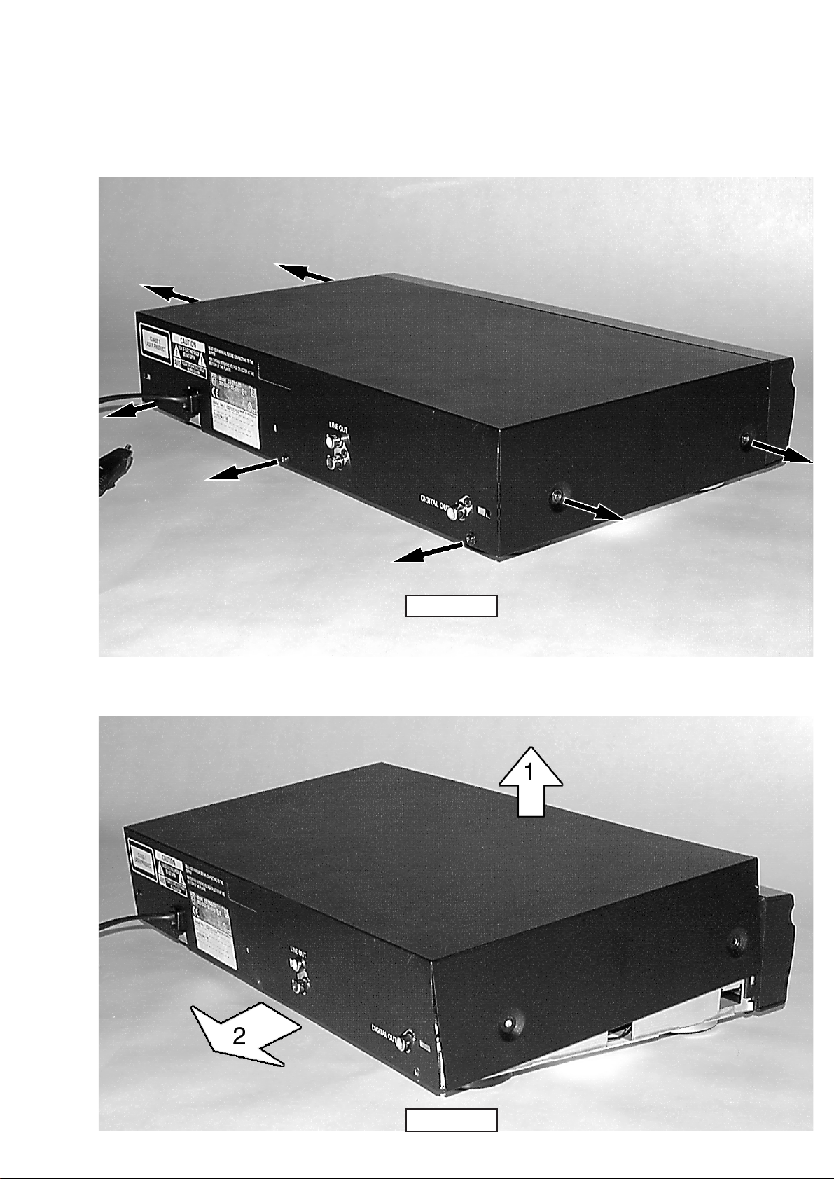
1) Loosen 7x screw as shown in picture 1.
picture 1
picture 2
2) Lift top cover as shown in picture 2.
3) Remove top cover.
Dismantling Top Cover
Page 6
MECHANICAL INSTRUCTION
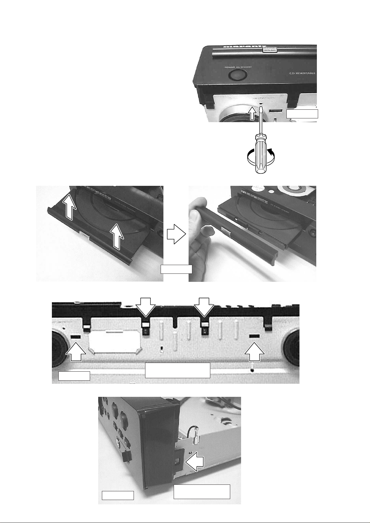
Dismantling Front
1) Press open/close button to open the tray. If the tray doesnít
work, turn counterclockwise a small screwdriver into the
hole as shown in picture 3. Then the tray comes out. After
the first centimeter it is possible to pull the tray out by
hand.
2) Release the door cover of the tray as shown in picture 4.
3) Loosen 2x screw as shown in picture 5.
4) Release 2x snap on button (see picture 5).
5) Release 2x snap on side (see picture 6).
6) Remove front.
4-2
Picture 3
Picture 4
3
3
44
Picture 5
Bottom view
Picture 6
5
Side view
Page 7
4-3
CS 53 142
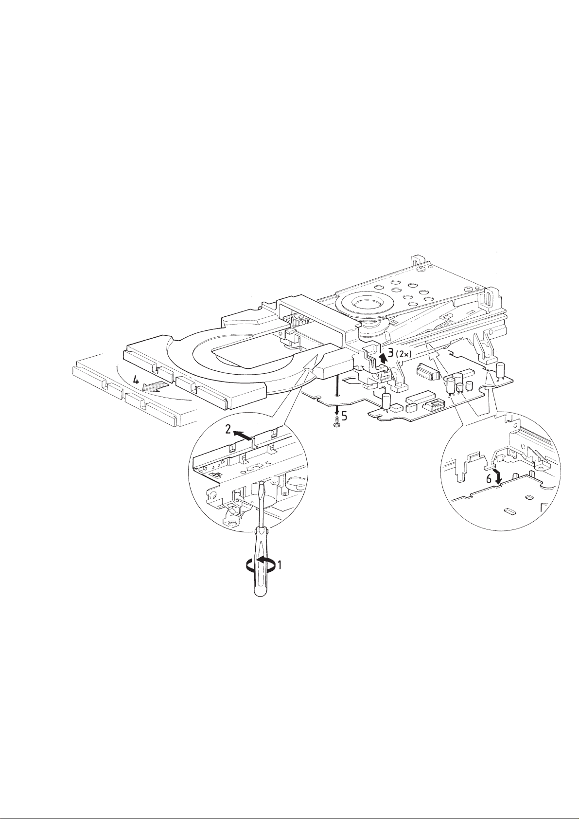
Dismantling hints CD Short Loader
Dismantling the tray
a) Press open/close button to open the tray. If the tray
doesn´t work, use a small screwdriver as shown in Fig.1
step 1 to move the tray outside. After the first centimetre
it is possible to pull the tray out by hand.
b) Release two snaps and remove tray.
Fig. 1
Page 8
4-4
CS 53 143
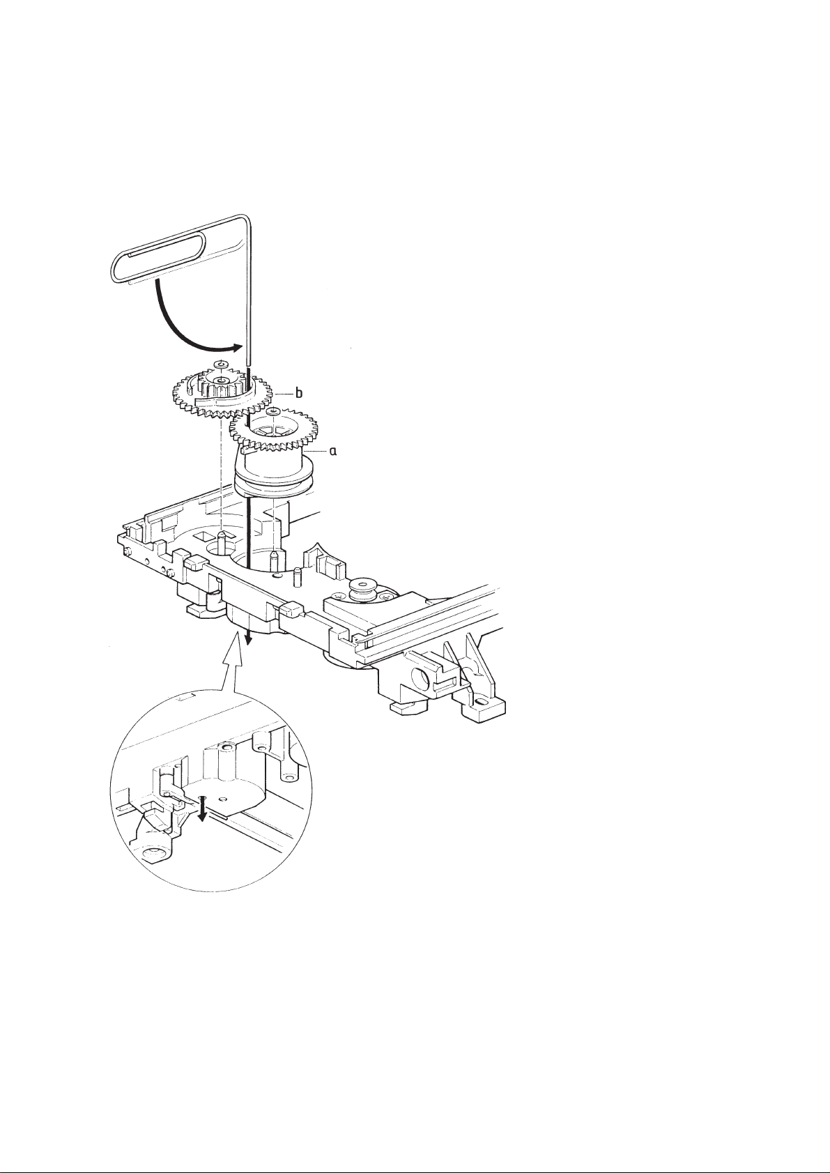
Assembly of gear
a) Use a pin (e.g. a paperclip) to align the cam wheel (a)
with the gear wheel (b). See Fig. 2.
b) Fix the wheels with the small plastic washers.
Fig. 2
Page 9
4-5
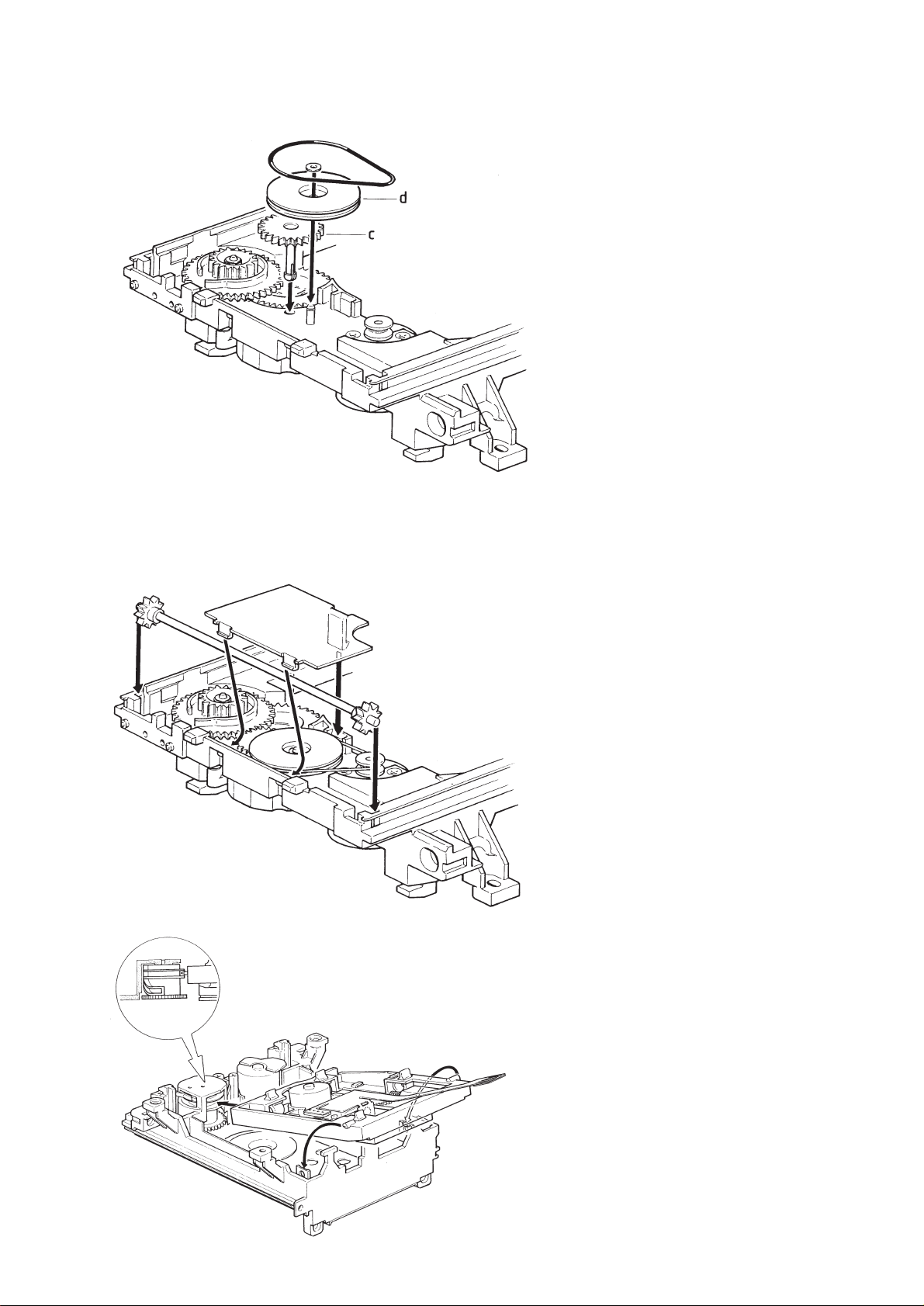
CS 53 144
c) Mount idle wheel 2 (c) and idle wheel 1 (d) in any
position. See Fig. 3.
d) Fix the idle wheel 1 (d) with the small plastic washer.
e) Mount the driving belt.
f) Mount the pinion guiding assy and the cover as shown in
Fig. 4.
g) Turn the gear wheel (b) counter clockwise to
endposition.
Check if tray mechanism works correctly!
1) Turn the gear wheel (b) clockwise to its endposition
(Use a small screwdriver as shown in Fig. 1 step 1).
The tray has to move to inner position first and then the
CD mechanism has to move to its upper position.
2) Turn the gear wheel (b) counter clockwise to its
endposition.
The CD Mechanism has to move to its lower position first
and then the tray has to move outside.
h) Mount the CD Mechanism as shown in Fig. 5.
i) Mount the tray (Align the tray to the chassis and push it
inside).
Fig. 3
Fig. 4
Fig. 5
Page 10

5-1
CS 53 145
HANDLING CHIP COMPONENTS
SERVICE TOOLS
TORX T10 screwdriver with shaftlength 150mm ......................................4822 395 50423
TORX screwdriver set T6 - T20 SBC 163...............................................4822 395 50145
Audio signal disc SBC 429......................................................................4822 397 30184
Playability test disc SBC444/444A..........................................................4822 397 30245
Test disc 444 (disc without errors) +
Test disc 444A (disc with dropout errors, black spots and fingerprints)
Burn in test disc SBC442........................................................................4822 397 30155
(65 min. 1kHz signal at -30dB level without "pause")
Page 11

5-25-2
CS 53 146
N
Y
Y
N
TIME
Button pressed?
YN
TIME
Button pressed?
TIME
Button pressed?
DISPLAY
TEST
DISPLAY TEST
Fig. 1
Fig. 2
Display shows Fig. 1
Display shows Fig. 2
PROGRAM
CD TEXT
PEAK
REPEAT REMTO T AL TRACK TIMESCAN TRACKSHUFFLE 1A-B
1 2 3 4 5 6 7 8 9 10 11 12 13 14 15 16 17 18 19 +
CD TEXT
PEAK
34 7 10131619+
NEXT
Button pressed?
Y
N
FOR CD TEST
see next page
Display becomes dark
Set is in stand by
PLAY
Button pressed?
Y
N
Set works as in normal Mode.
In case of failures error codes
according table 2 will be
displayed.
The CD PLAY Test is intended
to be used for continuously playing
a disc in order to detect intermittend
or not reproducible failures.
The error code indicates where the
failure can be found.
CD
TEST
CD PLAY
TEST
Table 2
CD PLAY TEST
SERVICE TEST PROGRAM
W = Warning
Error number remains on display till next warning/error
F = Fatal error
Set stops playing → Error number remains on display
PROGRAM
Button pressed?
Y
Y
N
N
STOP
Button pressed?
Display shows
8M
Output at
pin80 of 7800=1953,125Hz
QUARTZ
TEST
SHUFFLE
Button pressed?
Y
N
STOP
Button pressed?
Y
N
KEY
TEST
Y
N
any key pressed?
Display shows "--"
Display shows
corresponding key number
(see table 1)
Table 1
KEY TEST
To start service test
program hold
PLAY & STOP depressed
while plugging in
the mains cord
Display shows number of
ROM version
"S Vzz"
S stands for Service Testprogram
V stands for Software Version
zz version number counted from 01 upwards
Service Test Program CD713/CD723 (980429)
yalP3margorP9txeT-DC51
potSTIXEhcraeskaeP01llorcS61
tidE6esuaP21nottubCRynaCR
yeK rebmuN yeK rebmuN yeK rebmuN
txeN1elffuhS7edaF31
suoiverP2nacS8emiT41
esolC/nepO5taepeR11ybdnatS71
rebmunrorrE epyT noitpircseD
0001W
1001W
2001W
3001W
5001W
6001W
7001W
8001W
0201F
rorresucoF
roDCehtpugnitratsnehwemitniatrecanihtiwdnuofebtondluocsucofehtnehwdereggirT
.DCehtgniyalpgnirudemitniatrecaroftsolsisucofehtnehw
rorrelaidaR
.DCehtgniyalpgnirudemitniatrecarofkcartnotonsiovreslaidarehtnehwdereggirT
rorreniedilS
sdnoces6erofeb)desolcsihctiwsrenni(noitisoprennistihcaertondidedilsehtnehwdetareneG
.melborprotomedilsrohctiwsrennI.ybdessapevah
rorretuoedilS
sm052erofeb)neposihctiwsrenni(noitisoprennistifotuoemoctondidedilsehtnehwdetareneG
.melborprotomedilsrohctiwsrennI.ybdessapevah
rorrepmuJ
.emitniatrecanihtiwdnuofebtondluocnoitanitsedpmujehtnehwdetareneG
rorreedocbuS
.emitniatrecarofedocbusdilavoN
rorreLLP
.emitniatrecanihtiwkcoltondluocpooL-kcoL-esahPehT
rorrerotomelbatnruT
.emitniatrecanihtiwpugnitratsgniruddeepsfo%57hcaertondluocDCehtnehwdetareneG
melborprotomcsiD
rorrehcraessucoF
.emitniatrecanihtiwdnuofneebtonsahtniopsucoF
Page 12

5-3 5-3
CS 53 147
NEXT
Button pressed?
Y
N
SHUFFLE
Button pressed?
Y
PROGRAM
Button pressed?
Y
N N
PLAY
Button pressed?
Y
N
NEXT
Button pressed?
Y
PLAY
Button pressed?
N
STOP
Button pressed?
Y
Y
N
PREV
Button pressed?
Y
Display shows
CD
Disc Motor turns CCW
Display shows
CCW
Disc Motor turns CW
Display shows
CW
Slide moves outside
Slide moves inside
Display shows
FOC OK
Display shows
FOC ERR
FOCUS found?
Y
Y
N
STOP
Button pressed?
Y
N
Display shows
FOC XXX
Disc Motor Slide Motor
Focus Servo Test
Motor Test
PLAY
Button pressed?
STOP
Button pressed?
NN
Disc speeds up
Display shows
DISC
Disc Servo Test
PLAY
Button pressed?
Y
Y
STOP
Button pressed?
Y
NN
Display shows
RDL
Radial Servo Test
FOC ERR = Focus not found
FOC OK = Focus found
To start service test
program hold
PLAY & PAUSE depressed
while plugging in
the mains cord
Display shows number of
ROM version
"S Vzz"
In case of focus lost FOC ERR
will be displayed and
Focus Servo Test is entered again
It is possible to control the
slide motor with the
NEXT & PREV button
SERVICE TEST PROGRAM CD-Part
STP-CD Part CD713/CD723 (980429)
Since the CD-RW reflects much less light than an ordinary
CD-A, the gain of the HF-amplifier stage and the sensitivity
of the ADC inside the signal processor must be increased.
The gain is switched via the HG line (pin41 of CD7), the
ADC-sensitivity is switched via software (µP → CD7).
During start-up the correct mode is choosen automatically;
in the service test program it can be switched manually in
order to allow individual measurements in both conditions.
Sensitivity can be toggled
via EDIT Button.
CD RW resp. CD NORM is displayed
for two seconds.
STOP
button pressed in any step returns
to begin of Service Testprogram.
NOTE: If sensitivity is switched to high
the set will not work with normal Audio CDs!
SAA7372 – DECODER AND DIGITAL SERVO IC CD7
Pin Name Direction Description
–––––––––––––––––––––––––––––––––––––––––––––––––––––––––––––––––––––––––––––––––––––––––––––––––––––––––––
1 VSSA1 GND supply (analog) of CD7
2 VDDA1 +4V supply (analog) of CD7
3 D1 HF-preamp → CD7 unipolar current input (central diode signal input)
4 D2 HF-preamp → CD7 unipolar current input (central diode signal input)
5 D3 HF-preamp → CD7 unipolar current input (central diode signal input)
6 VRL GND reference input for ADC
7 D4 HF-preamp → CD7 unipolar current input (central diode signal input)
8 R1 HF-preamp → CD7 unipolar current input (satellite diode signal input)
9 R2 HF-preamp → CD7 unipolar current input (satellite diode signal input)
10 IREFT → CD7 current reference for calibration ADC
11 VRH not connected reference output from ADC
12 VSSA2 GND supply (analog) of CD7
13 SELPLL +4V selects whether internal clock multiplier PLL is used
14 ISLICE CD7 → current feedback from data slicer
15 HFIN → CD7 comparator signal input
16 VSSA3 GND supply (analog) of CD7
17 HFREF → CD7 comparator common mode input
18 IREF → CD7 reference current pin (nom. VDD/2)
19 VDDA2 +4V supply (analog) of CD7
20 TEST1 GND test control input
21 CRIN X-Tal → CD7 crystal/resonator input
22 CDOUT X-Tal → CD7 crystal/resonator output
23 TEST2 GND test control input
24 CL16 not connected 16.9344MHz system clock output
25 CL11 not connected 11.2896MHz or 5.6448MHz clock output (3-state)
26 RA CD7 → servo driver radial actuator output
27 FO CD7 → servo driver focus actuator output
28 SL CD7 → servo driver slide actuator output
29 TEST3 GND test control input
30 VDD1P +4V supply (digital) of CD7
31 DOBM CD7 → digital output bi-phase mark output (3-state)
32 VSS1 GND supply (digital) of CD7
33 MOTO1 CD7 → servo driver motor output1 of CD7; versatile (3-state)
34 MOTO2 CD7 → servo driver motor output2 of CD7; versatile (3-state)
35 SBSY not connected subcode block sync (3-state)
36 SFSY not connected subcode frame sync (3-state)
37 RCK GND subcode clock input
38 SUB not connected P to W subcode bits (3-state)
39 VSS2 GND supply (digital) of CD7
40 V5 not connected versatile output pin of CD7
41 V4 not connected versatile output pin of CD7
42 V3 not connected versatile output pin of CD7 (open drain)
43 KILL CD7 → kill output; programmable (open drain)
44 MISC not connected C2 error flag; output only defined in CD-ROM modes (3-state)
45 DATA CD7 → DAC serial data output (3-state)
46 WCLK CD7 → DAC word clock output (3-state)
47 VDD2P +4V supply (digital) of CD7
48 BCLK CD7 → DAC serial bit clock output (3-state)
49 VSS3 GND supply (digital) of CD7
50 CL4 not connected 4.2336MHz µP clock output
51 SDA µP → CD7 µP interface data I/O line (open drain output)
52 SCL µP → CD7 µP interface clock line
53 RAB µP → CD7 µP interface R/W and load control line
54 SILD µP → CD7 µP interface R/W and load control line
55 NC no connection
56 VSS4 GND supply (digital) of CD7
57 RESET µP → CD7 power-on reset input (active low)
58 STATUS not connected servo interrupt request line/CD7 status register output (open drain)
59 VDD3C +4V supply core (digital)
60 C2FAIL not connected indication of correction failure (open drain)
61 CFLG not connected correction flag output (open drain)
62 V1 → CD7 versatile input pin
63 V2 → CD7 versatile input pin
64 LDON CD7 → 7820 laser drive on output (open drain)
Abbreviations CD Part
Page 13

5-45-4
CS 53 148
BCLK
WCLK
SDA
BCLK
WCLK
SDA
SERIAL DATA
INTERFACE
D/A
D/A
DAC BUFFER
Left out
MUTE
VOLUME
MUTE
Right out
7505
KILL
KILL
STBY
(COMMAND FROM µP)
+5V
Standby circuit
1251
1
2
3
4
5
6
7
1506
1504
1
2
3
4
5
+10V
+5V (switched)
+10V
-10V
+5V
AMPLIFIER
HEADPHONE BOARDAF BOARD
7670
1600
HEADPHONE SOCKET
162
1
2
3
4
5
+10V
-10V
MUTE
LINE OUT
MUTE
1252
1
2
3
4
5
6
7
8
POWERED
KILLI
STBY
STBY
-VKK
F2
F1
+5V
KILLI
(COMMAND FROM µP)
POWERED
KILLP
Mute control
1802
1
2
3
4
5
6
7
BCLK
WCLK
SDA
KILL
+10V
+5V
1250
1
2
3
4
5
6
F1
-VKK
+10V
+5V
-10V
F2
VOLTAGE
SELECTOR
(/01 only)
MAINS PLUG
110V
220V
F1,F2 Filament for FTD (
FRONT BOARD
)
-VKK Supply for FTD (
FRONT BOARD
)
+10V +Supply for buffer and headphone amplifier
-10V -Supply for buffer and headphone amplifier
+5V Stabilized 5V supply for DAC and µP
PROGRAM
CD TEXT
PEAK
REPEA T REMTOT AL TRACK TIMESCAN TRACKSHUFFLE 1A-B
1 2 3 4 5 6 7 8 9 10111213141516171819+
181
1
2
3
4
5
6
7
8
ROM
RAM
VDD
VKK
Converter
A/D
P7
P8
P9
TEST
RESET
DISPLAY-DRIVERS
VSS
CLOCK
P2 P1
P4
P5
P3
P0
P6
8BIT CPU
KEY MATRIX
4
4
IR EYE
7810
+5V
RC5
TRAYTRAY+
TRAY_SW
CD_PORE
CD_DATA
GND
CD_SILD
CD_SICL
µP CLK
GND
SRDT
DOSY
1804
1
2
3
4
5
6
7
8
TRAYTRAY+
TRAY_SW
CD_PORE
CD_DATA
GND
CD_SILD
CD_SICL
182
1
2
3
4
5
6
7
8
POWERED
KILLI
STBY
-VKK
F2
GND
F1
+5V
1810
1
2
3
4
µP CLK
GND
SRDT
DOSY
1720
4
3
2
1
ECO SHORT LOADER
for details see next page
CD753 Blockdiagram 19980604
FRONT BOARD
BLOCKDIAGRAM
Page 14

5-5 5-5
CS 53 149
SAA7372
CD7
TDA1302T
DALAS
R2
D1
D2
D3
D4
R1
BCLK
WCLK
SDA
BCLK
WCLK
SDA
BCLK
WCLK
SDA
HFIN
GAIN SELECTION H=CD-R/W, L=normal CD
R2
D1
D2
D3
D4
R1
LDON
DISC
PHOTO DIODE
ARRAY
TURNTABLE
MOTOR
TRACK
SERVO
FOCUS
SERVO
SLIDE
SERVO
D1 D2
R2R1
D3
FLEX PCB
A/D-CONVERTER
SERIAL
INTERFACE
P
INTERFACE
CONTROL PART
EBU
INTERFACE
RAM
ADDRESS.
SUBCODE
PROCESS.
MOTOR
CONTROL
OUTPUT
STAGES
ERROR
CORRECT.
FRONT END TIMING
DIGITAL PLL
SRAM
EFM
DEMOD.
Vref
KILL
PRE-PROC.
FUNCTION
CONTROL
VERSATILE
INTERFACE
AUDIO
PROCESS.
PEAK
DET.
RA (PWM signal)
RA FO SL
FO
(PWM signal)
SL (PWM signal)
TRACK
FOCUS
DISC Motor-
DISC Motor+
SLIDE Motor+
SLIDE Motor-
FOCUS Servo+
FOCUS Servo-
TRACK Servo+
TRACK Servo-
SLIDE
DISC MOTOR
MOTO1
(from CD7)
MOTO2
(from CD7)
L.P.F.
L.P.F.
L.P.F.
MOTO2MOTO1 16.93MHzDOBM
RESET
1
CD - Drive
VAM1201
pick up
unit
slide motor
t
u
r
n
t
a
b
l
e
Inner switch
TDA7073A
SERVO DRIVER
TDA7073A
MOTOR DRIVER
7851
7802 7819 7860
7852
Laser
on/off
Laser
+5V
ALPC
Automatic Laser Power Control
DATA
RESET
TRAY_SW
TRAY +
TRAY -
SILD
SICL
1802
1804
1803
STABILIZER
+5ESDV
+5V
+4V
+A
+A
+5
7877
TRAY
SUPPLY & AUDIO
INTERFACE
CONTROL INTERFACE
MOTOR
TRAY
7855
TDA7072A
+
-
M
HF-PREAMPLIFIER
CD TEXT (optional)
VDD
SCLK
XMODE
MCK
WFCK
SCOR
SBSQ
EXCK
CD-TEXT INTERFACE
DQSY
SRDT
DQSY
SRDT
uP_CLK
7821
1720
LC89170M
+4V
Timing & Sync
Protection
CRC
Check
CPU
Interface
RAM
32kx8
L.P.F.
L.P.F.
L.P.F.
L.P.F.
L.P.F.
L.P.F.
6
2,5V
0
-2,5V
eye-pattern signal
> 800 mVpp
TB=0.5 s
during focus search
TB=0.1s
2
4
3
5
SDA
WCLK
left channel
MSB
LSB
MSB
right channel
BCLK
TRANSFER OF AUDIO SAMPLES VIA SERIAL INTERFACE OF CD7
CD7 → DAC
1
LSB
ECO SL Mk3 Blockdiagram (IIs) 19980601
BLOCKDIAGRAM ECO SHORTLOADER Mk3
Page 15

6-16-1
blue
red
red
white
green
white
1
1252
1
188
connect cover
1
162
1
184
1
1
182
181
1880
1
1804
1502
1
161
1
1250
1
1251
1
1506
1802
1
1
1
8007
8
8007
8
8006
8
8006
8
8004
8001
connect cover
8010
2
8005
3
8005
3
8001
7
8001
7
8003
5
6
CD MODULE
ECO SL Mk3
FRONT - BOARD
HEADPHONE
STAND BY
AF - BOARD
Digital out
1503
Line out
1504
TRANSFORMER /
TRANSFORMER /K
blue
red
red
white
green
white
Th
ermal fuse
130°C
Thermal fuse
125°C
Mains plug
Mains plug
Voltage selector
black
red 220 - 230V
blue 110 - 127V
WIRING DIAGRAM
1600
GND
DOBM
SHIELD
+10V
-10V
LEFT
AGND
RIGHT
+10V
-10V
LEFT
AGND
RIGHT
KILL
DATA
BCKWS+5V
GND
+10V
POWERED
KILLI
STDBY
-VKKF2F1
GND
+5V
POWERED
KILLI
STDBY
-VKKF2F1
GND
+5V
+A(+10V)
GND
+5V
WS
BCK
DATA
KILL
GND
DOBM
SHIELD
SICL
GND
SILD
DATA
RESET
TRAY_SW
TRAY+
TRAY-
TRAYTRAY+
TRAY_SW
RESET
DATA
SILD
GND
SICL
phones
not for CD713
1810
1
P CLK
GND
SRDT
DOSY
8002
4
1
1720
P CLK
SRDT
DOSY
GND
connect cover
N, /T, /U, /F
/N, /T : 220-230V
/U : 120V
/F : 100V
Page 16

7-1 7-1
6
N, /T, /U, /F
K
1 2 3 4 5 6 7 8
1 2 3 4 5 6 7 8
A
B
C
D
E
A
B
C
D
E
1250 B4
1255 C5
1256 D5
2250 B6
2251 B5
2252 C6
2253 C6
2254 D7
2255 D8
2256 D6
2257 D6
2258 D7
2259 E5
3251 A5
3252 A5
3253 A5
3254 B6
3255 B6
3256 E6
3257 E7
3258 E7
3260 C7
3557 B4
6250 C6
6251 A6
6252 B5
6253 C6
6254 C6
6255 D6
6256 D6
6257 D5
6258 D5
6259 E6
6260 D8
7250 A6
7251 C8
7252 E6
F560 C4
F561 C4
F562 C4
F563 C4
F564 C4
F565 C4
F566 B5
F567 E6
F568 E6
F567
F568
F566
F564
F565
F563
F561
F562
T630mA
1256
F560
T630mA
1255
6R8
3557
1N4003
6260
D2
3260
5R6
2259
220u
22n
2257
4K7
3254
A
POWERED
2K2
3255
470R
3251
470R
3252
F1
+5V
6251
BZX55-C4V7
2
VIN
1
VOUT
3
-VKK
F2
7250
BC327-40
7251
L7805CV
KILLI
KILLP
A
D
A
-10V
A
DD
D2
A
+10V
D2
4K7
3258
3257
4K7
7252
BC558C
1K
3256
BZX79-C3V9
6259
6258
1N4003
2258
1N4003
6257
100n
2255
3m3
2256
22n
2254
4m7
22n
2252
6255
1N4003GP
2253
22n
1N4003GP
6254
1N4003GP
6253
6256
1N4003GP
470n
2250
2251
TO/FROM AF BOARD / DAC PART
220u
BZX79-C27
6250
1N4003
6252
EH-B
1250
/N, /T : 220-230V
/U : 120V
/F : 100V
1
2
3
4
5
6
22K
3253
AF Board / Supply part
5V~
5V~
-28,5V
-31,4V -27,8V -27,8V
10,7V
5,6V
0,6V
-11,7V
3,9V
-8,3V
3,4V
10,2V
9,5V~
9,5V~
V
EVM
...DC voltages measured
in Play mode
Page 17

7-27-2
CS 53 152
AF Board stage .4 19980513
AF Board Componentside view
1250 A1
1251 A4
1252 A1
1255 A1
1256 A1
1502 A4
1503 B4
1504 B1
1505 B4
1506 B1
2250 A1
2251 A2
2252 A1
2253 A1
2254 A2
2255 A3
2256 A1
2257 A1
2258 A2
2259 A2
2501 A3
2502 A3
2503 A4
2504 A3
2505 A4
2506 A4
2507 A3
2508 B3
2511 B2
2512 B2
2513 B2
2514 B1
2515 A3
2516 A4
2521 B2
2522 B3
2523 A3
2524 A4
2527 B4
2540 B4
2541 A4
2543 B4
2544 A4
2545 B4
3251 A1
3252 A1
3253 A1
3254 A2
3255 A1
3256 A2
3257 A2
3258 A2
3260 A3
3500 A3
3501 A2
3502 A4
3503 A4
3504 A4
3505 A3
3506 A3
3507 B2
3508 B2
3509 B3
3510 B3
3511 B2
3512 B2
3513 B2
3514 B2
3515 A3
3527 A2
3532 A2
3533 B4
3534 A3
3535 A3
3537 B2
3538 B3
3539 B2
3540 B1
3541 B2
3542 B2
3543 B1
3544 B2
3545 B1
3547 B1
3548 A2
3550 A4
3552 A4
3553 A4
3556 B4
3557 A1
5801 B4
5803 B4
6250 A1
6251 A1
6252 A1
6253 A1
6254 A2
6255 A1
6256 A1
6257 A2
6258 A1
6259 A2
6260 A3
6500 A2
7250 A1
7251 A3
7252 A2
7500 A3
7501 A2
7504 A2
7505 B2
7507 B1
7508 B1
7509 B1
7510 B1
7511 B4
9253 A1
9254 A2
9256 A2
9257 A2
9258 A2
9262 A3
9263 A3
9264 A3
9265 A3
9266 B3
9267 B1
9269 A2
9270 A3
9272 A4
9274 B4
This assembly drawing shows a summary of all possible versions.
For components used in a specific version
see schematic diagram respectively partslist.
Page 18

7-3 7-3
DRIVER
SOURCES
CURRENT SINKS/
OUTPUT SWITCHES
DATA ENCODERS
NOISE SHAPERS
OVERSAMPLING
TIMING
AND
CONTROL
FILTER
FIR
to headphone
to/from ECO_SL
to/from FRONT
STANDBY
LINE OUT
DIGITAL / OPTICAL OUT
DAC
from ECO_SL
1 2 3 4 5 6 7 8 9 10 11 12 13 14
1 2 3 4 5 6 7 8 9 10 11 12 13 14
A
B
C
D
E
F
G
H
A
B
C
D
E
F
G
H
1251 B1
1252 F14
1502 G2
1503 G4
1504 D14
1505 F7
1506 B14
2501 C4
2502 D4
2503 C4
2504 D4
2505 D7
2506 D5
2507 B8
2508 E7
2511 B10
2512 E10
2513 D13
2514 E13
2515 E4
2516 E4
2521 A9
2522 F9
2523 C2
2524 D7
2527 F6
2540 F2
2541 G3
2543 H4
2544 B2
2545 H3
3500 D2
3501 D2
3502 B3
3503 B3
3504 C3
3505 C4
3506 D4
3507 B8
3508 E8
3509 B8
3510 E8
3511 C9
3512 D9
3513 B10
3514 E10
3515 D4
3527 C10
3532 D10
3533 F5
3534 C10
3535 D2
3537 A8
3538 F8
3539 B12
3540 C12
3541 D12
3542 E12
3543 B12
3544 D12
3545 C12
3547 E12
3548 E3
3550 F4
3552 F4
3553 G4
3556 G4
5801 G3
5803 F6
6500 F11
7500 C2
7501 E2
7502 C7
7504 C10
7505-A E9
7505-B B9
7507 B13
7508 C13
7509 D13
7510 E13
7511-F F4
F510 B1
F511 B1
F512 B1
F513 B1
F514 C1
F515 C1
F516 C1
F517 D2
F518 C4
F519 C5
F520 D5
F521 B8
F522 E7
F523 B8
F524 E7
F525 B14
F526 B14
F527 C14
F528 C14
F529 C14
F530 D14
F531 D14
F532 D14
F540 G2
F541 G2
F542 G2
F543 G4
F544 G4
F545 F7
F546 F7
F550 F14
F551 G14
F552 G14
F553 G14
F554 G14
F555 G14
F556 G14
F557 G14
BC337-40
7510
A
4U7
5803
2545
10n
F523
A
F522
F520
22n
2544
2K2
3527
220R
3537
+10V
220u
2521
A
10n
2523
3538
220R
3514
47K
3532
220K
A
2516
10n
2515
47u
A
+5V
3515
100R
+5V
F546
F545
3552
2K2
22K
3553
F544
F543
F542
F540
F541
13
7
14
12
3556
68R
7511-F
74HCU04N
100n
2543
2540
22u
1
2
34
6
78
GND
2541
5801
PH-B
1502
1
2
3
1u
YKC21-3564
DIGITAL OUT
OPTICAL OUT
preliminary
1503
3
2
1
F531
F532
F530
F556
F557
F555
F553
F554
F551
F552
F550
F528
F529
F526
F527
F525
F524
F521
F519
F517
F518
F516
F514
F515
F512
F513
F511
-10V
+10V
F510
3535
5K6
3533
33R
10K
3548
2K2
NJM4560D
7505-A
3
2
1
4
3534
NJM4560D
7505-B
5
6
7
8
7509
BC337-40
7507
BC337-40
7508
BC337-40
3542
1K
3547
1K
3544
1K
3545
1K
3541
1K
3540
1K
3539
1K
3543
1K
47u
2527
GND
GP1F32T
1505
3
1
2
GND
3503
100R
100R
3504
A
100R
3502
470p
2513
A
A
2K7
3512
3508
4K7
3511
2K7
4K7
3507
+5V
470p
2505
2506
470p
A
47K
3513
A
AA
POWERED
KILLI
STDBY
D
F1
F2
-VKK
+5V
EH-B
1252
1
2
3
4
5
6
7
8
KILL
+5V
-10V
BC557B
7504
KILL
D
3510
4K7
47u
2508
A
4
5
A
2507
47u
EH-B
1506
1
2
3
A
47u
2524
2503
10n
D
4K7
3509
10n
2504
12
2502
47u
DD
D
3506
100R
47u
2501
7501
BC558C
100R
3505
3501
10K
3500
5K6
7500
BC327-40
D
14
VSSD
9
VSSO
1
WS
+10V
STDBY
TDA1549T
2
BCK
16
DATA
5
FILTCL
6
FILTCR
13
NC
3
TEST
11
VDDA
15
VDDD
10
VDDO
4
VOL
7
VOR
8
VREF
12
VSSA
7502
A
+5V
-10V
A
A
A
A
A
A
A
A
A
A
4
3
KILLP
A
A
1N4148
6500
1504
YKC21-3418
1
2
2514
470p
2511
47u
47u
2512
7
220u
2522
EH-B
1251
1
2
3
4
5
6
3550
2K2
WS
SHIELD
DOBM
EBU/GND
KILL
+5
BCK
DATA
AF Board / DAC part
5,4V
-8,3V
-8,3V
-8,3V
-8,3V
5,4V
0V
0V
4,5V
5,1V
5,0V
5,6V
PLAY=5,3V
Stand by=0V
PLAY=1,4V
Stand by=5,5V
PLAY=4,9V
Stand by=5,6V
2,5V
2,5V
0V
0V
0V
0V
-8,3V
-11,2V
0V
0V
0V
0V
11,2V
5V
5V
5V
left channel
MSB
LSB
MSB
LSB
right channel
TRANSFER OF AUDIO SAMPLES VIA SERIAL INTERFACE
TB 0.5 s/Div
4.23MHz
176.4kHz
DATA
WORD SELECT
CLOCK
CLOCK
WORD SELECT
DATA
V
EVM
...DC voltages measured
in Play mode
Page 19

7-47-4
CS 53 154
AF Board stage .4 19980513
AF Board Componentside view
1250 A1
1251 A4
1252 A1
1255 A1
1256 A1
1502 A4
1503 B4
1504 B1
1505 B4
1506 B1
2250 A1
2251 A2
2252 A1
2253 A1
2254 A2
2255 A3
2256 A1
2257 A1
2258 A2
2259 A2
2501 A3
2502 A3
2503 A4
2504 A3
2505 A4
2506 A4
2507 A3
2508 B3
2511 B2
2512 B2
2513 B2
2514 B1
2515 A3
2516 A4
2521 B2
2522 B3
2523 A3
2524 A4
2527 B4
2540 B4
2541 A4
2543 B4
2544 A4
2545 B4
3251 A1
3252 A1
3253 A1
3254 A2
3255 A1
3256 A2
3257 A2
3258 A2
3260 A3
3500 A3
3501 A2
3502 A4
3503 A4
3504 A4
3505 A3
3506 A3
3507 B2
3508 B2
3509 B3
3510 B3
3511 B2
3512 B2
3513 B2
3514 B2
3515 A3
3527 A2
3532 A2
3533 B4
3534 A3
3535 A3
3537 B2
3538 B3
3539 B2
3540 B1
3541 B2
3542 B2
3543 B1
3544 B2
3545 B1
3547 B1
3548 A2
3550 A4
3552 A4
3553 A4
3556 B4
3557 A1
5801 B4
5803 B4
6250 A1
6251 A1
6252 A1
6253 A1
6254 A2
6255 A1
6256 A1
6257 A2
6258 A1
6259 A2
6260 A3
6500 A2
7250 A1
7251 A3
7252 A2
7500 A3
7501 A2
7504 A2
7505 B2
7507 B1
7508 B1
7509 B1
7510 B1
7511 B4
9253 A1
9254 A2
9256 A2
9257 A2
9258 A2
9262 A3
9263 A3
9264 A3
9265 A3
9266 B3
9267 B1
9269 A2
9270 A3
9272 A4
9274 B4
This assembly drawing shows a summary of all possible versions.
For components used in a specific version
see schematic diagram respectively partslist.
Page 20

7-5 7-5
ROM
RAM
VDD
VKK
Converter
A/D
P7
P8
P9
TEST
RESET
DISPLAY-DRIVERS
P4
P5
P1
VSS
CLOCK
P2P3
P0
P6
8BIT CPU
GND
OUT
SUP
V
to/from ECO_SLto/from AF
HLIGHT
SHUFFLE FADE
PRGM
EDIT PEAK
STOP
PLAY
PREV PAUSE NEXT
CD TEXT
OPEN/CLOSE
CD_SICL
CD_SILD
DGND
CD_PORE
TRAY_SW
TRAY+
TRAY-
CD_DATA
TIMESCROLL
preliminary
1 2 3 4 5 6 7 8 9 10 11 12 13
1 2 3 4 5 6 7 8 9 10 11 12 13
A
B
C
D
E
F
G
H
I
A
B
C
D
E
F
G
H
I
181 F1
182 H1
184 E1
1800 C10
1810 I6
1820 F1
1821 F11
1822 F11
1823 F12
1824 F12
1825 F12
1826 F12
1827 F13
1828 G11
1829 G12
1830 F13
1831 G12
1832 G13
1833 H11
1834 H12
1844 G7
2800 B5
2801 B11
2803 I7
2807 I8
2808 G2
2810 I8
2811 G8
2812 E3
2813 H8
2814 E3
2815 D10
3804 H7
3805 H7
3806 H6
3807 H8
3808 H8
3809 I7
3810 E10
3811 E11
3812 E10
3813 F11
3814 F10
3815 F10
3816 F10
3817 F11
3818 G11
3819 G11
3820 H11
3821 G10
3822 E5
3823 F6
3829 E2
3830 E2
3832 F3
3833 F3
3834 F3
3835 F3
3836 E2
3837 G9
3838 H2
3841 H2
3842 H2
3844 G3
3845 G3
3846 G3
3847 D10
3848 B4
3849 B11
5802 E3
6801 D5
6802 D6
6820 I2
7800 D6
7810 H9
7811 H8
9800 G10
1
2
3
4
5
6
7
8
9
182
1N4148
6802
1N4003
6820
3849
4R7
1N4148
6801
3848
10R
F842
F843
F841
D
F840
D
1833 1834
22K
3820
1K
3806
1K
3821
1K
3804
13
P1312P1411P1510P16
9
P223P322P421P520P619P718P817P9
16
1K
3805
30G531G632G733G834G935
NC1
5
NC2
6
NC3
7
NC4
8
NC5
41
P1
24
P1015P1114P12
1800
F111F12
2
F2144F22
45
G1
27
G10
36
G1137G12
38
G13
39
G14
40
G228G329G4
D
14-BT-54GK
FFC
12
34
2803
22n
72
73
74
75
76
77
78
79
8
80
9
1810
58 59660 61 62 63 64
65
66
67
68
69
7
70
71
43 44 45 46 47 48 49550 51 52 53 54 55 56 57
29
3
30
31
32
33
34
35
36
37
38
39
4
40
41 42
14151617181922021222324
25
26
27
28
7800
TMP87CP71F
1
10111213
3847
100R
2815
220n
F823
F826
F825
F824
F821
F800
F814
F815
F812
F813
F811
F809
F810
F808
F801
F816
F803
F802
F804
F806
F805
F807
F818F817
F820
F819
F822
D
D
D
D
1844
CST
D
D
9800
47K
3837
10n
2811
D
D
100n
2813
10n
2810
D
7811
BC547B
5802
2u2
3846
1K
3836
22K
38441K1K
3845
100n
2812
1K
3842
3841
1K
D
1K
3838
3829
22K
2814
47u
1
2
1K
3822
22n
2808
D
184
1K
3816
1K
3814
3815
1K
3818
22K 22K
3817
3823
1K
22K
3819
22K
3830
1820
D
3813
1K
1832
3811
1K
1K
3812
1K
3810
1827
1830
1825
18261824
18311829
1823
10u
2801
2800
10u
D
D
1K
3807
D
DD
3833
1K
1K
3832
38341K1K
3835
DIPMATE
DIPMATE
181
1
2
3
4
5
6
7
8
D
2807
100u
47R
3808
100K
3809
1822
1828
1821
+5V
+5V
7810
1
2
34
+5V
+5V
+5V
+5V
VC
POWERED
KILLI
STDBY
POWERED
KILLI
STDBY
+5V
+5V
+5V
-VKK
VC
G04
G03
+5V
F2
F1
-VKK
F2
F1
VC
VC
P05
P04
P03
P02
P01
G10
G11
G12
G13
G14
P16
P15
P14
P13
P12
P11
P10
P09
P08
P07
P06
G02
G01
G01
G02
G03
G04
G05
G06
G07
G08
G09
G12
G11
G10
G09
G08
G07
G06
G05
G04
G03
P13
P12
P11
P10
P09
P08
P07
P06
P01
G14
G13
P02
P03
P05
P04
P16
P15
P14
FRONT BOARD
CD753 Front Board 19980512
4,9V
-18V
4,8V
4,8V
4,8V
0V
STAND BY
1840
188
GND
Page 21

7-6 7-6 7-6
CD753 Front Board stage .4 19980520
Front Board Componentside view
Front Board Copperside view
181 B1
182 B2
184 B3
1800 A3
1810 B1
1820 A1
1821 A5
1822 B5
1823 A5
1824 B5
1825 A6
1826 B6
1827 A7
1828 B7
1829 B7
1830 A8
1831 B8
1832 A4
1833 A4
1834 B4
1844 B4
2800 A1
2801 A4
2803 B1
2807 B2
2808 B1
2810 B5
2811 B4
2812 B3
2813 B4
2814 B3
2815 A3
3804 B4
3805 B4
3806 B3
3807 B4
3808 B2
3809 B5
3810 A5
3811 A5
3812 A5
3813 B5
3814 B5
3815 B5
3816 B5
3817 B5
3818 B5
3819 B5
3820 B4
3821 A4
3822 B3
3823 B2
3829 B4
3830 B2
3832 B1
3833 B1
3834 B1
3835 B1
3836 B2
3837 B4
3838 B1
3841 B1
3842 B2
3844 B1
3845 B1
3846 B1
3847 B2
3848 A1
3849 A3
5802 B3
6801 A2
6802 A2
6820 B2
7810 B3
7811 B5
9800 B4
9801 A3
9802 A3
9803 A5
9804 A4
9805 A5
9806 A6
9807 A6
9808 A7
9809 A7
9810 B2
9811 B2
9812 B2
9813 B2
9814 B4
9815 B3
9816 B4
9817 B4
9818 B5
9819 B1
9820 A1
7800 B3
7800
7800
Left
Right
AGND
-10V
+10V
6.3mm
*
*
*
*
1 2 3 4
1 2 3 4
A
B
C
A
B
C
F607
220u
2602
F608
F606
F604
F605
F602
F603
F601
3609
10R
3608
3604
120R
15K
3607
120R
3605
3603
15K
3602
10K
10K
161
1
2
10K
3601
DIPMATE
162
1
2
3
4
5
2601
220u
10R
3611
HLJ1540
1600
1
2
3
2610
100n
2603
22n
2604
1n
2605
1n
7670-A
NJM4560D
3
2
1
8
4
3606
10K
7670-B
NJM4560D
5
6
7
8
4
VCC
VSS
VCC
VSS
VCC
VSS
+10V
-10V
+10V
-10V
Headphone Board
10,8V
10,8V
-11,7V
0V
0V
0V
0V
0V
0V
-11,7V
* preliminary
3600-B
10K
10K
3600-A
3600-A B1
3600-B B1
161 C4
162 B1
1600 B4
2601 A3
2602 C3
2603 A2
2604 B3
2605 B3
2610 C4
3601 C2
3602 B2
3603 B3
3604 B3
3605 B2
3606 B2
3607 B3
3608 B3
3609 C3
3611 A4
7670-A C3
7670-B A3
CD753 Headphone Board 1998 05 11
Headphone Board Copperside view
161 B4
162 B2
1600 D2
2601 B2
2602 C3
2603 B3
2604 D3
2605 D1
2610 B4
3600 D4
3601 B4
3602 B4
3603 C2
3604 B2
3605 D2
3606 D3
3607 B3
3608 C1
3609 B3
3611 B1
7670 B3
9600 C4
9601 C4
9602 C4
9603 C4
9604 D4
This assembly drawing shows a summary of all possible versions.
For components used in a specific version
see schematic diagram respectively partslist.
Page 22

7-7 7-7 7-7
LS
Vdd
O4
O6
O3
O1
O5
O2I2
I5
I1
I3
I6
I4
DALAS
Vg
Vdd
LDon
MI
Lo
Adj
C
GNDL
Vrfe
Vrf
HG
CD TEXT
PDM
for coax out: 3875 = 22R
22p
for COAXIAL OUT version only
not for flap
comm.cath
D1
D5
D3
D2
D4
INNERSWITCH
-
+
-
+
-
-
+
+
CD DRIVE
VAM 1201
Track
Focus
MM
SLEDGE
DISC
Do not split cables!
length 30cm
for OPTICAL OUT version only
during speed up play brake
Timing & Sync
Protection
CRC
Check
CPU
Inter-
face
32kx8
RAM
M
TRAY
MOTOR
Loader
for TRAY Version only
for FLAP version only
##
(H = CD-R/W)
(H = Laser On)
CD R/W Front End
WS
SDA
BCLK
TRAY_SW
SICL
SICL
SILD
SILD
RESET
RESET
DATA
DATA
SWITCH
INNERSWITCH
INNERSWITCH
#
NFR: +A = 8 ... 13.5V
PTC: +A = 6 ... 13.5V(only for battery powered versions)
JST EH
TRAY
Break-Away PB OPT OUT
VDD
DQSY
SRDT
SCLK
SW2
SW1
TEST
GND
XMODE
MCK
WFCK
SCOR
SBSQ
EXCK
CD-TEXT INTERFACE
only if not CD-TEXT
TURNTABLE
TRAY_SW
TRAY-
TRAY+
KILL
SUPPLY & AUDIO INTERFACE
CONTROL INTERFACE
WS
SDA
HF
SLIDE
BCLK
+5V
GND
+A
FOCUS
TRACK
SERVO-DRIVER
MOTOR-DRIVER
RESET
DATA
SILD
KILL
SICL
GND
JST PH
for BLER measurement
CFLG output (open drain)
"L"=dig out, "H"= no dig out
EBU_GND
SHIELD
DOBM
+5V
DOBM (TTL)
GROUND
for Coaxial: for Optical:
JST PH
resistor for flap version only
SHARP TOSLINK
JST EH
1
2
3
4
5
6
JST EH
DQSY
SRDT
uP_CLK
JST FE hor
JST PH
(to versatile pin 63 of decoder IC)
#
#
[7]
1
2
3
4
5
6
7
8
for R/W: 270k
for coax. out: 33R
#
##
#
#
#
[1]
[2]
[3]
[4]
[5]
[6]
[6]
[5]
[4]
[3]
[2]
[1]
# ... for provision only
CD-BOARD
(
ECO-SL Mk3)
3245671 8 9 10 11 12 13 14 15 16 17 18 192 20 21 22 23 24 25 26 27 28 293 30 31
L
K
J
O
I
H
G
F
E
D
C
B
A
N
M
L
K
J
O
I
H
G
F
E
D
C
B
A
N
M
3245671 8 9 10 11 12 13 14 15 16 17 18 192 20 21 22 23 24 25 26 27 28 293 30 31
HF HF HF HF HF
HF
L
L
L
DA
L
L
L
L
L L
L
+5ESD
+5ESD
+4V
+5ESD
SVDDA1
T730
100n
2802
18p
2810
47n
2809
47n
2870
47n
2831
100n
2898
2848
10n
560p
2820
1n5
2823
2n2
2814
15k
3806
33k
3804
10k
3803
3883
100
3858
100
3818
120k
3817
4k7
560
3807
4k7
3882
10k
3827
10k
3828
10k
3829
10k
3830
10k
3825
3826
10k
PC74HCU04D
7819
F
13 12
1
PC74HCU04D
7819
E
11 10
1
PC74HCU04D
7819
D
98
1
PC74HCU04D
7819
C
56
1
PC74HCU04D
7819
B
34
1
PC74HCU04D
7819
A
12
1
2899
4u7
BC337/40
7822
7802TDA1302T
16
15
14
13 12
11
10
9
8
7
6
5
4
3
2
1
24
23
22
21
20
19
18
17
D
D
D D
D
L HF
DA
D
D
HF
HF
HF
DA
L
D
D
EBU
D EBU
D
D
D
D
DD
D
D
D
D
D
D
EBUEBUEBU
L
DA
to 3881
from 7860/Pin 41
TRAY_SW
TRAY+TRAY-
TRAY_SW
TRAY+
TRAY-
R2
R1
D4
D3
D2
D1
VDDA1
+A_TRAY +A_TRAY
+4V
+5ESD
+4V
+4V
+4V
+4V
+A
+5ESD
+4V
+5V+A+A
+4V +5V
+4V
+A_TRAY
+4V
+4V
+4V
+5V
DD4
DD5
DD3
DD2
DD1
LD-
HF
V4
LD_ON
47n
2722
1u/16V
2865
100n
2869
47p
2845
2861
22p
2862
22p
2856
47n
2857
22n
2858
47p
100n
2853
2851
10n
220p
2830
220p
2829
220p
2828
220p
2827
10n
2839
5n6
2836
2825
220p
2826
220p
2837
560p
2840
1n8
100n
2819
10n
2761
2890
10n
2842
2868
47p
100n
2838
1n
2720
47p
2721
10n
2891
100n
2818
100k
3857
33k
3895
1k8
3893
33k
3892
1k
3891
1k
3890
470
3721
22
3898
100
3875
3879
560
10k
3842
3763
3764
220R
220R
220R
3762
100
3860
100
3861
33
3832
1M
3862
22k
3856
1k
3844
3872
100
1k
3852
27k
3851
3853
6k8
1k
3820
1k2
3839
1k2
3836
39k
3843
22k
3838
27k
3835
1k
3815
3837
6k8
3840
6k8
3874
10k
3873
10k
3870
10k
3876
180
10
3871
100
3864
3896
330
470
3897
39k
3845
1k
3846
220
3751
3752
220
220
3865
10k
3867
10k
3866
10k
3868
10k
3869
220
3863
3848
1k
3850
1k
1k
3833
220
3859
10k
3819
3753
220
10k
3880
390k
3854
4k7
3881
47
3729
10k
3728
470
3727
470
3726
470
3725
470
3720
470
3723
470
3722
470
3724
10
3899
10
3894
4k7
3730
47u
2859
4u7/16V
2860
2847
47u/16V
2843
0.47u
2849
47u/16V
47u/16V
2863
4u7/16V
2844
2850
4u7
1u
2892
BC547C
7878
BC547B
7877
7821 LC89170M
10
11
12
13
141
2
3
4
5
6
7
8
9
1895
YKC21
1804
1890
1
2
3
1880
1
2
3
1881
1
2
3
9802
9800
9801
9803
9890
5890
920927-152B
1
2
34
6
MT
1807
1
2
1803
1
2
1850
1
2
1820
Leaf Switch
1810
2
17
1
100u AL04
5802
10u AL02
5810
1u AL02
5804
6888
BZX79F2V4
7855
TDA7072A
6
1
2
3
8
5
input-
input+
GND
+Vp
out-
out+
1720
1
2
3
4
9804
1802
7896
1
2
3
GP1F32T
IC
Driver
3R3
3849
3841
3R3
8.46MHz
5860
SAA7378
7860
10
11
12
13
14
15
16
17 18 19120 21 22 23 24 25 26 27 28 29230 31 32
33
34
35
36
37
38
39
3
40
41
42
43
44
45
46
47
48
4945051525354555657585956061626364
6
7
8
9
PINS
MICROPROCESSOR
V1...VV5
INTERFACE
DETECT
PEAK
KILL
MOTO2
MOTO1
WCLK
VDD2P
SCLK
SBSY
SFSY
VSS2
MISC
DATA
RCK
SUB
KILL
V5
V4
V3
VSSA1
VSSA3
SELPLL
HFIN
Vref
D3
D2
D1
VSSA2
VRH
IREFT
R2
R1
D4
VRL
VDDA1
ISLICE
DIGITAL
DEMOD.
CORRECTION
ERROR
PROC.
PRE-
EFM
PLL
CONTROL PART
CONTROL
FUNCTION
SRAM
FLAGS
TIMING
CONTROL
MOTOR
INT.
EBU
ADDR.
RAM
VERSATILE
OUTPUT
STAGES
FO
SILD
SL
RAB
TEST3
SCL
SERIAL DATAAUDIO
VDD1P
LDON
INTERFACEPROCESSOR
SDA
DOBM SUBCODE
CL4PROCESSOR
VSS1
VSS3
ADC
IREF
FRONT END
V2
VDDA2V1TEST1
CFLG
CRIN
C2FAIL
CROUT
VDD3C
TEST2
STATUS
CL16
RESET
CL11
HFREF
VSS4
RA
NC
1806
1
2
3
4
5
6
1801
10
11
12
1
2
3
4
5
6
7
8
9
PTC 4R6
3847
TDA7073A
7851
14
10
1
2
6
7
11
3
4
13
16
9
12
5
8
15
+
-
VDD
+
-
TDA7073A
7852
14
10
1
2
6
7
11
3
4
13
16
9
12
5
8
15
+
-
VDD
+
-
2767
2765
22p
22p
22p
2764
470p
2766
SUPPLY FOR 7819
470
3771
HF PRE-AMPLIFIER
TO 1804
FROM 1810
0V
4V
0V 0V
4V
0V 0V
0V
4V
1720J32
1801G2
1802F32
1803G26
1804D21
1806M2
1807H31
1810H30
1820H32
1850C16
1880M23
1881M27
1890M30
1895M29
2720L27
2721L27
2722I30
2761F28
2764E24
2765E24
2766C26
2767E25
2802C10
2809D8
2810D9
2814D11
2818J3
2819J4
2820I9
2823I9
2825I11
2826I11
2827I11
2828I12
2829I12
2830I12
2831G7
2836K10
2837K9
2838E20
2839L10
2840L9
2842E17
2843N9
2844F14
2845E19
2847J9
2848F5
2849M9
2850N14
2851N9
2853N10
2856K14
2857L15
2858K14
2859M31
2860L15
2861L17
2862L16
2863E17
2865H26
2868D19
2869K19
2870G4
2890N21
2891N29
2892M28
2898I4
2899G4
3720I27
3721J27
3722J27
3723K27
3724K27
3725J30
3726J30
3727K30
3728J31
3729I31
3730I29
3751E19
3752E19
3753E18
3762F22
3763F22
3764G22
3771C26
3803D9
3804C10
3806D9
3807C11
3815D12
3817G4
3818F5
3819D15
3820J3
3825H10
3826H10
3827G10
3828G10
3829G10
3830G10
3832E14
3833K16
3835K10
3836K10
3837K9
3838L10
3839L10
3840L9
3841J10
3842E15
3843N10
3844O9
3845O10
3846O9
3847J10
3848M14
3849M10
3850N14
3851M10
3852N10
3853M9
3854I14
3856J14
3857K15
3858E7
3859E16
3860K17
3861L16
3862K16
3863E17
3864F21
3865E18
3866A18
3867A18
3868A18
3869A18
3870D19
3871E16
3872C20
3873A19
3874A20
3875L19
3876F28
3879F27
3880B22
3881F11
3882E8
3883G3
3890H29
3891G29
3892G29
3893G29
3894M22
3895G28
3896M22
3897N22
3898M31
3899M29
5802G27
5804E26
5810E29
5860L16
5890M28
6888H30
7802E7
7819C3
7819C4
7819C5
7819C6
7819C7
7819D10
7821I28
7822I5
7851J8
7852M8
7855G28
7860F15
7877E28
7878C19
7896M32
9800C19
9801D15
9802G27
9803E28
9804J20
9890N22
2V
2V4V2V2V2V1.8V1.8V
0V
4V
0V
2V
4V
0V
4.2V 5.6V
4.9V
4.8V
4.8V
10V
2.4V
2.4V
5.6V
10V
V
EVM
...DC voltages measured
in Play mode
4V
2.7V
0V
1.3V
1 SEC
0.7V
4.6V
3.8V
4V
0V
LASER
ON/OFF
6
during focus search
5.4V
0.4V
1V
5.4V
10V
10V
2V
2V
10V
2V
2V
2V
2V
0.5V
0.3V
1.3V1.3V
eye-pattern
1
PDM
3
4 2
TB=0,5 us/DIV
3.8V
1.8V1.7V
11.29MHz
4.1V
0.8V
4.2V
2V
2V
5
4V 0V 4V 4V 3.3V0V0.2V 3.3V
4V2V2V
0V
4V
0V 0V
0V 0V
Page 23

7-8 7-8 7-8
3103 303 3397.2
ECO SL Mk3 (R/W&IIs) Layout stage .2 (19980330)
F
E
D
C
B
A
F
E
D
C
B
A
654321
654321
DISC MOTOR CONNECTION
(break away part)
ECO Short Loader Mk3
Copperside view
BC...
12
1
1850
9841
1
3876
7877
9800
3879
2761
9803
5810
7878
2847
FOIL
8820
FOCUS & TRACK
SERVO DRIVER
SCREENING
1804
3874
2868
9806
9816
9810
9820
5804
9801
3873
3871
3872
3870
3854
3859
3865
3866
3867
3868
3869
2856
2863
3752
3753
3819
38323842
3863
2825
28262827
2828
2829
2830
2842
2844
2818
2819
3815
3820
3856
9811
9825
1
9
1
9807
9809
9814
3853
7851
7852
3837
3839
3841
3847
3849
3852
2837
2840
2849
2851
3836
3840
1
1880
3880
3894
9817
9890
1
9804
9821
9840
3881
3896
3897
5860
3724
3751
3860
3864
3875
3763
3762
3764
2838
2845
2858
2869
2890
3721
3722
3723
3838
9823
3845
3848
3850
3851
3857
3862
3861
3720
3833
3835
3843
2862
2861
2860
2857
2721
1801
2836
2839
2853
6
9815
9819
9822
9824
98309839
9831
3728
3729
3844
3846
SLIDE & DISC
MOTOR DRIVER
3730
1806
2843
2850
3725
3726
3727
2722
2720
9
1802
9892
1
1810
9808
9842
9805
1
1
8
1
12
1807
TRAY MOTOR
DRIVER
7855
9802
3892
3893
3895
5802
1720
3890
3891
6888
2814
2802
2810
3803
3804
7822
3807
3882
9851
3806
3817
3818
3827
3828
3829
3830
3858
3883
2809
2831
2848
2870
2898
2820
2823
2899
3825
3826
9847 9850
3771
9703
9704
2764
2765
2766
2767
9705
9701
9702
5
2
3
4
1 6
SICL
GND
GND
DOBM
+5V/SHIELD
SILD
DATA
RESET
TRAY MOTOR+
-
TRAY_SW
+A
GND
+5V
WS
BCLK
SDA
KILL
P CLK
GND
SRDT
INNERSWITCH
GND
DISC+
DISCSLIDE+
SLIDE-
DQSY
HF-AMPLIFIER
HF PRE-AMPLIFIER
DALAS
SIGNAL PROCESSOR
CD-TEXT
7819
7802
7860
7821
2865
3103 303 3397.2
654321
DISC MOTOR CONNECTION
(break away part)
BC...
This assembly drawing shows a summary
of all possible versions.
For components used in a specific version
see schematic diagram respectively partslist.
ECO SL Mk3 (R/W&IIs) Layout stage .2 (19980330)
F
E
D
C
B
A
F
E
D
C
B
A
654321
HF-AMPLIFIER
SIGNAL
PROCESSOR
7819
7802
7860
2865
CD-TEXT
12
1
1850
9841
1
3876
7877
9800
3879
2761
9803
5810
7878
2847
FOIL
8820
FOCUS & TRACK
SERVO DRIVER
SLIDE & DISC
MOTOR DRIVER
SCREENING
1804
3874
2868
9806
9816
9810
9820
5804
9801
3873
3871
3872
3870
3854
3859
3865
3866
3867
3868
3869
2856
2863
3752
3753
3819
38323842
3863
2825
2826 2827
2828
2829
2830
2842
2844
2818
2819
3815
3820
3856
9811
9825
1
9
1
9807
9809
9814
3853
7851
7852
3837
3839
3841
3847
3849
3852
2837
2840
2849
2851
3836
3840
1
1880
3880
3894
9817
9890
1
9804
9821
9840
3881
3896
3897
5860
3724
3751
3860
3864
3875
3763
3762
3764
2838
2845
2858
2869
2890
3721
3722
3723
3838
9823
3845
3848
3850
3851
3857
3862
3861
3720
3833
3835
3843
2862
2861
2860
2857
2721
1801
2836
2839
2853
CD-TEXT
6
9815
9819
9822
9824
98309839
9831
3728
3729
3844
3846
3730
1806
2843
2850
3725
3726
3727
2722
2720
9
1802
9892
1
1810
9808
9842
9805
1
1
8
1
12
1807
TRAY MOTOR DRIVER
7855
9802
3892
3893
3895
5802
1720
3890
3891
6888
2814
2802
2810
3803
3804
7822
3807
3882
9851
3806
3817
3818
3827
3828
3829
3830
3858
3883
2809
2831
2848
2870
2898
HF-AMPLIFIER
2820
2823
2899
3825
3826
9847 9850
3771
9703
9704
2764
2765
2766
2767
9705
9701
9702
Componentside view
5
2
3
4
1
6
SICL
GND
GND
DOBM
+A
GND
+5V
WS
BCLK
SDA
KILL
+5V/SHIELD
SILD
DATA
RESET
TRAY MOTOR+
-
TRAY_SW
P CLK
GND
SRDT
GND
DISC+
DISC-
SLIDE+
SLIDE-
DQSY
INNERSWITCH
1720 C1
1881 opt.
1890 opt.
1895 opt.
17 opt.
1801 D3
1802 C6
1804 E6
1806 C1
1807 B2
1810 B5
1820 B3
1850 F6
1880 D6
2720 C3
2721 C3
2722 C2
2761 F5
2764 B5
2765 B5
2766 B5
2767 B5
2802 F4
2809 E4
2810 F3
2814 F4
2818 F3
2819 F3
2820 D4
2823 D4
2825 E4
2826 E4
2827 E4
2828 F5
2829 F5
2830 F5
2831 E3
2836 D3
2837 E2
2838 D5
2839 D3
2840 F2
2842 E5
2843 D2
2844 E5
2845 D5
2847 F1
2848 E3
2849 E1
2850 D2
2851 E2
2853 D3
2856 E4
2857 D4
2858 D4
2860 D4
2859 opt.
2891 opt.
2892 opt.
2865 A1
2861 D4
2862 D4
2863 E5
2868 F5
2869 D5
2870 E3
2890 D5
2898 F3
2899 D3
3720 C3
3721 C5
3722 C5
3723 C5
3724 C4
3725 C2
3726 C2
3727 C2
3728 C2
3729 C2
3730 C2
3751 D5
3752 E5
3753 E5
3762 D5
3763 D6
3764 D5
3771 D5
3803 F4
3804 F4
3806 F4
3807 F4
3815 E4
3817 E3
3818 E3
3819 E5
3820 F3
3825 D4
3826 D4
3827 E4
3828 E4
3829 E4
3830 E4
3832 E5
3833 D4
3835 D3
3836 E2
3837 E2
3838 C3
3839 E2
3840 F2
3841 E2
3842 E5
3843 C4
3844 D2
3845 C4
3846 D2
3847 E2
3848 D3
3849 E2
3850 D3
3851 C3
3852 E2
3853 E2
3854 E4
3856 E4
3857 D4
3858 E3
3859 E5
3860 D4
3861 D4
3862 D4
3863 E5
3864 D5
3865 E5
3866 E5
3867 E5
3868 E5
3869 E5
3870 F5
3871 E5
3872 F5
3873 F5
3874 F6
3875 C5
3876 F5
3879 F5
3880 D6
3881 D5
3882 F5
3883 E3
3890 B2
3891 C2
3892 C2
3893 C2
3894 D6
3895 B2
3896 C5
3897 D6
5802 B2
3898 opt.
3899 opt.
5890 opt.
7896 opt.
7802 E4
7819 F4
7860 D5
5804 F5
5810 F4
5860 D4
6888 B2
7822 F3
7851 F2
7852 D1
7855 C2
7877 F5
7878 F5
9701 C5
9702 B5
9703 D5
9704 B5
9705 C5
9800 F5
9801 E5
9802 B2
9803 F4
9804 C4
9805 B4
9806 F5
9807 E2
9808 B5
9809 E3
9810 E5
9811 E4
9814 E2
9815 D2
9816 E4
9817 C6
9819 D2
9820 E5
9821 C4
9822 C2
9823 C3
9824 D2
9825 E3
9830 D2
9831 D2
9839 D2
9840 D5
9841 F5
9842 B4
9847 D4
9850 D3
9851 F3
9890 D6
9892 B6
1890
1
OPTICAL OUT
2859
3898
7896
1890
1
OPTICAL OUT
2859
3898
7896
OPTIONAL
FOR SETS WITH OPTICAL OUT
Copperside view
Componentside view
2892
1895
COAXIAL OUT
1
1881
2891
3899
5890
2892
1895
COAXIAL OUT
1
1881
2891
3899
5890
OPTIONAL
FOR SETS WITH COAXIAL OUT
Copperside view
Componentside view
1820
17
1
2
1820
17
1
2
OPTIONAL
FOR FLAP LOADERS
Copperside view
Page 24

7-9 7-9 7-9
CS 53 159
Press Open/Close
Tray opened ?
N
Y
Load disc
press play
TOC on display ?
N
Y
Check: Supply voltages +A, +5V
Communication lines to P of apparatus.
Motordriver 7855, Safety resistor 3849.
Tray mechanism, wiring, tray switch
Slide motor ok ?
N
Y
Enter Step 1
Focus Search
Laser light ?
N
Y
Load disc
Focus ok ?
N
Y
Enter Step 2
Disc Test
Disc turns ?
N
Y
Enter Step 3
Radial servo
Radial Servo ok ?
N
Y
Enter Service Test Program
"CD Servo Test"
remove disc
Leave Service Test Program
press play
Check: Signal processor (7860) Pin 64
TS 7822
CD Mechanism
Check: Wiring of CD Mechanism
Power supply of Signal processor (7860)
Reference voltage R3850 - GND
OPAMP 7852
Check: Eye Pattern on MP1
Signal Processor 7860 Pin 32,33
Motordriver 7852
CD Mechanism
Check: Signal processor (7860) Pin 27
Power supply 7851
Motordriver 7851
CD Mechanism
Check: Signal processor (7860) Pin 26
Motordriver 7851
CD Mechanism
A
A
Audio signal ?
N
only one channel ?
N
Y
Y
Check: DAC (not part of the ECO Shortloader) Check: Communication lines of signal processor 7860 -DAC
Connector 1802
DAC (not part of the ECO Shortloader)
Digital out ?
(optional)
N
Y
Connector 1880
Signal Processor 7860 - pin 31
Intermit. failurs ?
N
Y
Set OK
Check:
Enter Service Testprogram
"CD PLAY TEST"
See error table
Enter Service Testprogram
"CD PLAY TEST"
See error table
TOC on display ?
N
Y
BEGIN
END
Faultfinding tree CDSL Mk3(IIs), 060698
Remarks
The following steps have to be done when replacing the CDM mechanism:
1. Disconnect old CD drive flexfoil from printed board
2. Connect paperclip to CD drive flexfoil to short-circuit flexfoil (fig.1)
3. Short-circuit printed board with
brass-sheet (4822 321 11197) plugged into the flexfoil connector (fig.2)
4. Remove old CD drive
5. Position new CD drive in its studs
6. Remove short-circuit from printed board connector
7. Remove short-circuit from flexfoil of new CD drive
8. Connect new flexfoil to print connector (fig.3)
fig.1 fig.2 fig.3
CHARGED CAPACITORS ON THE CD BOARD MAY DAMAGE THE CD-ELECTRONICS WHEN
CONNECTING A NEW CD DRIVE. THAT´S WHY, BESIDES THE SAFETY MEASURES LIKE
• SWITCH OFF POWER SUPPLY
• ESD PROTECTION
ADDITIONAL ACTIONS MUST BE TAKEN BY THE REPAIR TECHNICIAN.
WARNING
4822 321 11197
Page 25

EXPLODED VIEW of SET
MECHANICAL PARTSLIST SET
0101 3139 117 87000 CABINET FRONT
0102 3139 117 87030 BUTTON SET PLAY STOP
0103 3139 114 66310 COVER DOOR CD
0104 3139 117 87020 WINDOW
0105 3139 114 66330 BUTTON POWER
0106 3139 117 87040 BUTTON OPEN/CLOSE
0107 3139 114 66380 KNOB, PHONES VOLUME
0108 BUTTON CD TEXT
0110 4822 454 11825 BADGE MARANTZ (BL)
0111 3139 114 66350 BUTTON SET PROGRAM
0112 3139 117 86940 BADGE COMPACT DISC
0113 4822 492 51374 SPRING
0122 4822 462 42129 FOOT GOLD F RONT
0123 4822 462 42129 FOOT GOLD F RONT
0124 4822 532 60948 BUSH. PLASTIC
5001
5001
5001
5001
5001
3139 228 82600 REMOTE CONTROL RC07115/02
3139 116 18900 USER GUIDE for /N,/T
3139 116 19130 USER GUIDE for /K
3139 116 19120 USER GUIDE for /F
3139 116 19110 USER GUIDE for /U
3139 114 66370
4822 146 11031 TRANSFORMER MAINS for /N
3139 118 32070 TRANSFORMER MAINS for /T
3139 118 32070
4822 146 11032
3139 118 32060 TRANSFORMER MAINS for /U
TRANSFORMER MAINS for /K
TRANSFORMER MAINS for /F
10-1
10-1
Page 26

10-2 10-2
CS 53 161
212
213
214
216
217
1800
219
(4x)
221
218
502
503
Torx 2x6 Plastite
Torx 2x6 Plastite
504
501
Torx 3x6 Plastite
(2x)
Printed Circuit
Board
211
(2x)
201
(3x)
202
203
(3x)
204
207
206
208
209
1802
MECHANICAL PARTSLIST CD Short Loader
201 4822 532 51061 WASHER (PLASTIC)
202 4822 522 33464 GEAR WHEEL DRAWER
203 4822 535 93466 SPINDLE
204 4822 522 33465 CAM WHEEL
206 4822 464 51031 CHASSIS
207 4822 358 31301 DRIVING BELT
208 4822 528 70851 IDLE WHEEL 1
209 4822 528 70852 IDLE WHEEL 2
211 4822 502 12162 SCREW M2 X 3 (MOTOR)
212 4822 401 11709 CLAMPER ASSY
213 4822 532 52573 PINION GUIDING ASSY
214 4822 402 50312 LEVER SWITCH
216 4822 444 40727 DRAWER
217 4822 502 13886 SCREW PLASTITE 2X6
218 4822 535 93486 PIN FRAME
219 4822 325 50215 SUSPENSION
221 4822 464 51032 FRAME
1800 4822 691 10615 CD Drive VAM1201
1802 4822 361 21708 MOTOR ASSY
4822 502 30735 SCREW 3 X 6 PLASTITE
Exploded view CD Short Loader
Page 27

MISCELLANEOUS
–––––––––––––––––––––––––––––––––––––––––––––––––––––
1720 4822 265 11183 CON. FLEX FOIL 4 PIN SIDE ENTRY
1800 4822 691 10615 CD DRIVE VAM1201
1801 4822 267 51453 CON. FLEX FOIL 12 PIN SIDE ENTRY
1810 4822 276 13503 TRAY SWITCH
8002 4822 320 12385 FLEX FOIL 4P 100mm (CD Text)
CAPACITORS
–––––––––––––––––––––––––––––––––––––––––––––––––––––
2720 4822 122 33197 1nF 10% 50V
2722 4822 126 12785 47nF 10% 50V
2761 4822 121 51387 10nF 20% 16V
2764 4822 122 33191 22pF 5% 50V
2765 4822 122 33191 22pF 5% 50V
2766 4822 122 33519 470pF 10% 50V
2767 4822 122 33191 22pF 5% 50V
2802 4822 126 12882 100nF 20% 50V
2809 4822 126 12785 47nF 10% 50V
2814 4822 126 12339 2,2nF 10% 16V
2818 4822 126 12882 100nF 20% 50V
2819 4822 126 12882 100nF 20% 50V
2820 4822 122 10459 560pF 10% 50V
2823 4822 126 12878 1,5nF 10% 16V
2825 4822 122 10466 220pF 10% 50V
2826 4822 122 10466 220pF 10% 50V
2827 4822 122 10466 220pF 10% 50V
2828 4822 122 10466 220pF 10% 50V
2829 4822 122 10466 220pF 10% 50V
2830 4822 122 10466 220pF 10% 50V
2831 4822 126 12785 47nF 10% 50V
2836 4822 126 13098 5,6nF 20% 16V
2837 4822 122 10459 560pF 10% 50V
2838 4822 126 12882 100nF 20% 50V
2839 4822 121 51387 10nF 20% 16V
2840 4822 122 10576 1,8nF 10% 16V
2842 4822 121 51387 10nF 20% 16V
2843 5322 124 41948 0,47 F 20% 50V
2844 4822 124 22726 4,7 F 20% 35V
2845 4822 122 33848 47pF 5% 50V
2847 4822 124 40433 47 F 20% 25V
2848 4822 121 51387 10nF 20% 16V
2849 4822 124 40433 47 F 20% 25V
2850 4822 124 22726 4,7 F 20% 35V
2851 4822 121 51387 10nF 20% 16V
2853 4822 126 12882 100nF 20% 50V
2856 4822 121 70619 22nF 10% 50V
2857 4822 126 11585 22nF 20% 50V
2858 4822 122 33848 47pF 5% 50V
2860 4822 124 22726 4,7 F 20% 35V
2861 4822 122 33191 22pF 5% 50V
2862 4822 122 33191 22pF 5% 50V
2863 4822 124 81286 47 F 20% 16V
2869 4822 126 12882 100nF 20% 50V
2870 4822 126 12785 47nF 10% 50V
2890 4822 122 33191 22pF 5% 50V
2898 4822 126 12882 100nF 20% 50V
2899 4822 124 22726 4,7 F 20% 35V
RESISTORS
–––––––––––––––––––––––––––––––––––––––––––––––––––––
3720 4822 116 83883 470 5% 0,16W
3721 4822 116 83883 470 5% 0,16W
3722 4822 116 83883 470 5% 0,16W
3723 4822 116 83883 470 5% 0,16W
3724 4822 116 83883 470 5% 0,16W
3725 4822 116 83883 470 5% 0,16W
3726 4822 116 83883 470 5% 0,16W
3727 4822 116 83883 470 5% 0,16W
3728 4822 050 21003 10k 1% 0,6W
3729 4822 116 52195 47 5% 0,5W
3730 4822 116 52283 4,7k 5% 0,5W
3751 4822 116 83872 220 5% 0,5W
3752 4822 116 83872 220 5% 0,5W
3753 4822 116 83872 220 5% 0,5W
3762 4822 116 83872 220 5% 0,5W
3763 4822 116 83872 220 5% 0,5W
3764 4822 116 83872 220 5% 0,5W
3771 4822 116 83883 470 5% 0,16W
3803 4822 050 21003 10k 1% 0,6W
3804 4822 116 52257 22k 5% 0,5W
3807 4822 116 52226 560 5% 0,5W
3815 4822 050 11002 1k 5% 0,2W
3817 4822 116 52283 4,7k 5% 0,5W
3818 4822 116 52239 120k 5% 0,5W
3820 4822 050 11002 1k 5% 0,2W
3825 4822 050 21003 10k 1% 0,6W
3826 4822 050 21003 10k 1% 0,6W
3827 4822 050 21003 10k 1% 0,6W
3828 4822 050 21003 10k 1% 0,6W
3829 4822 050 21003 10k 1% 0,6W
3830 4822 050 21003 10k 1% 0,6W
3832 4822 116 52191 33 5% 0,5W
3833 4822 050 11002 1k 5% 0,2W
3835 4822 116 52264 27k 5% 0,5W
3836 4822 116 52207 1,2k 5% 0,5W
3837 4822 116 83961 6,8k 5% 0,16W
3838 4822 116 52257 22k 5% 0,5W
3839 4822 116 52207 1,2k 5% 0,5W
3840 4822 116 83961 6,8k 5% 0,16W
3841 4822 052 10338 3,3 NFR25
3842 4822 050 21003 10k 1% 0,6W
3843 4822 116 83882 39k 5% 0,5W
3844 4822 050 11002 1k 5% 0,2W
3845 4822 116 83882 39k 5% 0,5W
3846 4822 050 11002 1k 5% 0,2W
3848 4822 050 11002 1k 5% 0,2W
3849 4822 052 10338 3,3 NFR25
3850 4822 050 11002 1k 5% 0,2W
3851 4822 116 52264 27k 5% 0,5W
3852 4822 050 11002 1k 5% 0,2W
3853 4822 116 83961 6,8k 5% 0,16W
3854 4822 116 83878 270k 5% 0,5W
3856 4822 116 52257 22k 5% 0,5W
3857 4822 116 52234 100k 5% 0,5W
3858 4822 116 52175 100 5% 0,5W
3859 4822 116 83872 220 5% 0,5W
3860 4822 116 52175 100 5% 0,5W
3861 4822 116 52175 100 5% 0,5W
3862 4822 116 83866 1M 5% 0,5W
10-3
ELECTRICAL PARTSLIST CD BOARD
––––––––––––––––––––––––––––––––––––––––––––––––––––––––––––––––––––––––––––––––––––––––––––––––––––––––––––––––––
Page 28

RESISTORS
–––––––––––––––––––––––––––––––––––––––––––––––––––––
3863 4822 116 83872 220 5% 0,5W
3864 4822 116 52175 100 5% 0,5W
3865 4822 116 83872 220 5% 0,5W
3866 4822 050 21003 10k 1% 0,6W
3867 4822 050 21003 10k 1% 0,6W
3868 4822 050 21003 10k 1% 0,6W
3869 4822 050 21003 10k 1% 0,6W
3870 4822 050 21003 10k 1% 0,6W
3871 4822 116 52176 10 5% 0,5W
3894 4822 116 52176 10 5% 0,5W
3872 4822 116 52175 100 5% 0,5W
3873 4822 050 21003 10k 1% 0,6W
3874 4822 050 21003 10k 1% 0,6W
3875 4822 116 52191 33 5% 0,5W
3876 4822 116 52213 180 5% 0,5W
3879 4822 116 52226 560 5% 0,5W
3881 4822 116 52283 4,7k 5% 0,5W
3882 4822 116 52283 4,7k 5% 0,5W
3883 4822 116 52175 100 5% 0,5W
3890 4822 050 11002 1k 5% 0,2W
3891 4822 050 11002 1k 5% 0,2W
3892 4822 050 23303 33k 1% 0,6W
3893 4822 116 52249 1,8k 5% 0,16W
3895 4822 050 23303 33k 1% 0,6W
3896 4822 116 52219 330 5% 0.5W
3897 4822 116 83883 470 5% 0,5W
COILS
–––––––––––––––––––––––––––––––––––––––––––––––––––––
5804 4822 157 53302 1 H
5810 4822 157 11517 10 H
5860 4822 242 10566 CRYSTAL 8.4672MHz
DIODES
–––––––––––––––––––––––––––––––––––––––––––––––––––––
6888 4822 130 80655 BZX79-F2V4
TRANSISTORS
–––––––––––––––––––––––––––––––––––––––––––––––––––––
7822 4822 130 41344 BC337-40
7877 4822 130 40959 BC547B
7878 4822 130 44503 BC547C
INTEGRATED CIRCUITS
–––––––––––––––––––––––––––––––––––––––––––––––––––––
7802© 4822 209 12636 TDA1302T/N1 HF PRE AMPLIFIER
7819© 5322 209 11517 PC74HCU04T HF AMPLIFIER
7821 4822 209 16143 LC89170M CD TEXT
7851 4822 209 32852 TDA7073A/N2 SERVO DRIVER
7852 4822 209 32852 TDA7073A/N2 MOTOR DRIVER
7855© 4822 209 31519 TDA7072A TRAY MOTOR DRIVER
7860© 4822 209 12752 SAA7378GP SIGNAL PROCESSOR
10-4
ELECTRICAL PARTSLIST CD BOARD
––––––––––––––––––––––––––––––––––––––––––––––––––––––––––––––––––––––––––––––––––––––––––––––––––––––––––––––––––
ELECTRICAL PARTSLIST HEADPHONE BOARD
––––––––––––––––––––––––––––––––––––––––––––––––––––––
MISCELLANEOUS
–––––––––––––––––––––––––––––––––––––––––––––––––––––
1600 4822 267 31453 HEADPHONE SOCKET 6,3mm
CAPACITORS
–––––––––––––––––––––––––––––––––––––––––––––––––––––
2603 4822 126 11585 22nF 20% 50V
2604 4822 122 33197 1nF 10% 50V
2605 4822 122 33197 1nF 10% 50V
2610 4822 126 12882 100nF 20% 50V
RESISTORS
–––––––––––––––––––––––––––––––––––––––––––––––––––––
3600 4822 101 21199 POTMETER 2x10KW
3603 4822 116 52244 15k 5% 0,5W
3604 4822 116 52206 120 5% 0,5W
3605 4822 050 21003 10k 1% 0,6W
3606 4822 050 21003 10k 1% 0,6W
3607 4822 116 52244 15k 5% 0,5W
3608 4822 116 52206 120 5% 0,5W
3609 4822 052 10109 10 5% NFR
3611 4822 052 10109 10 5% NFR
INTEGRATED CIRCUITS
–––––––––––––––––––––––––––––––––––––––––––––––––––––
7670 4822 209 83274 NJM4560D
MISCELLANEOUS
–––––––––––––––––––––––––––––––––––––––––––––––––––––
5001 4822 146 11031 TRANSFORMER MAINS for /N
5001 3139 118 32070
4822 146 11032
3139 118 32060
TRANSFORMER MAINS for /T
3139 228 82600 RC07115/02 (Remote Control)
ELECTRICAL PARTSLIST SET
––––––––––––––––––––––––––––––––––––––––––––––––––––––
5001 TRANSFORMER MAINS for /K
5001 TRANSFORMER MAINS for /F
5001 3139 118 32050 TRANSFORMER MAINS for /U
Page 29

10-5
MISCELLANEOUS
–––––––––––––––––––––––––––––––––––––––––––––––––––––
1255 4822 071 56301 FUSE T 630mA/250V
1256 4822 071 56301 FUSE T 630mA/250V
1503 4822 267 31729 CINCH SOCKET DIGITAL OUT
1504 4822 265 20553 CINCH SOCKET LINE OUT
1505 4822 130 10845 GP1F32T TOSLINK
CAPACITORS
–––––––––––––––––––––––––––––––––––––––––––––––––––––
2250 4822 124 41407 0,47 F 20% 63V
2251 4822 124 11769 220 F 20% 50V
2252 4822 126 11585 22nF 20% 50V
2253 4822 126 11585 22nF 20% 50V
2254 4822 124 11878 4700 F 20% 16V
2255 4822 126 12882 100nF 20% 50V
2256 4822 126 11585 22nF 20% 50V
2257 4822 126 11585 22nF 20% 50V
2258 4822 124 40784 3300 F 20% 16V
2259 4822 124 80144 220 F 20% 25V
2500 4822 126 11585 22nF 20% 50V
2501 4822 124 40433 47 F 20% 25V
2502 4822 124 40433 47 F 20% 25V
2503 4822 121 51387 10nF 20% 16V
2504 4822 121 51387 10nF 20% 16V
2505 4822 122 33519 470pF 10% 50V
2506 4822 122 33519 470pF 10% 50V
2507 2020 012 93432 47 F
100 H
20% 25V
2508 2020 012 93432 47 F 20% 25V
2511 2020 012 93432 47 F 20% 25V
2512 2020 012 93432 47 F 20% 25V
2513 4822 122 33519 470pF 10% 50V
2514 4822 122 33519 470pF 10% 50V
2515 4822 124 40433 47 F 20% 25V
2516 4822 121 51387 10nF 20% 16V
2521 2020 012 93679 220 F 20% 25V
2522 2020 012 93679 220 F 20% 25V
2523 4822 121 51387 10nF 20% 16V
2524 4822 124 40433 47 F 20% 25V
2527 4822 124 40433 47 F 20% 25V
2540 4822 124 81151 22 F 20% 50V
2541 4822 124 21913 1 F 20% 63V
2543 4822 126 12882 100nF 20% 50V
2544 4822 126 11585 22nF 20% 50V
RESISTORS
–––––––––––––––––––––––––––––––––––––––––––––––––––––
3251 4822 053 10471 470 5% 1W
3252 4822 053 10471 470 5% 1W
3253 4822 116 52257 22k 5% 0,5W
3254 4822 116 52283 4,7k 5% 0,5W
3255 4822 116 52256 2,2k 5% 0,16W
3256 4822 050 11002 1k 5% 0,2W
3257 4822 116 52283 4,7k 5% 0,5W
3258 4822 116 52283 4,7k 5% 0,5W
3260 4822 052 10568 5,6 5% 0,33W
3500 4822 116 52289 5,6k 5% 0,16W
3501 4822 050 21003 10k 1% 0,6W
3502 4822 116 52175 100 5% 0,5W
3503 4822 116 52175 100 5% 0,5W
3504 4822 116 52175 100 5% 0,5W
3505 4822 116 52175 100 5% 0,5W
3506 4822 116 52175 100 5% 0,5W
3507 4822 116 52283 4,7k 5% 0,5W
3508 4822 116 52283 4,7k 5% 0,5W
3509 4822 116 52283 4,7k 5% 0,5W
3510 4822 116 52283 4,7k 5% 0,5W
0,5W
0,5W
RESISTORS
–––––––––––––––––––––––––––––––––––––––––––––––––––––
3511 4822 116 52263 2,7k 5%
3512 4822 116 52263 2,7k 5%
3513 4822 116 83884 47k 5% 0,16W
3514 4822 116 83884 47k 5% 0,16W
3515 4822 116 52175 100 5% 0,5W
3527 4822 116 52256 2,2k 5% 0,16W
3532 4822 116 83874 220k 5% 0,5W
3533 4822 116 52191 33 5% 0,5W
3534 4822 050 21003 10k 1% 0,6W
3535 4822 116 52289 5,6k 5% 0,16W
3537 4822 116 83872 220 5% 0,5W
3538 4822 116 83872 220 5% 0,5W
3539 4822 050 11002 1k 5% 0,2W
3540 4822 050 11002 1k 5% 0,2W
3541 4822 050 11002 1k 5% 0,2W
3542 4822 050 11002 1k 5% 0,2W
3543 4822 050 11002 1k 5% 0,2W
3544 4822 050 11002 1k 5% 0,2W
3545 4822 050 11002 1k 5% 0,2W
3547 4822 050 11002 1k 5% 0,2W
3548 4822 116 52256 2,2k 5% 0,16W
4822 116 52256 2,2k 0,16W
4822 116 52256 2,2k 0,16W
3550 5%
3552 5%
3553 4822 116 52257 22k 5% 0,5W
3556 4822 116 52119 68 5% 0,5W
3557 4822 052 10688 6,8 5% 0,33W
DIODES
–––––––––––––––––––––––––––––––––––––––––––––––––––––
COIL
–––––––––––––––––––––––––––––––––––––––––––––––––––––
6250 4822 130 34379 BZX79-C27
5801 4822 156 31058
6251 4822 130 34174 BZX79-B4V7
6252 4822 130 31878 1N4003G
6253 4822 130 31878 1N4003G
6254 4822 130 31878 1N4003G
6255 4822 130 31878 1N4003G
6256 4822 130 31878 1N4003G
6257 4822 130 31878 1N4003G
6258 4822 130 31878 1N4003G
6259 4822 130 31981 BZX79-C3V9
6260 4822 130 31878 1N4003G
6500 4822 130 30621 1N4148
TRANSISTORS
–––––––––––––––––––––––––––––––––––––––––––––––––––––
7250 4822 130 41327 BC327-40
7252 5322 130 60068 BC558C
7500 4822 130 41327 BC327-40
7501 5322 130 60068 BC558C
7504 4822 130 44568 BC557B
7507 4822 130 41344 BC337-40
7508 4822 130 41344 BC337-40
7509 4822 130 41344 BC337-40
7510 4822 130 41344 BC337-40
INTEGRATED CIRCUITS
–––––––––––––––––––––––––––––––––––––––––––––––––––––
7251 4822 209 80817 L7805CV 5V REGULATOR
7502 4822 209 33252 TDA1549T/N1 DAC
7505 4822 209 83274 NJM4560D
7511 5322 209 11323 74HCU04N
DUAL OP. AMP
ELECTRICAL PARTSLIST AF BOARD
––––––––––––––––––––––––––––––––––––––––––––––––––––––––––––––––––––––––––––––––––––––––––––––––––––––––––––––––––
Page 30

10-6
MISCELLANEOUS
–––––––––––––––––––––––––––––––––––––––––––––––––––––
1800 3139 110 51980 DISPLAY
1810 4822 265 11183 CON. FLEX FOIL 4PIN SIDE ENTRY
1820 4822 276 13114 TACT SWITCH
1821 4822 276 13114 TACT SWITCH
1822 4822 276 13114 TACT SWITCH
1823 4822 276 13114 TACT SWITCH
1824 4822 276 13114 TACT SWITCH
1825 4822 276 13114 TACT SWITCH
1826 4822 276 13114 TACT SWITCH
1827 4822 276 13114 TACT SWITCH
1828 4822 276 13114 TACT SWITCH
1829 4822 276 13114 TACT SWITCH
1830 4822 276 13114 TACT SWITCH
1831 4822 276 13114 TACT SWITCH
1832 4822 276 13114 TACT SWITCH
1833 4822 276 13114 TACT SWITCH
1834 4822 276 13114 TACT SWITCH
1840 4822 276 13114 TACT SWITCH
7810 4822 130 10165 GP1U28XP, IR EYE
8002 4822 320 12385 FLEX FOIL 4P 100mm (CD Text)
CAPACITORS
–––––––––––––––––––––––––––––––––––––––––––––––––––––
2800 4822 124 22726 4,7 F 20% 35V
2801 4822 124 22726 4,7 F 20% 35V
2803 4822 126 11585 22nF 20% 50V
2807 4822 124 40207 100 F 20% 25V
2808 4822 126 11585 22nF 20% 50V
2810 4822 121 51387 10nF 20% 16V
2811 4822 121 51387 10nF 20% 16V
2812 4822 126 12882 100nF 20% 50V
2813 4822 126 12882 100nF 20% 50V
2814 4822 124 40433 47 F 20% 25V
2815 4822 121 42408 220nF 5% 63V
RESISTORS
–––––––––––––––––––––––––––––––––––––––––––––––––––––
3804 4822 050 11002 1k 5% 0,2W
3805 4822 050 11002 1k 5% 0,2W
3806 4822 050 11002 1k 5% 0,2W
3807 4822 050 11002 1k 5% 0,2W
3808 4822 116 52195 47 5% 0,5W
3809 4822 116 52234 100k 5% 0,5W
3810 4822 050 11002 1k 5% 0,2W
3811 4822 050 11002 1k 5% 0,2W
3812 4822 050 11002 1k 5% 0,2W
3813 4822 050 11002 1k 5% 0,2W
3814 4822 050 11002 1k 5% 0,2W
3815 4822 050 11002 1k 5% 0,2W
3816 4822 050 11002 1k 5% 0,2W
3817 4822 116 52257 22k 5% 0,5W
3818 4822 116 52257 22k 5% 0,5W
3819 4822 116 52257 22k 5% 0,5W
3820 4822 116 52257 22k 5% 0,5W
3821 4822 050 11002 1k 5% 0,2W
3822 4822 050 11002 1k 5% 0,2W
3823 4822 050 11002 1k 5% 0,2W
3829 4822 116 52257 22k 5% 0,5W
3830 4822 116 52257 22k 5% 0,5W
3832 4822 050 11002 1k 5% 0,2W
3833 4822 050 11002 1k 5% 0,2W
3834 4822 050 11002 1k 5% 0,2W
RESISTORS
–––––––––––––––––––––––––––––––––––––––––––––––––––––
3835 4822 050 11002 1k 5% 0,2W
3836 4822 116 52257 22k 5% 0,5W
3837 4822 116 83884 47k 5% 0,16W
3838 4822 050 11002 1k 5% 0,2W
3841 4822 050 11002 1k 5% 0,2W
3842 4822 050 11002 1k 5% 0,2W
3844 4822 050 11002 1k 5% 0,2W
3845 4822 050 11002 1k 5% 0,2W
3846 4822 050 11002 1k 5% 0,2W
3847 4822 116 52175 100 5% 0,5W
3848 4822 116 52176 10 5% 0,5W
3849 4822 050 24708 4,7 1% 0,6W
COILS
–––––––––––––––––––––––––––––––––––––––––––––––––––––
1844 4822 242 72066 CERAMIC FILTER 8,0MHz
5802 4822 156 21721 2,2 H
DIODES
–––––––––––––––––––––––––––––––––––––––––––––––––––––
6801 4822 130 30621 1N4148
6802 4822 130 30621 1N4148
6820 4822 130 31878 1N4003G
TRANSISTORS
–––––––––––––––––––––––––––––––––––––––––––––––––––––
7811 4822 130 40959
4822 209 16739
BC547B
INTEGRATED CIRCUITS
–––––––––––––––––––––––––––––––––––––––––––––––––––––
7800© TMP87CP71-83780 MICROPROCESSOR
ELECTRICAL PARTSLIST FRONT BOARD
––––––––––––––––––––––––––––––––––––––––––––––––––––––––––––––––––––––––––––––––––––––––––––––––––––––––––––––––––
 Loading...