

Page 1
MANUAL 5885 Color TV with Built-In VCR/DVD Player Magnavox 27MDTR10S
Philips Consumer Electronics Company
A Division of Philips Electronics North America Corporation
Technical Service Data
Service Solutions Group
Technical Publications Dept.
P.O. Box 555, 401 E. Old Andrew Johnson Hwy.
Jefferson City,TN 37760
Sec. 1A: Main Section
( 27MDTR10S )
Specifications
Operating Instructions
Adjustment Procedures
Schematic Diagrams and CBA’s
Exploded Views
Cabinet & Electrical Parts Lists
Sec. 2: Deck Mechanism Section
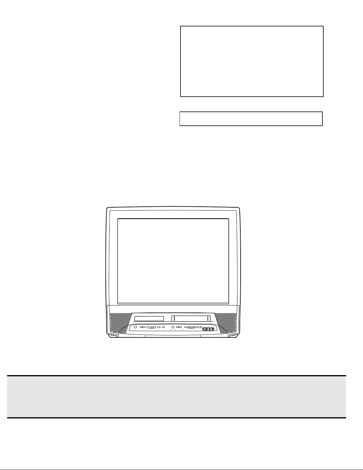
MANUAL 5885
Color TV with Built-In VCR/DVD Player
Service Manual
MAGNAVOX
Model: 27MDTR10S
Color TV with Built-In VCR/DVD Player
First Issue: 10/02
2002 Philips Consumer Electronics Company
Page 2

Philips Consumer Electronics Company
A Division of Philips Electronics North America Corporation
MANUAL 5885
Technical Service Data
Service Solutions Group
Technical Publications Dept.
P.O. Box 555, 401 E. Old Andrew Johnson Hwy.
Jefferson City,TN 37760
Sec. 1A: Main Section
( 27MDTR10S )
Specifications
Operating Instructions
Adjustment Procedures
Schematic Diagrams and CBA’s
Exploded Views
Cabinet & Electrical Parts Lists
Color TV with Built-In VCR/DVD Player
Service Manual
MAGNAVOX
Model: 27MDTR10S
Color TV with Built-In VCR/DVD Player
First Issue: 10/02
2002 Philips Consumer Electronics Company
Page 3

IMPORTANT SAFETY NOTICE
Proper service and repair is important to the safe, reliable operation of all
Philips Consumer Electronics Company** Equipment. The service procedures
recommended by Philips and described in this service manual are effective
methods of performing service operations. Some of these service operations
require the use of tools specially designed for the purpose. The special tools
should be used when and as recommended.
It is important to note that this manual contains various CAUTIONS and
NOTICES which should be carefully read in order to minimize the risk of personal injury to service personnel. The possibility exists that improper service
methods may damage the equipment. It also is important to understand that
these CAUTIONS and NOTICES ARE NOT EXHAUSTIVE. Philips could not
possibly know, evaluate and advise the service trade of all conceivable ways
in which service might be done or of the possible hazardous consequences of
each way. Consequently, Philips has not undertaken any such broad evaluation. Accordingly, a servicer who uses a service procedure or tool which is
not recommended by Philips must first satisfy himself thoroughly that neither
his safety nor the safe operation of the equipment will be jeopardized by the
service method selected.
** Hereafter throughout this manual, Philips Consumer Electronics Company
will be referred to as Philips.
WARNING
Critical components having special safety characteristics are identified
with a # by the Ref. No. in the parts list and enclosed within a broken
line* (where several critical components are grouped in one area) along
with the safety symbol # on the schematics or exploded views.
Use of substitute replacement parts which do not have the same specified
safety characteristics may create shock, fire, or other hazards.
Under no circumstances should the original design be modified or altered
without written permission from Philips. Philips assumes no liability,
express or implied, arising out of any unauthorized modification of
design. Servicer assumes all liability.
* Broken Line
Manufactured under license from Dolby Laboratories. "Dolby"
and the double-D symbol are trademarks of Dolby Laboratories.
"DTS" and "DTS Digital Out" are trademarks of Digital Theater Systems Inc.
Page 4

TABLE OF CONTENTS
[ Main Section ]
Page
SPECIFICATIONS . . . . . . . . . . . . . . . . . . . . . . . . . . . . . . . . . . . . . . . . . . . . . . . . . . . . . . . . . . . . . . . . . . . . . . . . . . . . 1-1-1
LASER BEAM SAFETY PRECAUTIONS . . . . . . . . . . . . . . . . . . . . . . . . . . . . . . . . . . . . . . . . . . . . . . . . . . . . . . . . . . 1-2-1
IMPORTANT SAFETY PRECAUTIONS . . . . . . . . . . . . . . . . . . . . . . . . . . . . . . . . . . . . . . . . . . . . . . . . . . . . . . . . . . . 1-3-1
STANDARD NOTES FOR SERVICING . . . . . . . . . . . . . . . . . . . . . . . . . . . . . . . . . . . . . . . . . . . . . . . . . . . . . . . . . . . . 1-4-1
PREPARATION FOR SERVICING. . . . . . . . . . . . . . . . . . . . . . . . . . . . . . . . . . . . . . . . . . . . . . . . . . . . . . . . . . . . . . . . 1-5-1
OPERATING CONTROLS AND FUNCTIONS . . . . . . . . . . . . . . . . . . . . . . . . . . . . . . . . . . . . . . . . . . . . . . . . . . . . . . 1-6-1
REMOTE CONTROL OPERATION . . . . . . . . . . . . . . . . . . . . . . . . . . . . . . . . . . . . . . . . . . . . . . . . . . . . . . . . . . . . . . . 1-7-1
CABINET DISASSEMBLY INSTRUCTIONS . . . . . . . . . . . . . . . . . . . . . . . . . . . . . . . . . . . . . . . . . . . . . . . . . . . . . . . . 1-8-1
ELECTRICAL ADJUSTMENT INSTRUCTIONS . . . . . . . . . . . . . . . . . . . . . . . . . . . . . . . . . . . . . . . . . . . . . . . . . . . . . 1-9-1
Adjustment Points and Test Points . . . . . . . . . . . . . . . . . . . . . . . . . . . . . . . . . . . . . . . . . . . . . . . . . . . . . . . . . . . . . 1-9-7
FIRMWARE RENEWAL MODE . . . . . . . . . . . . . . . . . . . . . . . . . . . . . . . . . . . . . . . . . . . . . . . . . . . . . . . . . . . . . . . . . . 1-10-1
BLOCK DIAGRAMS <TV/VCR SECTION>
Servo/System Control Block Diagram . . . . . . . . . . . . . . . . . . . . . . . . . . . . . . . . . . . . . . . . . . . . . . . . . . . . . . . . . . 1-11-1
Video Block Diagram . . . . . . . . . . . . . . . . . . . . . . . . . . . . . . . . . . . . . . . . . . . . . . . . . . . . . . . . . . . . . . . . . . . . . . . 1-11-3
Audio Block Diagram . . . . . . . . . . . . . . . . . . . . . . . . . . . . . . . . . . . . . . . . . . . . . . . . . . . . . . . . . . . . . . . . . . . . . . . 1-11-5
Hi-Fi Block Diagram . . . . . . . . . . . . . . . . . . . . . . . . . . . . . . . . . . . . . . . . . . . . . . . . . . . . . . . . . . . . . . . . . . . . . . . . 1-11-7
Chroma/Tuner Block Diagram . . . . . . . . . . . . . . . . . . . . . . . . . . . . . . . . . . . . . . . . . . . . . . . . . . . . . . . . . . . . . . . . 1-11-9
CRT/H.V. Block Diagram . . . . . . . . . . . . . . . . . . . . . . . . . . . . . . . . . . . . . . . . . . . . . . . . . . . . . . . . . . . . . . . . . . . . 1-11-11
Power Supply Block Diagram. . . . . . . . . . . . . . . . . . . . . . . . . . . . . . . . . . . . . . . . . . . . . . . . . . . . . . . . . . . . . . . . . 1-11-13
BLOCK DIAGRAMS <DVD SECTION>
DVD System Control Block Diagram . . . . . . . . . . . . . . . . . . . . . . . . . . . . . . . . . . . . . . . . . . . . . . . . . . . . . . . . . . . 1-11-15
RF Signal Process/Servo Block Diagram. . . . . . . . . . . . . . . . . . . . . . . . . . . . . . . . . . . . . . . . . . . . . . . . . . . . . . . . 1-11-17
DVD Signal Process Block Diagram. . . . . . . . . . . . . . . . . . . . . . . . . . . . . . . . . . . . . . . . . . . . . . . . . . . . . . . . . . . . 1-11-19
DVD Video Block Diagram . . . . . . . . . . . . . . . . . . . . . . . . . . . . . . . . . . . . . . . . . . . . . . . . . . . . . . . . . . . . . . . . . . . 1-11-21
DVD Audio Block Diagram . . . . . . . . . . . . . . . . . . . . . . . . . . . . . . . . . . . . . . . . . . . . . . . . . . . . . . . . . . . . . . . . . . . 1-11-23
SCHEMATIC DIAGRAMS / CBA’S AND TEST POINTS . . . . . . . . . . . . . . . . . . . . . . . . . . . . . . . . . . . . . . . . . . . . . . . 1-12-1
Main 1/4 Schematic Diagram Parts Location Guide<TV/VCR SECTION> . . . . . . . . . . . . . . . . . . . . . . . . . . . . . . 1-12-2
Main 1/4 Schematic Diagram <TV/VCR SECTION> . . . . . . . . . . . . . . . . . . . . . . . . . . . . . . . . . . . . . . . . . . . . . . . 1-12-3
Main 2/4 Schematic Diagram <TV/VCR SECTION> . . . . . . . . . . . . . . . . . . . . . . . . . . . . . . . . . . . . . . . . . . . . . . . 1-12-6
Main 2/4 Schematic Diagram Parts Location Guide <TV/VCR SECTION> . . . . . . . . . . . . . . . . . . . . . . . . . . . . . . 1-12-9
Main 3/4 Schematic Diagram Parts Location Guide <TV/VCR SECTION> . . . . . . . . . . . . . . . . . . . . . . . . . . . . . . 1-12-10
Main 3/4 Schematic Diagram <TV/VCR SECTION> . . . . . . . . . . . . . . . . . . . . . . . . . . . . . . . . . . . . . . . . . . . . . . . 1-12-11
Main 4/4 Schematic Diagram <TV/VCR SECTION> . . . . . . . . . . . . . . . . . . . . . . . . . . . . . . . . . . . . . . . . . . . . . . . 1-12-14
Main 4/4 Schematic Diagram Parts Location Guide <TV/VCR SECTION> . . . . . . . . . . . . . . . . . . . . . . . . . . . . . . 1-12-17
Main CBA Parts Location Guide <TV/VCR SECTION> . . . . . . . . . . . . . . . . . . . . . . . . . . . . . . . . . . . . . . . . . . . . . 1-12-19
Main CBA Top View <TV/VCR SECTION> . . . . . . . . . . . . . . . . . . . . . . . . . . . . . . . . . . . . . . . . . . . . . . . . . . . . . . 1-12-21
Main CBA Bottom View <TV/VCR SECTION>. . . . . . . . . . . . . . . . . . . . . . . . . . . . . . . . . . . . . . . . . . . . . . . . . . . . 1-12-24
CRT Schematic Diagram <TV/VCR SECTION> . . . . . . . . . . . . . . . . . . . . . . . . . . . . . . . . . . . . . . . . . . . . . . . . . . 1-12-27
CRT CBA Top/Bottom View <TV/VCR SECTION> . . . . . . . . . . . . . . . . . . . . . . . . . . . . . . . . . . . . . . . . . . . . . . . . 1-12-29
H.V. Schematic Diagram <TV/VCR SECTION> . . . . . . . . . . . . . . . . . . . . . . . . . . . . . . . . . . . . . . . . . . . . . . . . . . . 1-12-31
H.V. CBA Top View <TV/VCR SECTION> . . . . . . . . . . . . . . . . . . . . . . . . . . . . . . . . . . . . . . . . . . . . . . . . . . . . . . . 1-12-33
H.V. CBA Bottom View <TV/VCR SECTION> . . . . . . . . . . . . . . . . . . . . . . . . . . . . . . . . . . . . . . . . . . . . . . . . . . . . 1-12-35
Junction-A, B CBA Top/Bottom View <TV/VCR SECTION> . . . . . . . . . . . . . . . . . . . . . . . . . . . . . . . . . . . . . . . . . 1-12-37
Power Supply/AV Schematic Diagram Parts Location Guide <TV/VCR SECTION> . . . . . . . . . . . . . . . . . . . . . . . 1-12-38
Power Supply/AV Schematic Diagram <TV/VCR SECTION> . . . . . . . . . . . . . . . . . . . . . . . . . . . . . . . . . . . . . . . . 1-12-39
Power Supply/AV CBA Top View <TV/VCR SECTION>. . . . . . . . . . . . . . . . . . . . . . . . . . . . . . . . . . . . . . . . . . . . . 1-12-42
Power Supply/AV CBA Bottom View <TV/VCR SECTION>. . . . . . . . . . . . . . . . . . . . . . . . . . . . . . . . . . . . . . . . . . 1-12-45
DVD Main 1/4 Schematic Diagram <DVD SECTION> . . . . . . . . . . . . . . . . . . . . . . . . . . . . . . . . . . . . . . . . . . . . . . 1-12-48
DVD Main 2/4 Schematic Diagram <DVD SECTION> . . . . . . . . . . . . . . . . . . . . . . . . . . . . . . . . . . . . . . . . . . . . . . 1-12-51
DVD Main 3/4 Schematic Diagram <DVD SECTION> . . . . . . . . . . . . . . . . . . . . . . . . . . . . . . . . . . . . . . . . . . . . . . 1-12-54
DVD Main 4/4 Schematic Diagram <DVD SECTION> . . . . . . . . . . . . . . . . . . . . . . . . . . . . . . . . . . . . . . . . . . . . . . 1-12-57
Filter Schematic Diagram <DVD SECTION> . . . . . . . . . . . . . . . . . . . . . . . . . . . . . . . . . . . . . . . . . . . . . . . . . . . . . 1-12-59
Filter CBA Top/Bottom View <DVD SECTION> . . . . . . . . . . . . . . . . . . . . . . . . . . . . . . . . . . . . . . . . . . . . . . . . . . . 1-12-61
WAVEFORMS<TV/VCR SECTION> . . . . . . . . . . . . . . . . . . . . . . . . . . . . . . . . . . . . . . . . . . . . . . . . . . . . . . . . . . . . . . 1-13-1
WAVEFORMS<DVD SECTION>. . . . . . . . . . . . . . . . . . . . . . . . . . . . . . . . . . . . . . . . . . . . . . . . . . . . . . . . . . . . . . . . . 1-13-3
WIRING DIAGRAM <TV/VCR SECTION> . . . . . . . . . . . . . . . . . . . . . . . . . . . . . . . . . . . . . . . . . . . . . . . . . . . . . . . . . 1-14-1
WIRING DIAGRAM <DVD SECTION> . . . . . . . . . . . . . . . . . . . . . . . . . . . . . . . . . . . . . . . . . . . . . . . . . . . . . . . . . . . . 1-14-3
SYSTEM CONTROL TIMING CHARTS . . . . . . . . . . . . . . . . . . . . . . . . . . . . . . . . . . . . . . . . . . . . . . . . . . . . . . . . . . . 1-15-1
IC PIN FUNCTION . . . . . . . . . . . . . . . . . . . . . . . . . . . . . . . . . . . . . . . . . . . . . . . . . . . . . . . . . . . . . . . . . . . . . . . . . . . 1-16-1
LEAD IDENTIFICATIONS . . . . . . . . . . . . . . . . . . . . . . . . . . . . . . . . . . . . . . . . . . . . . . . . . . . . . . . . . . . . . . . . . . . . . . 1-17-1
ELECTRICAL PARTS LIST . . . . . . . . . . . . . . . . . . . . . . . . . . . . . . . . . . . . . . . . . . . . . . . . . . . . . . . . . . . . . . . . . . . . . 1-18-1
EXPLODED VIEWS . . . . . . . . . . . . . . . . . . . . . . . . . . . . . . . . . . . . . . . . . . . . . . . . . . . . . . . . . . . . . . . . . . . . . . . . . . 1-19-1
MECHANICAL PARTS LIST . . . . . . . . . . . . . . . . . . . . . . . . . . . . . . . . . . . . . . . . . . . . . . . . . . . . . . . . . . . . . . . . . . . . 1-20-1
Page 5

SPECIFICATIONS
*ˆMode---------SP mode unless otherwise specified
*Test input terminal
<Except Tuner>-------------Video input (1Vp-p)
Audio input (-10dB)
<Tuner>-----------------------Ant. input (80dBµV) Video: 87.5%
Audio: 25kHz dev (1kHz Sin)
<DEFLECTION>
Description Condition Unit Nominal Limit
1. Over Scan — % 90 5
Horizontal % — 15
2. Linearity
3. High Voltage — kV 29 —
<VIDEO & CHROMA>
Description Condition Unit Nominal Limit
Vertical % — 10
Center m/m — 0.4
1. Misconvergence
2. Tint Control Range — deg ±30 —
3. Contrast Control Range — dB 6 2
4. Brightness (100% White Full Field) Contrast: Max ft-L 25 18
5. Color Temperature — K 9200 —
Corner m/m — 2.5
Side m/m — 1.5
<DVD>
Measurement at TP
Description Condition Unit Nominal Limit
1. Horizontal Resolution (TDV-540 TIT.2 CHP.16) — Line 330 320
2. Video S/N at CN3400 (TDV-540 TIT.2 CHP.6) — dB 60 55
3. S/N Chroma at CN3400 AM — dB 58 53
(TDV-540 TIT.2 CHP.17) PM — dB 58 53
4. Audio Distortion (LPCM 48 kHz, W/LPF)
(PTD 1-NOR TIT.1 CHP.1)
L
R
%
0.03
0.03
0.07
0.07
5. Audio freq. response (LPCM 48kHz)
(PTD 1-NOR TIT.1 CHP.5 -- 10)
6. Audio S/N (LPCM 48KHz,W/LPF,A-WTD)
(PTD 1-NOR TIT.1 CHP.1 -- 2)
L, 20 Hz
R, 20 Hz
L, 20 kHz
R, 20 kHz
L
R
1-1-1 T601SP
dB 0 +4/-5
dB 100 85
Page 6

<VCR>
Description Condition Unit Nominal Limit
1. Horizontal Resolution (R/P, SP) Line 230 200
2. Jitter (Low) (R/P, SP) µS0.1 0.2
3. S/N Chroma AM(SP) (R/P, SP) dB 38 33
PM(SP) (R/P, SP) dB 38 33
4. Wow & Flutter (JIS, UNWTD) (R/P, SP) % 0.25 0.5
<TUNER>
Description Condition Unit Nominal Limit
1. Video S/N (80dBµV, TV4ch) — dB 45 40
2. Audio S/N (W/LPF) — dB 45 40
<NORMAL AUDIO>
All items are measured across 8Ω resistor at speaker output terminal.
Description Condition Unit Nominal Limit
1. Audio Output Power (R/P, SP) W 1.0 0.8
2. Audio S/N (W/LPF) (R/P, SP) dB 40 36
3. Audio distortion (W/LPF,-10dB 1kHz IN) (R/P, SP) % 3.0 5.0
4. Audio Freq. Response (-10dB 1kHz IN) 200 Hz (R/P, SP) dB -2.0 -2.0±5.0
8 kHz (R/P, SP) dB 0 0±6.0
<Hi-Fi AUDIO>
* All items are measured at TP1701 and TP1702.
Description Condition Unit Nominal Limit
1. Output Level (-10dB 1kHz IN) (R/P, SP) dB -8.0 -8±4
2. Audio Distortion (-10dB 1kHz IN) (R/P, SP) % 0.5 1.0
3. Freq. Response (-15dB 1kHz IN) 20 Hz (R/P, SP) dB 0 ±4
20 kHz (R/P, SP) dB 0 ±4
Note: Nominal specifications represent the design specifications. All units should be able to approximate these.
Some will exceed and some may drop slightly below these specifications. Limit specifications represent the absolute worst condition that still might be considered acceptable. In no case should a unit fail to meet limit specifications.
1-1-2 T601SP
Page 7
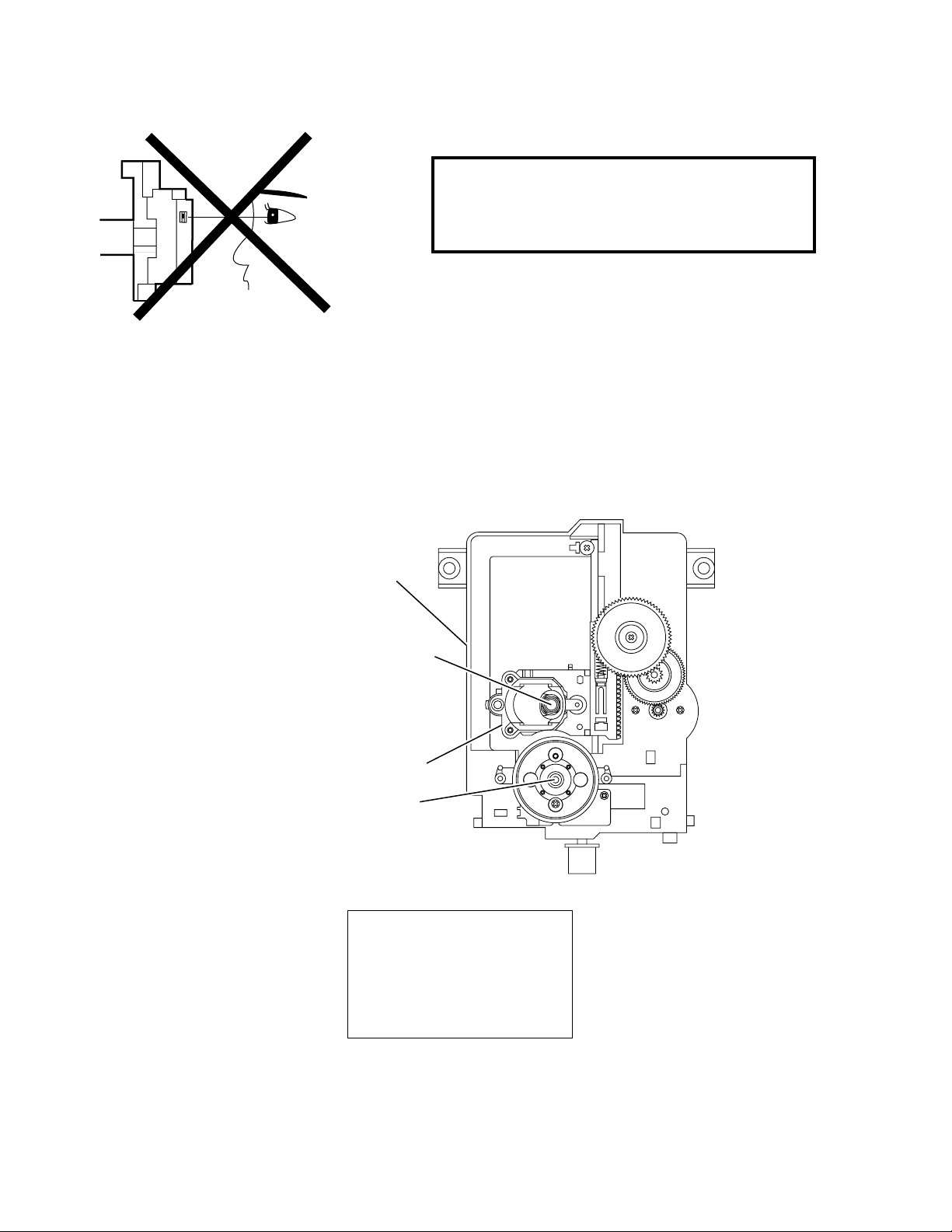
LASER BEAM SAFETY PRECAUTIONS
This DVD player uses a pickup that emits a laser beam.
Do not look directly at the laser beam coming
from the pickup or allow it to strike against
your skin.
The laser beam is emitted from the location shown in the figure. When checking the laser diode, be sure to keep
your eyes at least 30cm away from the pickup lens when the diode is turned on. Do not look directly at the laser
beam.
Caution: Use of controls and adjustments, or doing procedures other than those specified herein, may result in
hazardous radiation exposure.
Drive Mecha Assembly
Laser Beam Radiation
Laser Pickup
Turntable
LASER RADIATION
WHEN OPEN. DO NOT
STARE INTO BEAM.
CAUTION
Location: Inside Top of DVD mechanism.
1-2-1 DVD_LASER
Page 8

IMPORTANT SAFETY PRECAUTIONS
Product Safety Notice
Some electrical and mechanical parts have special
safety-related characteristics which are often not evident from visual inspection, nor can the protection
they give necessarily be obtained by replacing them
with components rated for higher voltage, wattage,
etc. Parts that have special safety characteristics are
identified by a # on schematics and in parts lists. Use
of a substitute replacement that does not have the
same safety characteristics as the recommended
replacement part might create shock, fire, and/or other
hazards. The Product’s Safety is under review continuously and new instructions are issued whenever
appropriate. Prior to shipment from the factory, our
products are carefully inspected to confirm with the
recognized product safety and electrical codes of the
countries in which they are to be sold. However, in
order to maintain such compliance, it is equally important to implement the following precautions when a set
is being serviced.
Precautions during Servicing
A. Parts identified by the # symbol are critical for
safety. Replace only with part number specified.
B. In addition to safety, other parts and assemblies
are specified for conformance with regulations
applying to spurious radiation. These must also be
replaced only with specified replacements.
Examples: RF converters, RF cables, noise blocking capacitors, and noise blocking filters, etc.
C. Use specified internal wiring. Note especially:
1)Wires covered with PVC tubing
2)Double insulated wires
3)High voltage leads
D. Use specified insulating materials for hazardous
live parts. Note especially:
1)Insulation tape
2)PVC tubing
3)Spacers
4)Insulators for transistors
E. When replacing AC primary side components
(transformers, power cord, etc.), wrap ends of
wires securely about the terminals before soldering.
F. Observe that the wires do not contact heat produc-
ing parts (heatsinks, oxide metal film resistors, fusible resistors, etc.).
G. Check that replaced wires do not contact sharp
edges or pointed parts.
H. When a power cord has been replaced, check that
5 - 6 kg of force in any direction will not loosen it.
I. Also check areas surrounding repaired locations.
J. Be careful that foreign objects (screws, solder
droplets, etc.) do not remain inside the set.
K. Crimp type wire connector
The power transformer uses crimp type connectors
which connect the power cord and the primary side
of the transformer. When replacing the transformer,
follow these steps carefully and precisely to prevent shock hazards.
Replacement procedure
1)Remove the old connector by cutting the wires at a
point close to the connector.
Important: Do not re-use a connector. (Discard it.)
2)Strip about 15 mm of the insulation from the ends
of the wires. If the wires are stranded, twist the
strands to avoid frayed conductors.
3)Align the lengths of the wires to be connected.
Insert the wires fully into the connector.
4)Use a crimping tool to crimp the metal sleeve at its
center. Be sure to crimp fully to the complete closure of the tool.
L. When connecting or disconnecting the internal con-
nectors, first, disconnect the AC plug from the AC
outlet.
1-3-1 DVD_SFN1
Page 9

Safety Check after Servicing
Examine the area surrounding the repaired location for
damage or deterioration. Observe that screws, parts,
and wires have been returned to their original positions. Afterwards, do the following tests and confirm
the specified values to verify compliance with safety
standards.
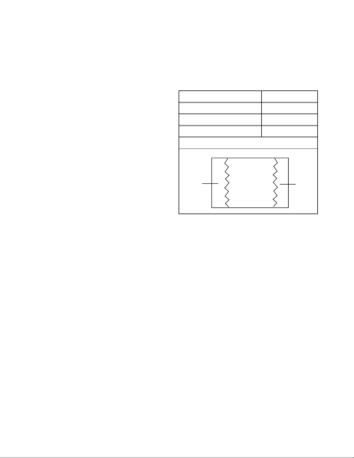
1. Clearance Distance
When replacing primary circuit components, confirm
specified clearance distance (d) and (d’) between soldered terminals, and between terminals and surrounding metallic parts. (See Fig. 1)
Table 1 : Ratings for selected area
AC Line Voltage Clearance Distance (d) (d’)
Chassis or Secondary Conductor
Primary Circuit Terminals
dd'
120 V
Note: This table is unofficial and for reference only.
Be sure to confirm the precise values.
2. Leakage Current Test
Confirm the specified (or lower) leakage current
between B (earth ground, power cord plug prongs)
and externally exposed accessible parts (RF terminals, antenna terminals, video and audio input and
output terminals, microphone jacks, earphone jacks,
etc.) is lower than or equal to the specified value in the
table below.
Measuring Method (Power ON) :
Insert load Z between B (earth ground, power cord
plug prongs) and exposed accessible parts. Use an
AC voltmeter to measure across the terminals of load
Z. See Fig. 2 and the following table.
Table 2: Leakage current ratings for selected areas
AC Line Voltage Load Z Leakage Current (i) Earth Ground (B) to:
120 V
≥ 3.2mm (0.126 inches)
0.15µF CAP. & 1.5kΩ RES.
Connected in parallel
Exposed Accessible Part
Z
1.5k
i≤0.5mA Peak Exposed accessible parts
0.15 F
Earth Ground
B
Power Cord Plug Prongs
AC Voltmeter
(High Impedance)
Fig. 1
Fig. 2
Note: This table is unofficial and for reference only. Be sure to confirm the precise values.
1-3-2 DVD_SFN1
Page 10

STANDARD NOTES FOR SERVICING
Circuit Board Indications
a. The output pin of the 3 pin Regulator ICs is indi-
cated as shown.
Top View
Out
b. For other ICs, pin 1 and every fifth pin are indicated
as shown.
Input
In
Pin 1
c. The 1st pin of every male connector is indicated as
shown.
Pin 1
Bottom View
5
10
How to Remove / Install Flat Pack-IC
1. Removal
With Hot-Air Flat Pack-IC Desoldering Machine:.
(1) Prepare the hot-air flat pack-IC desoldering
machine, then apply hot air to the Flat Pack-IC
(about 5 to 6 seconds). (Fig. S-1-1)
Fig. S-1-1
(2) Remove the flat pack-IC with tweezers while apply-
ing the hot air.
(3) Bottom of the flat pack-IC is fixed with glue to the
CBA; when removing entire flat pack-IC, first apply
soldering iron to center of the flat pack-IC and heat
up. Then remove (glue will be melted). (Fig. S-1-6)
(1) Release the flat pack-IC from the CBA using twee-
zers. (Fig. S-1-6)
Instructions for Connectors
1. When you connect or disconnect the FFC (Flexible
Foil Connector) cable, be sure to first disconnect
the AC cord.
2. FFC (Flexible Foil Connector) cable should be
inserted parallel into the connector, not at an angle.
FFC Cable
Connector
CBA
* Be careful to avoid a short circuit.
Caution:
1. Do not supply hot air to the chip parts around the
flat pack-IC for over 6 seconds because damage to
the chip parts may occur. Put masking tape around
the flat pack-IC to protect other parts from damage.
(Fig. S-1-2)
2. The flat pack-IC on the CBA is affixed with glue, so
be careful not to break or damage the foil of each
pin or the solder lands under the IC when removing
it.
Hot-air
Flat Pack-IC
Desoldering
CBA
Masking
Tape
Tweezers
Machine
Flat Pack-IC
Fig. S-1-2
1-4-1 DVD_NOTE
Page 11

With Soldering Iron:
(1) Using desoldering braid, remove the solder from all
pins of the flat pack-IC. When you use solder flux
which is applied to all pins of the flat pack-IC, you
can remove it easily. (Fig. S-1-3)
Flat Pack-IC
Desoldering Braid
(4) Bottom of the flat pack-IC is fixed with glue to the
CBA; when removing entire flat pack-IC, first apply
soldering iron to center of the flat pack-IC and heat
up. Then remove (glue will be melted). (Fig. S-1-6)
(5) Release the flat pack-IC from the CBA using twee-
zers. (Fig. S-1-6)
Note:
When using a soldering iron, care must be taken
to ensure that the flat pack-IC is not being held by
glue. When the flat pack-IC is removed from the
CBA, handle it gently because it may be damaged
if force is applied.
Soldering Iron
Fig. S-1-3
(2) Lift each lead of the flat pack-IC upward one by
one, using a sharp pin or wire to which solder will
not adhere (iron wire). When heating the pins, use
a fine tip soldering iron or a hot air desoldering
machine. (Fig. S-1-4)
Sharp
Pin
Fine Tip
Soldering Iron
Fig. S-1-4
(3) Bottom of the flat pack-IC is fixed with glue to the
CBA; when removing entire flat pack-IC, first apply
soldering iron to center of the flat pack-IC and heat
up. Then remove (glue will be melted). (Fig. S-1-6)
(4) Release the flat pack-IC from the CBA using twee-
zers. (Fig. S-1-6)
With Iron Wire:
(1) Using desoldering braid, remove the solder from all
pins of the flat pack-IC. When you use solder flux
which is applied to all pins of the flat pack-IC, you
can remove it easily. (Fig. S-1-3)
(2) Affix the wire to a workbench or solid mounting
point, as shown in Fig. S-1-5.
(3) While heating the pins using a fine tip soldering
iron or hot air blower, pull up the wire as the solder
melts so as to lift the IC leads from the CBA contact
pads as shown in Fig. S-1-5
To Solid
Mounting Point
CBA
Tweezers
Hot Air Blower
or
Iron Wire
Soldering Iron
Fig. S-1-5
Fine Tip
Soldeing Iron
Flat Pack-IC
Fig. S-1-6
1-4-2 DVD_NOTE
Page 12

2. Installation
(1) Using desoldering braid, remove the solder from
the foil of each pin of the flat pack-IC on the CBA
so you can install a replacement flat pack-IC more
easily.
(2) The “I” mark on the flat pack-IC indicates pin 1.
(See Fig. S-1-7.) Be sure this mark matches the 1
on the PCB when positioning for installation. Then
presolder the four corners of the flat pack-IC. (See
Fig. S-1-8.)
(3) Solder all pins of the flat pack-IC. Be sure that none
of the pins have solder bridges.
Example :
Pin 1 of the Flat Pack-IC
is indicated by a " ● " mark.
Fig. S-1-7
Instructions for Handling
Semi-conductors
Electrostatic breakdown of the semi-conductors may
occur due to a potential difference caused by electrostatic charge during unpacking or repair work.
1. Ground for Human Body
Be sure to wear a grounding band (1MΩ) that is properly grounded to remove any static electricity that may
be charged on the body.
2. Ground for Workbench
(4) Be sure to place a conductive sheet or copper plate
with proper grounding (1MΩ) on the workbench or
other surface, where the semi-conductors are to be
placed. Because the static electricity charge on
clothing will not escape through the body grounding band, be careful to avoid contacting semi-conductors with your clothing.
< Incorrect >
CBA
Presolder
Flat Pack-IC
Fig. S-1-8
CBA
< Correct >
Grounding Band
1MΩ
CBA
1MΩ
Conductive Sheet or
Copper Plate
1-4-3 DVD_NOTE
Page 13
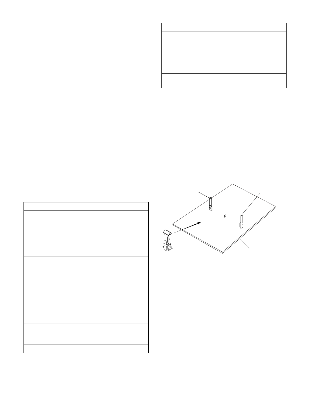
PREPARATION FOR SERVICING
How to Enter the Service Mode
Caution: 1
Optical sensors are used for Tape Start and End Sensor on this equipment. Read this page carefully and
prepare as described on this page before starting to
service; otherwise, the unit may operate unexpectedly.
Preparing: 1
Cover Q202 (START SENSOR) and Q201 (END SENSOR) with Insulation Tape or enter the Service Mode
to activate Sensor Inhibition automatically.
Note: Avoid playing, rewinding or fast forwarding the
tape to its beginning or end, because both Tape End
Sensors are not active.
How to Enter the Service Mode
1. Turn power on.
2. Use service remote control unit and press WAKEUP/SLEEP key. (See page 1-9-1)
3. When entering the Service Mode, one of the number (1, 2 or 4) will display at corners of the screen.
4. During the Service Mode, electrical adjustment
mode can be selected by remote control key. (Service remote control unit).
Details are as follows.
Key Adjustment Mode
Purity check mode: Shows Red,
7
8
9
Caution: 2
The deck mechanism assembly is mounted on the
Main CBA directly, and SW1211 (REC-SAFETY SW)
is mounted on the Main CBA. When deck mechanism
assembly is removed from the Main CBA due to servicing, this switch can not be operated automatically.
Green, Blue or White cyclically on the
screen each time the “7” key is
pressed.
H. Shift adjustment mode: See adjustment instructions page 1-9-3.
V.size/V. shift adjustment: See adjustment instructions pages 1-9-2 & 1-9-3.
Preparing: 2
1. To eject the tape, press the STOP/EJECT button
on the unit (or Remote Control).
2. When you want to record during the Service mode,
press the Rec button while depressing SW1211
(REC-SAFETY SW) on the Main CBA.
Q201
(END SENSOR)
Q202
(START SENSOR)
Key Adjustment Mode
Picture adjustment mode: Press the
MENU button to change from BRT
(Bright), *CNT (Contrast), *CLR
MENU
0 No need to use.
1 No need to use.
2
3
4
5
6 No need to use.
(Color), *TNT(Tint) and *V-T. Press
CH UP/DOWN key to display Initial
Value. *Marked items are not necessary to adjust normally.
AGC/H adjustment mode: See adjustment instructions page 1-9-2.
Auto AFT adjustment mode: See
adjustment instructions page 1-9-2.
Auto record mode: Perform recording
(15 Sec.)-->Stop-->Rewind (Zero
return) automatically.
Head switching point adjustment
mode: See adjustment instructions
page 1-9-5.
SW1211
(REC-SAFETY SW)
MAIN CBA
1-5-1 TD603PFS
Page 14
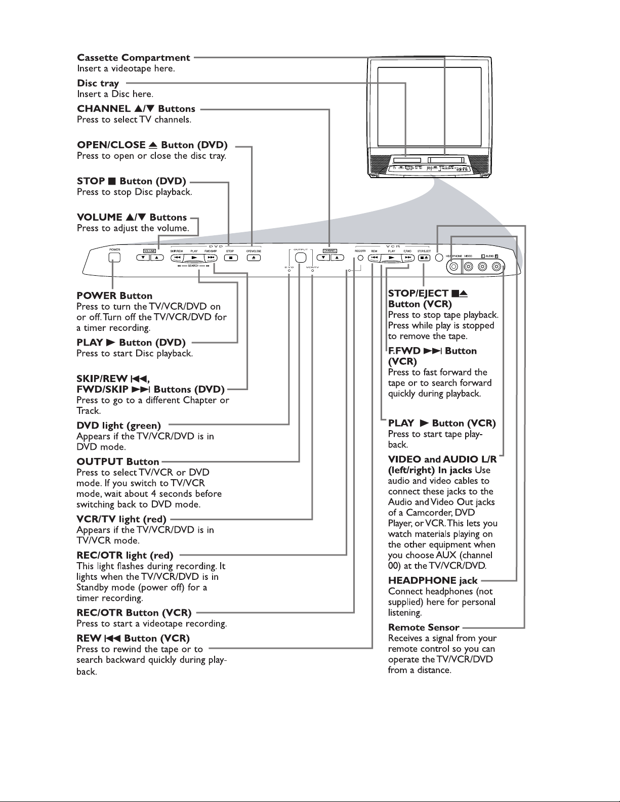
OPERATING CONTROLS AND FUNCTIONS
1-6-1 TD603IB
Page 15

1-6-2 TD603IB
Page 16

REMOTE CONTROL OPERATION
1-7-1 TD603IBR
Page 17

1-7-2 TD603IBR
Page 18

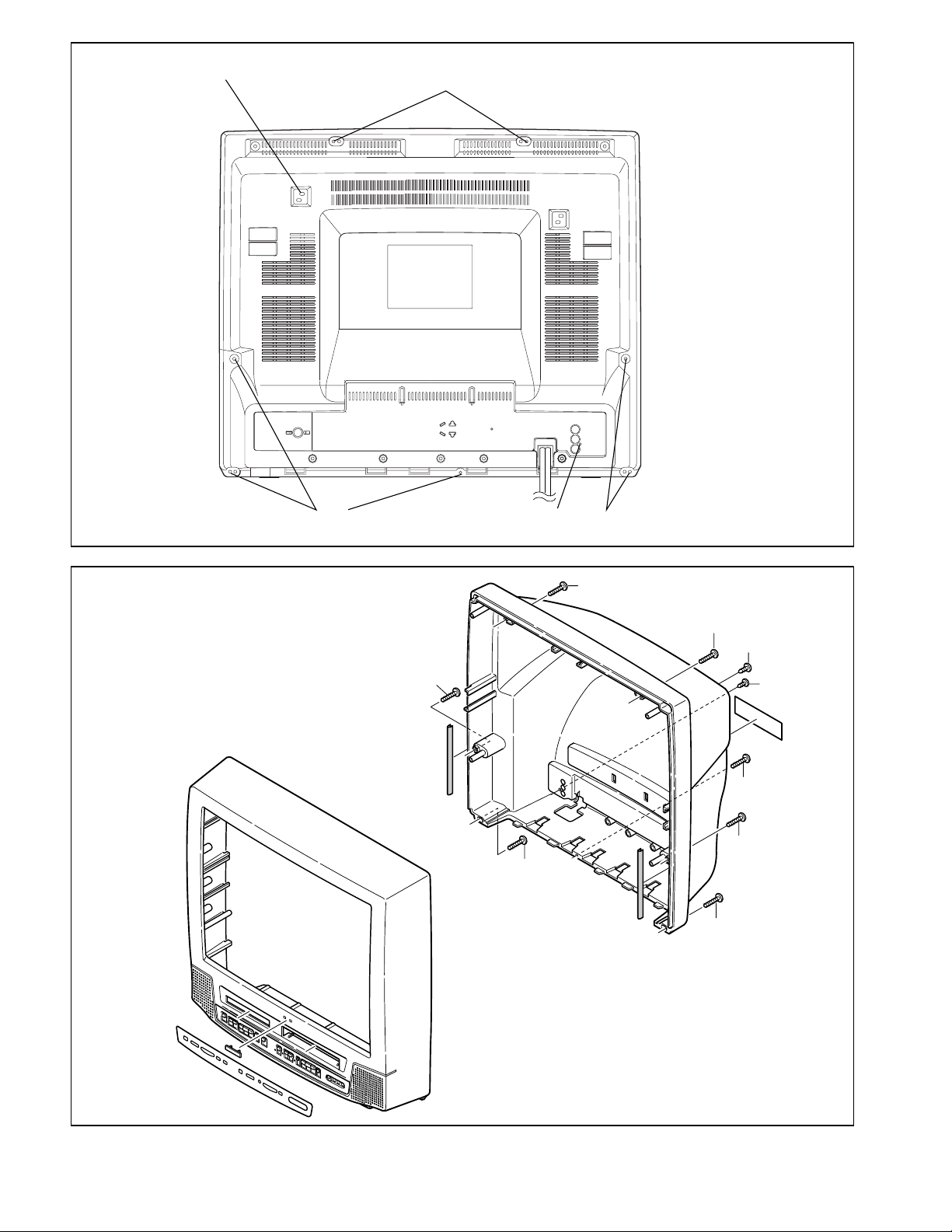
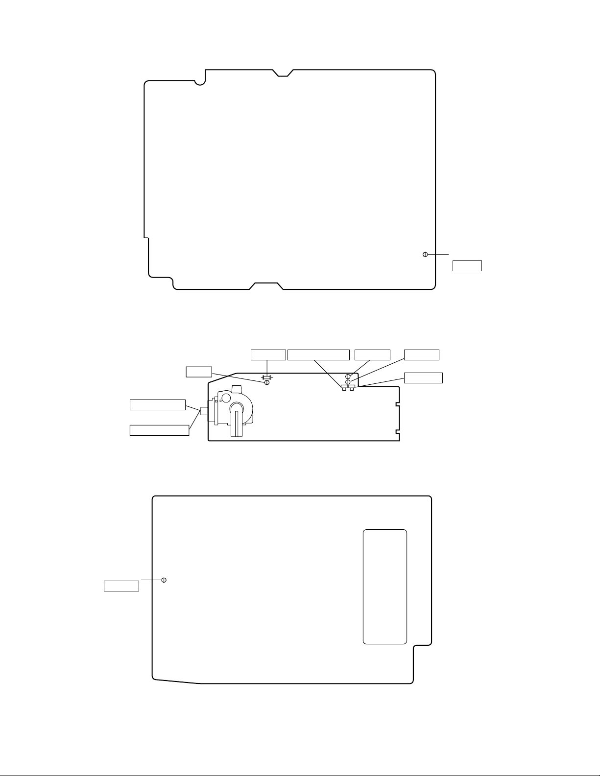
CABINET DISASSEMBLY INSTRUCTIONS
1. Disassembly Flowchart
This flowchart indicates the disassembly steps for the
cabinet parts and the CBA in order to gain access to
item(s) to be serviced. When reassembling, follow the
steps in reverse order. Bend, route and dress the
cables as they were.
Caution!
When removing the CRT, be sure to discharge the
Anode Lead of the CRT with the CRT Ground Wire
before removing the Anode Cap.
[1] Rear Cabinet
[2] H.V. CBA
[4] CRT
[5] Shield Box
[6] DVD Mechanism
MAIN
CBA UNIT
[9] Bottom Plate
[3] Tray Chassis Unit
[11] Deck Assembly
[12] Main CBA
[8] Filter CBA[7] DVD
REMOVAL
ID/
LOC.
No.
PAR T
REMOVE/
*UNHOOK/UNLOCK/
Fig.
No.
RELEASE/UNPLUG/
DESOLDER
[7]
DVD Main
CBA Unit
3(S-7), CN101,
5
CN401
[8] Filter CBA 3, 6 CN401, CN402 -
Bottom
[9]
[10]
[11]
Plate
Power
Supply/AV
CBA
Deck
Assembly
3 6(S-8) -
3(S-9), CN2802,
3, 6
CN2803, CN2804
7(S-10), 2(S-11),
CL1201, CL1401,
3, 6
CL1402, CL1403
[12] Main CBA 3 3(S-12) -
↓
(1)
↓
(2)
↓
(3)
↓
(4)
Note
2-1
2-2
2-3
3
-
4
↓
(5)
[10] Power Supply/AV CBA
2. Disassembly Method
REMOVAL
ID/
LOC.
PART
No.
Rear
[1]
Cabinet
H.V. CBA
[2]
(With
Holder)
Tr ay
[3]
Chassis
Unit
[4] CRT 4 4(S-4) -
[5] Shield Box 3 5(S-5) -
REMOVE/
*UNHOOK/UNLOCK/
Fig.
No.
RELEASE/UNPLUG/
DESOLDER
1, 2 7(S-1), 1(S-2), 1(S-3) -
Anode Cap, CN501,
3, 4,
CRT CBA, CN571,
6
CN1301, CN1302,
CN2602
CN1802, CN2801,
3, 6
CN2601
Note
1
-
(1): Order of steps in Procedure. When reassembling,
follow the steps in reverse order.These numbers
are also used as the Identification (location) No. of
parts in Figures.
(2): Parts to be removed or installed.
(3): Fig. No. showing Procedure of Part Location.
(4): Identification of part to be removed, unhooked,
unlocked, released, unplugged, unclamped, or
desoldered.
S=Screw, P=Spring, L=Locking Tab, CN=Connec-
tor, *=Unhook, Unlock, Release, Unplug, or Desol-
der
2(S-2) = two screws (S-2)
(5): Refer to the following Reference Notes in the
Table.
[6]
DVD
Mechanism
CN501, CN701,
3, 6
3(S-6)
-
1-8-1 TD603DC
Page 19

Reference Notes in the Table
Caution !
When removing the CRT, be sure to discharge the
Anode Lead of the CRT with the CRT Ground Wire
before removing the Anode Cap.
Reference Notes in the Table
CAUTION 1: Discharge the Anode Lead of the CRT
with the CRT Ground Wire before removing the Anode
Cap.
1. Disconnect the following: Anode Cap, CN501, CRT
CBA, CN571, CN2602, CN1301 and CN1302.
Then remove H.V. CBA (with Holder).
CAUTION 2: Electrostatic breakdown of the laser
diode in the optical system block may occur as a
potential difference caused by electrostatic charge
accumulated on cloth, human body etc., during
unpacking or repair work.
To avoid damage of pickup follow next procedures.
2-1. Slide the pickup unit as shown in Fig. 5.
2-2. Short either of the two type three short lands with
solder before removing the FFC cable (CN101)
from it. If you disconnect the FFC cable (CN101),
the laser diode of pickup will be destroyed. (Fig.
5)
2-3. Disconnect Connector (CN401). Remove screws
3(S-7) and lift the DVD Main CBA Unit. (Fig. 5)
CAUTION 3: When reassembling, confirm the FFC
cable (CN101) is connected completely. Then remove
the solder from the three short lands. (Fig. 5)
4. Remove screws 7(S-10) and 2(S-11). Then, desolder connectors (CL1201, CL1401, CL1402,
CL1403) and lift up the Deck Assembly.
1-8-2 TD603DC
Page 20
S-2
S-1
[1] REAR CABINET
S-1
S-1
S-1
S-3
S-1
S-1
[1] REAR CABINET
Fig. 1
S-1
S-3
S-2
S-1
S-1
S-1
Fig. 2
1-8-3 TD603DC
Page 21

S-5
S-5
[8] Filter
CBA
S-8
[9] Bottom
Plate
S-8
S-6
[6] DVD
Mechanism
S-9
[5] Shield Box
S-8
S-9
S-10
[3] Tray Chassis
S-10
[11] Deck
Assembly
S-10
S-12
H.V. CBA
[10] Power
Supply/
AV CBA
S-11
[2] H.V. CBA
[12] Main CBA
S-11
(wih Holder)
Fig. 3
1-8-4 TD603DC
Page 22

S-4
Anode Cap
CRT CBA
S-4
Type A
[4] CRT
S-4
S-4
Fig. 4
Three short lands
CN101
S-7
CN401
S-7
B
[7] DVD Main
CBA Unit
A
DVD Mechanism
Type B
Slide
Pickup Unit
View for B
View for A
Three short lands
C
View for C
Fig. 5
1-8-5 TD603DC
Page 23
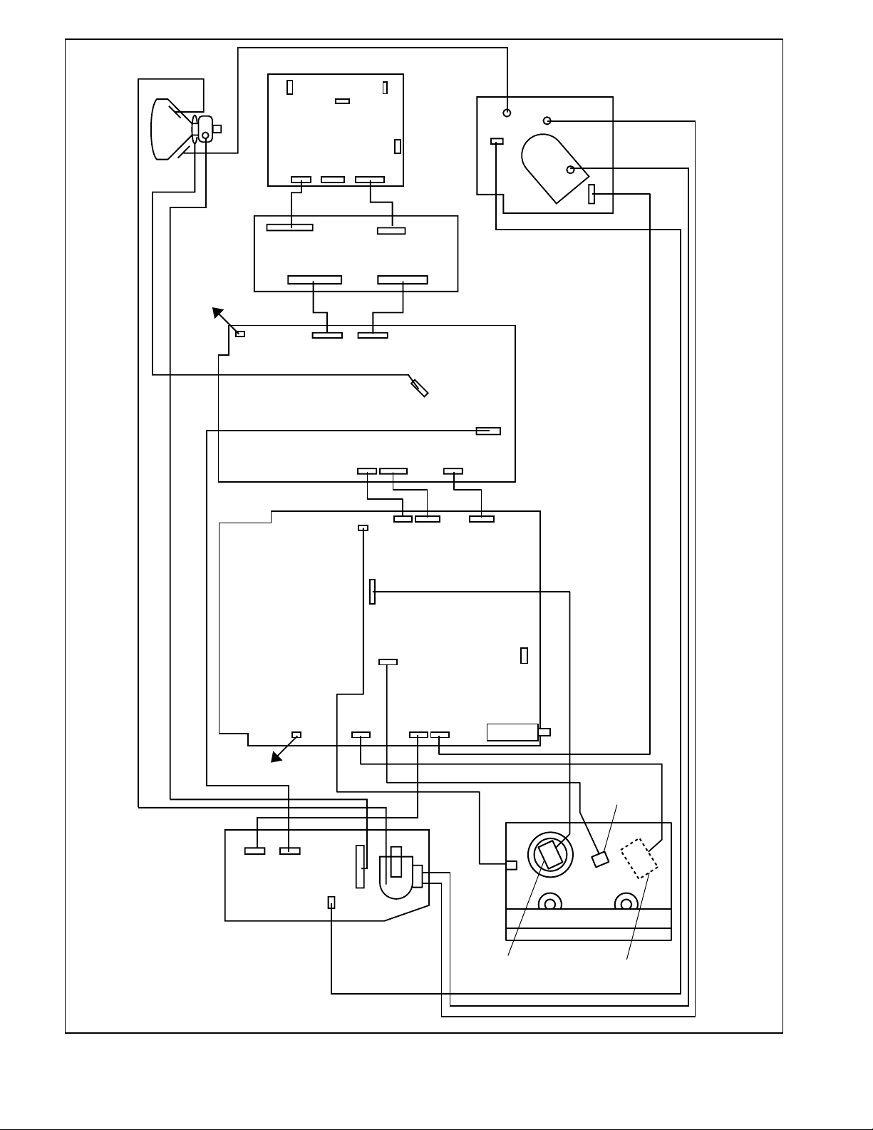
ANODE
CRT
GND
DVD MAIN CBA
FACTORY USE
ONLY
CN501 CN101
CN401
CN701
CL501
CRT CBA
CN501
SCREEN
FOCUS
CL504A
TO
SPEAKER
CN403
CN401
CN2801
CN2401 CN2402
POWER SUPPLY/
AV CBA
CN2802
CL1403
MAIN CBA
CN404
CN402
CN2803
CN1805
CL1401
CL1402
FILTER CBA
CN2601
CN2602
CN2804
CN1804
CN1803
INT MON
FACTORY USE
ONLY
CN1303
H.V. CBA
CN1802
TO SPEAKER
CL503A
CL501A
CL502A
CN571
CL1201
CN1302
CN1301
FE HEAD
CYLINDER
ASSEMBLY
TUNER
AC HEAD
ASSEMBLY
DECK ASSEMBLY
CAPSTAN
MOTOR
Fig. 6
1-8-6 TD603DC
Page 24

ELECTRICAL ADJUSTMENT INSTRUCTIONS
General Note:
"CBA" is abbreviation for "Circuit Board
Assembly."
NOTE:
Electrical adjustments are required after replacing
circuit components and certain mechanical parts.
It is important to perform these adjustments only
after all repairs and replacements have been completed.
Also, do not attempt these adjustments unless the
proper equipment is available.
Test Equipment Required
1. NTSC Pattern Generator (Color Bar W/White Window, Red Color, Dot Pattern, Gray Scale, Monoscope, Multi-Burst)
2. AC Milli Voltmeter (RMS)
3. Alignment Tape (VFMS0001H6), Blank Tape
4. DC Voltmeter
5. Oscilloscope: Dual-trace with 10:1 probe,
V-Range: 0.001~50V/Div,
F-Range: DC~AC-60MHz
6. Frequency Counter
7. Plastic Tip Driver
How to Set Up the Service Mode:
Service Mode:
1. Use the service remote control unit.
2. Turn the power on. (Use main power on the TV
unit.)
3. To enter the TV mode, press "CH o" or "CH p"
button on the TV unit.
4. Press "DISC MENU" button on the service remote
control unit. (Version of micro computer will display
on the CRT. (Ex: 057-001)
X-Ray Protection Test
X-Ray protection test should be done when replacing
any parts of this chassis.
1. Short test points J520 and J522 (on H.V. CBA.)
2. Confirm that the main power turns off.
3. If the main power does not turn off, then replace
the following parts (D591, Q591, R592, R593,
R594 and IC1201.)
4. Perform steps 1 to 3 again.
1. DC 120V (+B) Adjustment
Purpose: To obtain correct operation.
Symptom of Misadjustment: The picture is dark and
unit does not operate correctly.
How to make service remote control
unit:
1. Prepare normal remote control unit. (ID No.
NE206UD, Part No. 4835 218 37345) Remove 4
screws from the back lid. (Fig. 1)
2. Add J1 (Jumper Wire) to the remote control CBA.
(Fig. 2)
SCREW
Remote control unit (Bottom)
J 1
Fig. 1
Test Point Adj. Point
J523(+B)
HEAT SINK (on H.V. CBA)
(GND)
M. EQ. Spec.
DC Voltmeter +120±0.5V DC
Notes: J523(+B), HEAT SINK --- H.V. CBA
VR2601 --- Power Supply/AV CBA
1. Connect the unit to AC power outlet.
2. Connect DC Volt Meter to J523(+B) and HEAT
SINK (on H.V. CBA) (GND).
3. Adjust VR2601 so that the voltage of J523(+B)
becomes +120±0.5V DC.
VR2601
Remote control CBA
Fig. 2
1-9-1 TD603EA
Page 25
2. Auto AFT (VCO) Adjustment
4. H Adjustment
Purpose: To operate AFT correctly.
Symptom of Misadjustment: AFT does not work cor-
rectly and/or synchronization is faulty.
1. Set the unit to the Video mode with no signal input.
2. Enter the Service Mode. (See page 1-9-1.) Then
press number "3" button on the service remote
control unit.
3. If the screen color changes to "Green" then this
adjustment is finished.
4. If the screen color changes to "Red" then this
adjustment is failed. Repeat steps 1 and 2 or check
relative circuit or parts (IC).
3. TV AGC Adjustment
Purpose: Set AGC (Auto Gain Control) Level.
Symptom of Misadjustment: AGC does not synchro-
nize correctly when RF input level is too weak and picture distortion may occur if it is too strong.
Test Point Adj. Point Input
TP1001
(AGC)
CH o / p
buttons
M. EQ. Spec.
Color Bar 67.25MHz
60dBµV
Purpose: To get correct horizontal position and size
of screen image.
Symptom of Misadjustment: Horizontal position and
size of screen image may not be properly displayed.
Test Point Adj. Point Mode
R583 CH o / p buttons Video
M. EQ. Spec.
Frequency Counter 15.734kHz±300Hz
Note: R583 --- H.V. CBA
1. Connect frequency counter to R583.
2. Operate the unit for at least 20 minutes.
3. Enter the Service Mode. (See page 1-9-1.) Press
"2" button on the service remote control unit and
select H-ADJ Mode. (Press "2" button then display
will change H-ADJ and AGC.)
4. Press "CH o / p" buttons on the service remote
control unit so that the display will change "0" to
"7." At this moment, choose display "0" to "7" when
the frequency counter display is closest to
15.734kHz±300Hz.
5. Turn the power off and on again.
Pattern Generator
DC Voltmeter
Note: TP1001--- Main CBA
1. Enter the Service Mode. (See page 1-9-1.) Then
press "2" button on the service remote control unit
and select AGC mode.
2. Receive the Color Bar signal for channel 4
(67.25MHz). (RF Input Level: 60dBµV)
3. Press "CH o / p" buttons so that the voltage of
TP1001 (AGC) becomes +2.8V±0.3V DC.
4. Turn the power off and on again.
+2.8±0.3V DC
5. V. Size Adjustment
Purpose: To obtain correct vertical height of screen
image.
Symptom of Misadjustment: If V. Size is incorrect,
vertical height of image on the screen may not be
properly displayed.
Adj. Point Input
CH o / p buttons Monoscope
M. EQ. Spec.
Pattern Generator 90±5%
1. Enter the Service Mode. (See page 1-9-1.)
Press "9" button on the service remote control unit
and select V-S Mode. (Press "9" button then display will change to V-P and V-S).
2. Input monoscope pattern.
3. Press "CH o / p" buttons on the service remote
control unit so that the monoscope pattern is
90±5% of display size and the circle is round.
1-9-2 TD603EA
Page 26
6. V. Shift Adjustment
8. Cut-off Adjustment
Purpose: To obtain correct vertical position of screen
image.
Symptom of Misadjustment: If V. shift is incorrect,
vertical position of image on the screen may not be
properly displayed.
Adj. Point Input
CH o / p buttons Monoscope
M. EQ.
Pattern Generator
1. Enter the Service Mode. (See page 1-9-1.)
Press "9" button on the service remote control unit
and select V-P Mode. (Press "9" button then display
will change to V-P and V-S).
2. Input monoscope pattern.
3. Press "CH o / p" buttons on the service remote
control unit so that the top and bottom of the monoscope pattern are equal to each other.
7. H. Shift Adjustment
Purpose: To adjust the beam current of R, G, B, and
screen voltage.
Symptom of Misadjustment: White color may be
reddish, greenish or bluish.
Adj. Point Mode Input
Screen-Control Ext.
M. EQ. Spec.
Pattern Generator
Color Analyzer
Figure
PATTERN
GENERATOR
Black Raster /
White Raster
See Reference
Notes below
Purpose: To obtain correct horizontal position and
size of screen image.
Symptom of Misadjustment: Horizontal position and
size of screen image may not be properly displayed.
Adj. Point Input
CH o / p buttons Monoscope
M. EQ.
Pattern Generator
1. Enter the Service Mode. (See page 1-9-1.)
Press "8" button on the service remote control unit
and select H-P Mode.
2. Input monoscope pattern.
3. Press "CH o / p" buttons on the service remote
control unit so that the left and right side of the
monoscope pattern are equal to each other.
4. Turn the power off and on again.
EXT. INPUT
Color Analyzer
Fig. 3
Notes: Screen Control FBT --- H.V. CBA
FBT= Fly Back Transformer
Use the service remote control unit
1. Degauss the CRT and allow CRT to operate for 20
minutes before starting the alignment.
2. Input the Black raster signal from EXT. input.
3. Enter the Service Mode. (See page 1-9-1.)
4. Press the "VOL p" button.
(Press "VOL p" then display will change CUT OFF/
DRIVE, VCO adjustment, 7Fh adjustment).
5. Choose CUT OFF/DRIVE Mode then press "1" button. This adjustment mode is CUT OFF (R). Now
there should be a horizontal line across the center
of the picture tube. If needed gradually turn the
screen control on the flyback clockwise until the
horizontal line appears.
6. Press the "CH o / p" button until the horizontal line
becomes white.
7. Choose CUT OFF/DRIVE mode then press "2" button. This adjustment mode is CUT OFF (G). Press
"CH o / p" until the horizontal line becomes white.
8. Choose CUT OFF/DRIVE mode then press "3" button. This adjustment mode is CUT OFF (B). Press
"CH o / p" until the horizontal line becomes white.
9. Input the White Raster Signal from Video In.
1-9-3 TD603EA
Page 27

10.Set the color analyzer to the CHROMA mode and
after zero point calibration, bring the optical receptor to the center on the tube surface (CRT).
11.Choose CUT OFF/DRIVE mode then press "4" button on the service remote control unit for Red adjustment. Press "5" button on the service remote control
unit for Blue adjustment.
12.In each color mode, press "CH o / p" buttons to
adjust the values of color.
13.Adjust Red and Blue color so that the temperature
becomes 9200K (x : 286 / y : 294) ±3%.
14.At this time, re-check that horizontal line is white. If
not, re-adjust Cut-off Adjustment until the horizontal line becomes pure white.
15.Turn the power off and on again.
9. H. Size Adjustment
11. Sub-Brightness Adjustment
Purpose: To get proper brightness.
Symptom of Misadjustment: If Sub-Brightness is
incorrect, proper brightness cannot be obtained by
adjusting the Brightness Control.
Adj. Point Input
CH o / p
buttons
M. EQ. Spec.
Pattern Generator See below
Figure
SYMPTE 7.5IRE
Purpose: To obtain correct size of screen image.
Symptom of Misadjustment: Size of screen image
may not be properly displayed.
Adj. Point Input
VR531 Monoscope
M. EQ. Spec.
Pattern Generator 90+1%/-5%
Note: VR531 --- H.V. CBA
1. Input monoscope pattern.
2. Adjust VR531 so that the monoscope pattern is
90+1%/-5% of the display size and the circle is
round.
10. H. Pincushion Adjustment
Purpose: To obtain straight line on the screen.
Symptom of Misadjustment: Straight line image may
not be properly displayed.
Adj. Point Input
White
Note: SYMPTE Setup level --- 7.5 IRE
1. Enter the Service Mode. (See page 1-9-1.)
Then input SYMPTE signal from RF input.
2. Press "PICTURE" button. (Press "PICTURE" button then display will change B R T, C N T, T N T, VT and SHP). Select BRT and press "CH o / p" buttons so that the bar is just visible (See above figure).
3. Turn the power off and on again.
Black
This bar
just
visible
Fig. 4
12. Focus Adjustment
Purpose: Set the optimum Focus.
Symptom of Misadjustment: If Focus Adjustment is
incorrect, blurred images are shown on the display.
VR530 Crosshatch
M. EQ. Spec.
Pattern Generator See below
Note: VR530 --- H.V. CBA
1. Input crosshatch pattern.
2. Adjust VR530 so that the line of the crosshatch pattern becomes straight.
Adj. Point Input
Focus Control Monoscope
M. EQ. Spec.
Pattern Generator See below.
Notes: Focus VR (FBT) --- H.V. CBA
FBT= Fly Back Transformer
1. Operate the unit more than 30 minutes.
2. Face the unit to the East and degauss the CRT
using a degaussing coil.
3. Input the monoscope pattern.
4. Adjust the Focus Control on the FBT to obtain a
clear picture.
1-9-4 TD603EA
Page 28
13. SIF Adjustment
Purpose: To set the SIF (Sound Intermediate Fre-
quency).
Symptom of Misadjustment: Audio may not sound
correctly.
Note: This adjustment automatically done by the
chrominance IC (IC1301).
14. CCS Text Box Location
When replacing the CRT, the CCS Text Box might not
stay in appropriate position. Then, replace micro computer.
Note: This adjustment automatically done by the
microcomputer.
15. Head Switching Position Adjustment
Purpose: Determine the Head Switching Point during
Playback.
Symptom of Misadjustment: May cause Head
Switching Noise or Vertical Jitter in the picture.
Note: Unit reads Head Switching Position automatically and displays it on the screen (Upper Left Corner).
1. Playback test tape (VFMS0001H6).
2. Enter the Service Mode. (See page 1-9-1.)
Then press the "5" button on the service remote
control unit.
3. The Head Switching position will display on the
screen; if adjustment is necessary follow step 4.
6.5H(412.7µs) is preferable.
4. Press "CH o" or "CH p" button on the service
remote control unit if necessary. The value will be
changed in 0.5H steps up or down. Adjustable
range is up to 9.5H. If the value is beyond adjustable range, the display will change as:
Lower out of range: 0.0H
Upper out of range: -.-H
5. Turn the power off and on again.
The following 2 adjustments normally are not
attempted in the field. They should be done
only when replacing the CRT then adjust as a
preparation.
16. Purity Adjustment
Purpose: To obtain pure color.
Symptom of Misadjustment: If Color Purity Adjust-
ment is incorrect, large areas of color may not be
properly displayed.
Adj. Point Input
Deflection Yoke Purity Magnet Red Color
M. EQ. Spec.
Pattern Generator See below.
Figure
GREEN
1. Set the unit facing East.
2. Operate the unit for over 30 minutes before adjusting.
3. Fully degauss the unit using an external degaussing coil.
4. Set the unit to the AUX Mode, which is located
before CH2, then input a red raster from video in.
5. Loosen the screw on the Deflection Yoke Clamper
and pull the Deflection Yoke back away from the
screen. (See Fig. 6.)
6. Loosen the Ring Lock and adjust the Purity Magnets so that a red field is obtained at the center of
the screen. Tighten Ring Lock. (See Fig. 5,6.)
7. Slowly push the Deflection Yoke toward the bell of
the CRT and set it where a uniform red field is
obtained.
8. Tighten the clamp screw on the Deflection Yoke.
RED
BLUE
Fig. 5
1-9-5 TD603EA
Page 29
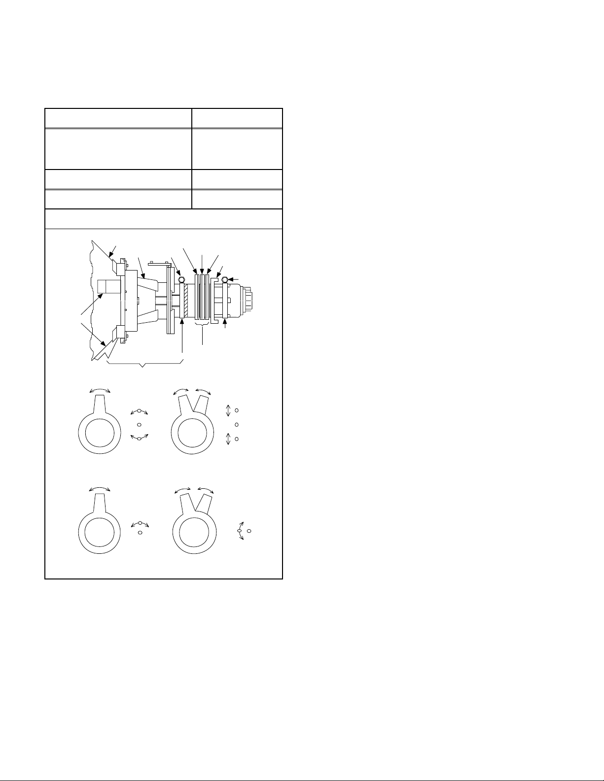
17. Convergence Adjustment
Purpose: To obtain proper convergence of red, green
and blue beams.
Symptom of Misadjustment: If Convergence Adjustment is incorrect, the edge of white letters may have
color edges.
Adj. Point Input
5. Remove the DY Wedges and slightly tilt the Deflection Yoke horizontally and vertically to obtain the
best overall convergence.
6. Fix the Deflection Yoke by carefully inserting the
DY Wedges between CRT and Deflection Yoke.
C.P. Magnet (RB),
C.P. Magnet (RB-G),
Dot Pattern or
Deflection Yoke
M. EQ. Spec.
Pattern Generator See below.
Figure
CRT
COIL
DY WEDGE
COIL CLAMPER
DEFLECTION YOKE
PURITY
SCREW
RB
C.P. MAGNET
CLAMPER
C.P. MAGNET
C.P. MAGNET (RB)
R
Crosshatch
RB-G
RING LOCK
SCREW
Fig. 6
R
G
B
G
B
Fig. 7
C.P. MAGNET (RB-G)
RB
RB
G
G
Fig. 8
1. Set the unit to the AUX Mode which is located
before CH2 then input a dot or crosshatch pattern.
2. Loosen the Ring Lock and align red with blue dots
or crosshatch at the center of the screen by rotating
(RB) C.P. Magnets. (See Fig. 7.)
3. Align red / blue with green dots at the center of the
screen by rotating (RB-G) C.P. Magnet.
(See Fig. 8.)
4. Fix the C.P. Magnets by tightening the Ring Lock.
1-9-6 TD603EA
Page 30
Adjustment Points and Test Points
Main CBA
TP1001
AGC
VR2601
+B ADJ
UPPER
FOCUS VR
LOWER
SCREEN VR
J523
+B
H.V. CBA
R583
H ADJ
VR530
H. Pincushion
Power Supply/AV CBA
J520
X-RAY
J522
X-RAY
VR531
H.SIZE
1-9-7 TD603EA
Page 31

FIRMWARE RENEWAL MODE
HOW TO UPDATE THE FIRMWARE
VERSION
1. Turn the power on and remove the disc on the tray.
2. To enter the DVD mode, press [SELECT] button on
the remote control unit. (DVD indicator lights on.)
3. To open the tray, press [OPEN/CLOSE] button on
the remote control unit.
4. To put the unit into version up mode, press [9], [8],
[7], [6], and [SEARCH MODE] buttons on the
remote control unit in that order. The tray will open
automatically.
Fig. A appears on the screen.
BE F/W VERSION UP MODE
PLEASE INSERT A DISC
FOR BE F/W VERSION UP.
The appearance shown in (*2) of Fig. B is
described as follows:
AppearanceNo. State
Reading... Sending files into the memory
1
Erasing... Erasing previous version data
2
Programming...
3 Writing new version data
7. After programming is finished, the tray opens automatically. Fig. C appears on the screen
BE F/W VERSION UP MODE
VERSION: ********
COMPLETED SUM:7abc(*3)
SELECT
EXIT:
Fig. A Version Up Mode Screen
The unit can also enter the version up mode with
the tray open. In this case, Fig. A will be shown on
the screen while the tray is open.
5. Load the disc for version up. (For closing the tray,
only the [OPEN/CLOSE] button is available.)
6. The unit enters the F/W version up mode automatically. Fig. B appears on the screen.
BE F/W VERSION UP MODE
VERSION: ********
Reading...(*2)
Fig. C Completed Program Mode Screen
At this time, no buttons are available.
8. For tray opening, plug the AC cord into the AC outlet.
9. To close the tray, press [POWER] and [SELECT]
buttons on the remote control unit or [SELECT] button on the unit.
HOW TO VERIFY THE FIRMWARE
VERSION
1. After making sure that no disc is in unit, turn the
power on.
2. Press [1], [2], [3], [4], and [DISPLAY] buttons on
the remote control unit in that order. The F/E and
B/E versions appear on the screen.
Fig. B Programming Mode Screen
1-10-1 TD603ROM
Page 32

Servo/System Control Block Diagram
SW2406 SW2408
SW2401 SW2405
FROM/TO
DVD
SYSTEM
CONTROL
BLOCK
DIAGRAM
CN401
CN2401
3 SCLK
4 CS
5 REMOTE
POWER SUPPLY / AV CBA
(DECK ASSEMBLY)
KEY SWITCH
KEY SWITCH
CN2802
6 6KEY1
5 5KEY2
CN2803
112 SDATA
12
13
15
CN1805
CN1804
11SDATA
12SCLK
13CS
15REMOTE
MAIN CBA
BLOCK DIAGRAMS <TV/VCR Section>
IC1201
(SERVO/SYSTEM CONTROL)
KEY0
5
KEY1
6
KYE2
8
SDATA
52
51
SCLK
50
CS
25
REM-OUT
REC-LED
21
DVD-H
48
TV/VCR-LED
26
REMOTE
I2C-OPEN
REC-SAFETY
C-SYNC
P-ON+5V
SW1201 SW1203,
SW1206 SW1210
KEY SWITCH
AL+5V
D1224 S-LED
D1204 REC
D1216 DVD
D1217
TV/VCR
AL+5V
Q1207
Q1211
SCL
SDA
NOTE FOR WIRE CONNECTORS:
1. PREFIX SYMBOL "CN" MEANS CONNECTOR.
(CAN DISCONNECT AND RECONNECT.)
2. PREFIX SYMBOL "CL" MEANS WIRE-SOLDER
HOLES OF THE PCB.
(WIRE IS SOLDERED DIRECTLY.)
TEST POINT INFORMATION
14
71
72
45
33
74
:INDICATES A TEST POINT WITH A JUMPER WIRE ACROSS A HOLE IN THE PCB.
:USED TO INDICATE A TEST POINT WITH A COMPONENT LEAD ON FOIL SIDE.
:USED TO INDICATE A TEST POINT WITH NO TEST PIN.
:USED TO INDICATE A TEST POINT WITH A TEST PIN.
RS1201
REMOTE
SENSOR
SW1211
REC
SAFETY
IC1202
SCL
6
5
SDA
CS
7
I2C-OPEN
C-SYNC
(MEMORY)
SCL
SDA
EXT-H
DVD-H
FROM/TO
CHROMA
/TUNER
BLOCK
DIAGRAM
AC HEAD ASSEMBLY
CONTROL
HEAD
CYLINDER ASSEMBLY
PG
SENSOR
DRUM
MOTOR
M
LOADING
MOTOR
M
CL1402
5CTL(+)
6CTL(-)
Q202
ST-SENS.
SENSOR CBA
(ST-SENSOR)
CAPSTAN MOTOR
CAPSTAN
MOTOR
M
Q201
END-SENS.
SENSOR CBA
(END-SENSOR)
P-ON+5V
C-FG
CL1201
1C-F/R
2AL+12V
3D/L+12V
4
5FG-GND
6
7C-CONT
8M-GND
9D-FG
10LD-CONT
11D-CONT
12D-PG
Q1210
WF3
CTL-AMP-OUT
SW1212
LD-SW
Q1206
T-REEL
AL+12V
D/L+12V
P-ON+5V
TP1201
Q1205
RESETT+5V
AL+5V
CTL(+)
95
94
CTL(-)
CTL AMP-OUT
97
LD-SW1
9
ST-SENS.
7
END-SENS.
T-REEL
80
RESET
34
66
C-F/R
87
C-FG
76
C-CONT
89
D-FG
82
LD-CONT
77
D-CONT
90
D-PG
DVD-MAIN-PWR
DG-ON-H
P-ON-H
P-DOWN-L
Hi-Fi-CS
Hi-Fi-DATA
Hi-Fi-CLK
ST/SAP-IN
NORMAL-H
Hi-Fi SW
DVD-MUTE
JACK-MUTE-H
A-MUTE-H
D-REC-H
VOL-CONT
V-H-SW
ENV-DET
REC/EE/PB
DV-SYNC
V-ENV
ROTA
RF-SW
TAPE-SPEED
EXT-H
RENTAL
SPL-PLAY
42
61
31
84
69
68
70
22
19
73
67
65
44
11
16
17
27
13
10
15
18
28
29
30
32
DVD-MAIN-PWR
DG-ON-H
P-ON-H
P-DOWN-L
Hi-Fi-CS
Hi-Fi-DATA
Hi-Fi-CLK
4
ST/SAP-IN
NORMAL-H
Hi-Fi SW
A-MUTE-H
DVD-MUTE
JACK-MUTE-H
A-MUTE-H
D-REC-H
VOL-CONT
EXT-H
DVD-H
V-H-SW
ENV-DET
REC/EE/PB
DV-SYNC
V-ENV
ROTA
RF-SW
TAPE-SPEED
EXT-H
RENTAL
SPL-PLAY
FROM/TO
POWER
SUPPLY BLOCK
DIAGRAM
FROM/TO
Hi-Fi AUDIO
BLOCK
DIAGRAM
FROM/TO
AUDIO BLOCK
DIAGRAM
FROM/TO
VIDEO BLOCK
DIAGRAM
1-11-1 1-11-2 TD603BLS
Page 33

Video Block Diagram
FROM/TO
CHROMA/
TUNER BLOCK
DIAGRAM
YCA-V-OUT
VIDEO
WF5
TP1402
V-OUT
IC1401
VIDEO/AUDIO
SIGNAL PROCESS
Q1401
BUFFER
35
X1401
3.58MHz
62 61
WF2
MAIN CBA
NOTE FOR WIRE CONNECTORS:
1. PREFIX SYMBOL "CN" MEANS CONNECTOR.
(CAN DISCONNECT AND RECONNECT.)
2. PREFIX SYMBOL "CL" MEANS WIRE-SOLDER
HOLES OF THE PCB.
(WIRE IS SOLDERED DIRECTLY.)
TEST POINT INFORMATION
:INDICATES A TEST POINT WITH A JUMPER WIRE ACROSS A HOLE IN THE PCB.
:USED TO INDICATE A TEST POINT WITH A COMPONENT LEAD ON FOIL SIDE.
:USED TO INDICATE A TEST POINT WITH NO TEST PIN.
:USED TO INDICATE A TEST POINT WITH A TEST PIN.
REC VIDEO SIGNAL PB VIDEO SIGNAL MODE: SP/REC
FROM
SERVO/SYSTEM
CONTROL BLOCK
DIAGRAM
EXT-H
RENTAL
REC/EE/PB
SPL-PLAY
ROTA
DV-SYNC
TAPE-SPEED
WF4
42
42
38
71
36
RENTAL
REC/EE/PB
16
SPL-PLAY
73
ROTA
14
DV-SYNC
39
TAPE-SPEED
59
V-AGC
6dB
AMP
CHARA
MIX
FBC
R P
VXO
Y/C
MIX
45 47 49 44
CCD 1H
DELAY
DOC YNR Y/C COMB
CHROMINANCE
SIGNAL PROCESS
Q1402
BUFFER
LUMINANCE
SIGNAL PROCESS
AGC
AMP
(DECK ASSEMBLY)
CYLINDER ASSEMBLY
VIDEO (R)-1 HEAD
VIDEO (L)-1 HEAD
VIDEO (L)-2 HEAD
VIDEO (R)-2 HEAD
CL1401
V(R)-1
9
V-COM
8
V(L)-1
7
V(L)-2
6
V-COM
5
V(R)-2
4
FROM/TO
SERVO/SYSTEM
CONTROL BLOCK
DIAGRAM
WF1
RF-SW
V-ENV
V-H-SW
ENV-DET
TP1401
RF-SW
91
90
89
88
85
84
83
82
13
93
15
94
ENV-DET
R
L
SP
EP
L
R
HPF
ENV
DET
R
P
74
TP1403
ENV
WF6
1-11-3 1-11-4 TD603BLV
Page 34

Audio Block Diagram
NOTE FOR WIRE CONNECTORS:
1. PREFIX SYMBOL "CN" MEANS CONNECTOR.
(CAN DISCONNECT AND RECONNECT.)
2. PREFIX SYMBOL "CL" MEANS WIRE-SOLDER
HOLES OF THE PCB.
(WIRE IS SOLDERED DIRECTLY.)
TEST POINT INFORMATION
:INDICATES A TEST POINT WITH A JUMPER WIRE ACROSS A HOLE IN THE PCB.
:USED TO INDICATE A TEST POINT WITH A COMPONENT LEAD ON FOIL SIDE.
:USED TO INDICATE A TEST POINT WITH NO TEST PIN.
:USED TO INDICATE A TEST POINT WITH A TEST PIN.
CN2402
FROM DVD AUDIO
BLOCK DIAGRAM
CN402
FROM
Hi-Fi AUDIO
BLOCK
DIAGRAM
FROM
SERVO/
SYSTEM
CONTROL
BLOCK DIAGRAM
CN1804
A-OUT(R)5 5
A-OUT(L)3 3
DVD-H19 19
SPDIF11
DVD-AUDIO(R)
7
DVD-AUDIO(L)
5
DVD-MUTE13
CN2803
CN2803CN1804
IC2203
(OP AMP)
5
3 1
Q2207
7
Q2205
BUFFER
IC2202
(OUTPUT SELECT)
2
1
12
13
SW CTL.
1110
Q2203
15
14
Q2209
P-ON+5V
REC-AUDIO SIGNAL
IC2801
(AUDIO AMP)
5
2 12
DC VOL.
6
Q2204
Q2202
Q2208
VOLUME
JACK-MUTE-H
DVD-MUTE
PB-AUDIO SIGNAL
POWER SUPPLY / AV CBA
7
JK2201
DIGITAL
A-OUT
A-OUT(R)
A-OUT(L)
FROM/TO
SERVO/SYSTEM
CONTROL BLOCK
DIAGRAM
CN2801
SP-L
SP-GND 2
DVD AUDIO SIGNAL DATA(AUDIO) SIGNAL
CN1805CN2802
A-OUT(R)10 10
A-OUT(L)9 9
SP-L11 11
1
SP2801
SPEAKER
L-CH
CN1802
SP-R
SP-GND 2
Mode : SP/REC
1
SP1801
SPEAKER
R-CH
JK1801
HEADPHONE
JACK
FROM/TO
Hi-Fi AUDIO
BLOCK
DIAGRAM
N-A-IN
N-A-OUT
BLOCK DIAGRAM FOR SECTION 2 (DECK MECHANISM)
AC HEAD ASSEMBLY
AUDIO
HEAD
AUDIO
ERASE
HEAD
FE HEAD UNIT
FULL
ERASE
HEAD
CL1402
A-PB/REC
4
A-COM
3
AE-H
1
AE-H/FE-H
2
CN1403
FE-H
1
FE-H GND
2
Q1873
Q1874
Q1872
BIAS
OSC
Q1875
Q1871
P-ON+5V
P-ON+5V
76
78
80
4
99
IC1401
(AUDIO PROCESS)
EQ
AMP
3
AUTO
BIAS
SP/LP-ON
ALC
REC
AMP
LINE
AMP
11
EXT-H
96
98
FROM SERVO/SYSTEM
CONTROL BLOCK
DIAGRAM
MUTE
D-REC-H
EXT-H
7112
A-MUTE-H
D-REC-H
R
1
2
6
100
P
7
WF8
WF7
TP1802
NA-IN-YCA
1-11-5
MAIN CBA
TD603BLA1-11-6
Page 35

Hi-Fi Audio Block Diagram
FROM
CHROM/TUNER
BLOCK DIAGRAM
SIF
NOTE FOR WIRE CONNECTORS:
1. PREFIX SYMBOL "CN" MEANS CONNECTOR.
(CAN DISCONNECT AND RECONNECT.)
2. PREFIX SYMBOL "CL" MEANS WIRE-SOLDER
HOLES OF THE PCB.
(WIRE IS SOLDERED DIRECTLY.)
IC1751(MTS/ SAP/ Hi-Fi AUDIO PROCESS/ Hi-Fi HEAD AMP)
NOISE
DET
57
SIF
DEMOD
SAP
FILTER
STEREO
FILTER
PILOT
DET
TEST POINT INFORMATION
SAP
DEMOD
PILOT
CANCEL
:INDICATES A TEST POINT WITH A JUMPER WIRE ACROSS A HOLE IN THE PCB.
:USED TO INDICATE A TEST POINT WITH A COMPONENT LEAD ON FOIL SIDE.
:USED TO INDICATE A TEST POINT WITH NO TEST PIN.
:USED TO INDICATE A TEST POINT WITH A TEST PIN.
L-R
DEMOD
MAIN CBA
ST/SAP
SW
DC
dBX
DEC
MATRIX
SERIAL
DATA
DECODER
RIPPLE
FILTER
37
38
39
54
REC-AUDIO SIGNALPB-AUDIO SIGNAL Mode : SP/REC
Hi-Fi-CS
Hi-Fi-DATA
Hi-Fi-CLK
P-ON+9V
FROM SERVO/ SYSTEM
CONTROL BLOCK
DIAGRAM
JK1703
A-IN(R)
JK1702
A-IN(L)
TO AUDIO
BLOCK
DIAGRAM
N-A-OUT
69
STEREO
PLL
R-CH
INSEL
6
NOR
SW
48 47
R-CH
PNR
P
R
SW
NOISE
LIM DEV
COMP
VCO
HOLD
PULSE
NOISE
DET
LPF
MATRIX
R-CH BPF
OUTPUT
SELECT
BO
DET
COMP
ENV
DET
MODE OUT
51
23
80
78
77
40
49
26
ST/SAP-IN
NORMAL-H
4
TP1701
Hi-Fi-OUT-L
TP1702
Hi-Fi-OUT-R
1
N-A-IN
A-OUT(L)
A-OUT(R)
Hi-Fi-SW
A-MUTE-H
TO SERVO/SYSTEM
CONTROL BLOCK
DIAGRAM
FROM/TO
AUDIO BLOCK
DIAGRAM
FROM
SERVO/SYSTEM
CONTROL BLOCK
DIAGRAM
CYLINDER
LIM DEV
7
L-CH
INSEL
13 14
L-CH
PNR
R
SW
P
NOISE
VCO
COMP
LPF
L-CH BPF
AGC
AGC
DET
31 30
R
L
24
27
CL1701A CL1701B
1
2
3
CL1701
1
2
3
CL1401
Hi-Fi-A(R) 3
Hi-Fi-COM 2
Hi-Fi-A(L) 1
ASSEMBLY
Hi-Fi
AUDIO
(R) HEAD
Hi-Fi
AUDIO
(L) HEAD
TD603BLH1-11-7 1-11-8
Page 36

Chroma/Tuner Block Diagram
NOTE FOR WIRE CONNECTORS:
1. PREFIX SYMBOL "CN" MEANS CONNECTOR.
(CAN DISCONNECT AND RECONNECT.)
2. PREFIX SYMBOL "CL" MEANS WIRE-SOLDER
HOLES OF THE PCB.
(WIRE IS SOLDERED DIRECTLY.)
MAIN CBA
TP1001
AGC
TU1001
AGC
1
IF
11
SDA
5
SCL
4
FSC
8
CN1303(NO CONNECTION)
INT.MONITOR
I2C-OPEN
CN1303 is used for
adjustment at factory
FROM/TO
SERVO/SYSTEM
CONTROL
BLOCK DIAGRAM
1
2
SDA 4
SCL 5
SCL
SDA
I2C-OPEN
C-SYNC
TEST POINT INFORMATION
SF1001
SAW
FILTER
:INDICATES A TEST POINT WITH A JUMPER WIRE ACROSS A HOLE IN THE PCB.
:USED TO INDICATE A TEST POINT WITH A COMPONENT LEAD ON FOIL SIDE.
:USED TO INDICATE A TEST POINT WITH NO TEST PIN.
:USED TO INDICATE A TEST POINT WITH A TEST PIN.
IC1301(VIDEO/AUDIO/CHROMA/DEFLECTION/IF)
REC VIDEO SIGNAL PB VIDEO SIGNAL
59
63
IF SIGNAL
CONTROL
64
CIRCUIT
43
26
SERIAL
I/F
27
INTELLIGENT
18
MONITORING
SYNC
SEPARATION
CHROMA
TRAP
CHROMA
BPF
CLOCK
CONTROL
CIRCUIT
29FSC-OUT
58
41
38
34
4
14
15
X1301
3.58MHz
DVD VIDEO SIGNAL
IC1501 (Y/C SEPARATION)
9
BUS
I/F
10
IC1601
(INPUT SELECT)
TUNER
LINE
SW CTL
Q1601
VCR
DVD
11109
VCR
DVD
13
Q1503
BUFFER
3
5
13
12
1
2
REC-AUDIO SIGNAL
Y/C
SEPA.
1720
BUFFER
CN1803
14 14
4
CY
Q1504
CF1302
4.5MHz
BPF
CF1301
4.5MHz
TRAP
DVD-Y
DVD-C13 13
Q1501,
Q1502
BUFFER
Q1603
BUFFER
CN2804
BUFFER
BUFFER
BUFFER
BUFFER
Q2210
Q2211
Mode : SP/REC
YCA-V-OUT
Q1302
Q1301
CN2402
TP2201
DVD-V
VIDEO
SIF
DVD-Y14
DVD-C18
DVD-VIDEO16
FROM/TO VIDEO
BLOCK DIAGRAM
TO Hi-Fi AUDIO
BLOCK DIAGRAM
JK1701
V-IN
FROM
DVD VIDEO
BLOCK
DIAGRAM
CN402
IC1201
(SYSTEM CONTROL/OSD)
OSD-R
OSD-G
OSD-B
OSD-BLK
WF18
V-SYNC
WF17
H-SYNC
64
63
62
60
59
58
WF9
23
22
21
24
20
19
V-SYNC
PROCESS
CIRCUIT
H-SYNC
PROCESS
CIRCUIT
LUMA
SIGNAL
PROCESS
CIRCUIT
CHROMA
SIGNAL
PROCESS
CIRCUIT
OSD MIX/RBG MATRIX/
BLANKING
14
15
16
11
10
33
5
6
Q1602
DVD-H
EXT-H
CN1301
WF10
CN1302
RED4
GREEN3
BLUE
2
7
V-DRIVE
3
H-DRIVE
2
FBP-IN
6
ACL/ABL
4
V-RAMP-NF
FROM SERVO/SYSTEM
CONTROL
BLOCK DIAGRAM
TO
CRT/H.V. BLOCK DIAGRAM
CN504
FROM/TO
CRT/H.V. BLOCK DIAGRAM
CN503
POWER SUPPLY
/ AV CBA
TD603BLC1-11-9 1-11-10
Page 37

CRT/H.V. Block Diagram
TEST POINT INFORMATION
:INDICATES A TEST POINT WITH A JUMPER WIRE ACROSS A HOLE IN THE PCB.
:USED TO INDICATE A TEST POINT WITH A COMPONENT LEAD ON FOIL SIDE.
:USED TO INDICATE A TEST POINT WITH NO TEST PIN.
:USED TO INDICATE A TEST POINT WITH A TEST PIN.
NOTE FOR WIRE CONNECTORS:
1. PREFIX SYMBOL "CN" MEANS CONNECTOR.
(CAN DISCONNECT AND RECONNECT.)
2. PREFIX SYMBOL "CL" MEANS WIRE-SOLDER
HOLES OF THE PCB.
(WIRE IS SOLDERED DIRECTLY.)
FROM
POWER SUPPLY
BLOCK DIAGRAM
CN2602
CN502
1 +B
2 +B
4 DEF+B
CL502B
JUNCTION B
CBA
1
2
4
CL502A
+B1
2 +B
4 DEF+B
Q591
H.DRIVE
WF11
Q571
H.OUTPUT
J523
+B
J516
GND
T572
1
REC VIDEO SIGNAL PB VIDEO SIGNAL
IC551 (V-DEFLECTION CONTROL)
7
AMP
1
6
T571 F.B.T.
HV
F
S
11
THERMAL
PROTECTION
PULSE
UP
3
FOCUS VR
5
Q532
Q530,
Q531
ANODE
H.
CONTROL
PINC. WIDTH
DVD VIDEO SIGNAL
WF12
5
4
3
VR531VR530
1
CN571
L551
D.Y.
VDRIVE
HDRIVE
FROM/TO
CHROMA/TUNER
BLOCK DIAGRAM
CN1302
FROM
CHROMA/TUNER
BLOCK DIAGRAM
CN1301
CN503
7
V-DRIVE
3
H-DRIVE
2
FBP-IN
6
ACL/ABL
4
V-RAMP-NF
CN504 CL504B
4
RED
3
GREEN
2
BLUE
CL503B
3
5
4
CL503A
7
7
3
2
6
4
4
3
2
V-DRIVE
3
H-DRIVE
2
FBP-IN
6
ACL/ABL
4
V-RAMP-NF
CL504A
4 RED
3
GREEN
2
BLUE
Q503
RED AMP
8
10
7
9
6
H.V. CBA
SCREEN VR
Q502
GREEN AMP
FOCUS
SCREEN
ANODE
CL501CL501A
HEATER 11
P-ON+180V 33
JK501
FOCUS
WF14WF13
BLUE AMP
Q501
WF15
CN501
SCREEN
GND
R
G
B
HEATER
GND
V501
CRT
JUNCTION A
CBA
CRT CBA
1-11-121-11-11
TD603BLCRT
Page 38

Power Supply Block Diagram
CAUTION !
Fixed voltage power supply circuit is used in this unit.
If Main Fuse (F2601) is blown, check to see that all components in the power supply
circuit are not defective before you connect the AC plug to the AC power supply.
Otherwise it may cause some components in the power supply circuit to fail.
4A/125V
W2601
DEGAUSSING
COIL
F2601
4A/125V
CN2601
LINE
FILTER
PS2601
L2601
D2603 D2606
BRIDGE
RECTIFIER
Q2601
SWITCHING
Q2602
4A/125V
T2601
6
4
2
1
IC2611
ERROR
VOLTAGE DET
4
CAUTION
FOR CONTINUED PROTECTION AGAINST FIRE HAZARD,
REPLACE ONLY WITH THE SAME TYPE FUSE.
ATTENTION : POUR UNE PROTECTION CONTINUE LES RISQES
D'INCELE N'UTILISER QUE DES FUSIBLE DE MEMO TYPE.
RISK OF FIRE-REPLACE FUSE AS MARKED.
"This symbol means fast operating fuse."
"Ce symbole reprèsente un fusible à fusion rapide."
14
Q2606
13
12
11
10
9
8
Q2607
VR2601
+B ADJ
1
Q2604
23
FEED
BACK
Q2613
Q2608
Q2605
NOTE :
The voltage for parts in hot circuit is measured using
hot GND as a common terminal.
NOTE FOR WIRE CONNECTORS:
1. PREFIX SYMBOL "CN" MEANS CONNECTOR.
(CAN DISCONNECT AND RECONNECT.)
2. PREFIX SYMBOL "CL" MEANS WIRE-SOLDER
HOLES OF THE PCB.
(WIRE IS SOLDERED DIRECTLY.)
IC1602
CN2602 TO CN502
1 +B
2 +B
4 DEF+B
CN2804 CN1803
6 6P-ON+9V
8 8AL+9V
3 3AL+33V
4 4P-ON+9V
16 16AL+12V
10 10AC-DOWN
19 19P-ON+5V
7 7DG-ON-H
TO CRT/H.V.
BLOCK DIAGRAM
+5V REG.
Q1608
SW+5V
Q1611
SW+5V
Q1613
SW+5V
Q1609
+5V REG.
MAIN CBA
CN2803 CN1804
17 17P-ON-H
16 16
DVD-MAIN-PWR
P-ON+5V
P-ON+5V
P-ON+5V
P-ON+5V
T+5V
AL+33V
P-ON+9V
AL+12V
AL+5V
Q1612
P-DOWN-L
(TO PIN84 OF IC1201)
+5V CTRL
(FROM PIN49 OF IC1301)
P-ON-H
(FROM PIN31 OF IC1201)
DVD-MAIN-PWR
(FROM PIN42 OF IC1201)
DG-ON
(FROM PIN61 OF IC1201)
HOT
RL2601
Q2603
(SWITCHING)
COLD
IC2615
1 2
Q2615
Q2610
Q2612
+4V
REG.
5
Q2616
IC2616
IC2617
+1.8V
1 2
REG.
4
Q2611
POWER SUPPLY/AV CBA
Q2614
SW
CTL.
Q2617
CN2402 CN402 CN701
9 9DVD-ON+5V
3 3EV+3.3V
2 2EV+2.5V
1 1EV+2.5V
CN401CN2401
16 16DVD-ON+5V
18 18DVD-ON+1.8V
17 17DVD-ON+1.8V
9 9DVD-ON+3.3V
8 8DVD-ON+3.3V
7 7DVD-ON+3.3V
11 11EV+9V
10 10EV+9V
6 6PWRCON
CN404
2 13DVD-ON+5V
CN404
11 16EV+3.3V
23 4EV+2.5V
24 3EV+2.5V
21 6DVD-ON+5V
22 5DVD-ON+5V
25 2DVD-ON+1.8V
26 1DVD-ON+1.8V
8 19DVD-ON+3.3V
9 18DVD-ON+3.3V
10 17DVD-ON+3.3V
12 15EV+9V
13 14EV+9V
CN501
FILTER CBA
CN2401
6 PWRCON
FROM DVD SYSTSM
CONTROL BLOCK
DIAGRAM CN401
DVD MAIN
CBA UNIT
DVD-ON+5V
EV+3.3V
EV+2.5V
DVD-ON+5V
DVD-ON+1.8V
DVD-ON+3.3V
AL+9V
1-11-141-11-13
TD603BLP
Page 39

DVD System Control Block Diagram
FROM/TO
RF SIGNAL
PROCESS
/SERVO
BLOCK
DIAGRAM
TFWD
TREV
TIN
TOUT
SCK
STDIO
SEN
MUTE
PS
42
41
59
60
70
72
10
46 MUTE
47 PS
" " = SMD
IC301
(FRONT END PROCESSOR)
TFWD
TREV
TIN
TOUT
SCK
STDIO
SEN
HANG
+3.3V
48
BLOCK DIAGRAMS<DVD Section>
NOTE FOR WIRE CONNECTORS:
1. PREFIX SYMBOL "CN" MEANS CONNECTOR.
(CAN DISCONNECT AND RECONNECT.)
2. PREFIX SYMBOL "CL" MEANS WIRE-SOLDER
HOLES OF THE PCB.
(WIRE IS SOLDERED DIRECTLY.)
IC601
(DVD HOST PROCESSOR)
TFWD
200
TREV
201
187
TIN
TOUT
188
IC605
RESET
RESET
5 4
Q701
124
FROM/TO
DVD SIGNAL
PROCESS
BLOCK
DIAGRAM
CD/DVD
CFE
CAS
STANDBY
ADDRESS BUS
DATA BUS
NINT1
NINT2
WAIT
/RE
/WEL
CS1
RESET
CD/DVD
71
CFE
62
CAS
63
STANDBY
64
13
~
16
26
CPUADR0
33
CPUADR17
35
40
CPUDT0
84
~ ~~
91
CPUDT7
76
NINT1
77
NINT2
WAIT
1
/RE
2
/WEL
3
CS1
6
RESET
11
READY
OSCO2324
~
~
KEY OUT
KEY IN
49
82
/FERS
OSCI
X301
(16.9344MHz)
53 22BUSCLR BUSCLR
52
SDA
51
SDA
50
SCL
79SCL
44
45
IC606
(INVERTER)
2 4
X601 27MHz
+3.3V
208
186
120
20
21
127
READY
/FERS
CLOCK
SDA
SCL
IRQ2
VFD-CLK
REMOTE
PWRCON
3VFD-STB
1VFD-DIN
204
125
207
CN501 CN403
CS
21
SDATA
22
SCLK
24
REMOTE
26
PWRCON
7
6
5
3
1
7
FILTER CBA
CN401
CS 4
SDATA 2
SCLK 3
REMOTE 5
PWRCON 6
FROM/TO
SERVO/SYSTEM
CONTROL BLOCK
DIAGRAM CN2401
TO POWER SUPPLY
BLOCK DIAGRAM
CN2401
FG
SENSOR
FG CBA
RELAY
CBA
CN401
FG-IN10
1-11-15
FG-IN
IC102 (OP AMP)
1480
12
DVD MAIN CBA UNIT
1-11-16
TD603BLDS
Page 40

RF Signal Process/Servo Block Diagram
NOTE FOR WIRE CONNECTORS:
1. PREFIX SYMBOL "CN" MEANS CONNECTOR.
" " = SMD
(CAN DISCONNECT AND RECONNECT.)
2. PREFIX SYMBOL "CL" MEANS WIRE-SOLDER
HOLES OF THE PCB.
(WIRE IS SOLDERED DIRECTLY.)
DATA(VIDEO/AUDIO) SIGNAL FOCUS SERVO SIGNAL TRACKING SERVO SIGNAL
SLIDE SERVO SIGNAL DISK SERVO SIGNAL
PICK-UP UNIT
DETECTOR
A 6
B 9
C 10
D 7
F 4
E 5
CD/DVD 21
CD-LD 20
DVD-LD 12
PD-MONI 11
GND 14
GND 13
GND 19
CN101
CN101
IC103
(SW)
AMP
Q102
1 3
AMP
Q101
IC101 (RF SIGNAL PROCESS)
HOLD
47
57
58
59
60
62
63
4
2
3
1
6
INPUT
MATRIX
TRACKING
BALANCE
FOCUS
BALANCE
LPC
AMP
VGA
EQ
TRACKING
ERROR DET
FOCUS
ERROR DET
VEL
ADJ
BDO DET
OFTR DET
MIRROR DET
SERIAL
I/F
41
46
31
30
40
39
18
6
22
7
20
11
13
14
12
DVD MAIN CBA UNIT
TESTSG
ARF
NARF
STANDBY
SCK
STDIO
SEN
CD/DVD
FROM/TO DVD
SIGNAL PROCESS
BLOCK DIAGRAM
LOADING
MOTOR
SPINDLE
MOTOR
SLIDE
MOTOR
FSTS
CN101
FS(+) 17
FS(-) 16
TS(+) 15
TS(-) 18
RELAY CBA
M
M
M
TRAY
-IN
TRAY-OUT
TRAY-IN 3
TRAY-OUT 4
CN401
LM(+) 1
LM(-) 2
SP(-) 6
SP(+) 7
SL(+) 9
SL(-) 8
GND 5
4
+3.3V
IC401
(SERVO DRIVE)
12 6
11
14
13
10
9
18
17
15
16
FOCUS
MOTOR DRIVE
TRACKING
MOTOR DRIVE
MUTE
LOADING
MOTOR DRIVE
SPINDLE
MOTOR DRIVE
SLIDE
MOTOR DRIVE
+
-
+
-
POWER
SAVE
21
24
23
22
27
26
25
5
1
2
V-REF
4
IC201 (SERVO DSP)
DAC1
115
DAC0
114
68
SPDRV
67
TRSDRV
FBAL
TBAL
OFTR
BDO
AD1
AD0
TRCRS
AD2
AD3
66
65
51
52
118
117
90
119
120
IC102
(OP AMP)
5
3
FROM/TO DVD
SYSTEM CONTROL
BLOCK DIAGRAM
CFE
7
108
CAS
1
MUTE
TFWD
TREV
TIN
PS
TOUT
SW CBA
1-11-18
TD603BLRF1-11-17
Page 41

DVD Signal Process Block Diagram
IC201 (DVD SIGNAL PROCESS)
FROM/TO RF SIGNAL
PROCESS/SERVO
BLOCK DIAGRAM
ARF
NARF
TESTSG
111
110
82
" " = SMD
PLL
VCO
DATA
SLICER
BCA
DVD
DEMODULATOR
DATA(VIDEO/AUDIO) SIGNAL
VIDEO/AUDIO
INTERFACE
PARA0
PARA1
PARA2
PARA3
PARA4
PARA5
PARA6
PARA7
172
168
166
164
160
158
151
149
DVD MAIN CBA UNIT
PARA0-PARA7
TO DVD VIDEO
BLOCK DIAGRAM
FROM/TO DVD
SYSTEM CONTROL
BLOCK DIAGRAM
ADDRESS BUS
DATA BUS
NINT1
NINT2
WAIT
/RE
/WEL
CS1
RESET
X201
(16.9344MHz)
30
~
CPUADR0
22
17
CPUADR17
9
CPUDT0
44
~ ~
37
CPUDT7
2
NINT1
5
NINT2
WAIT
6
/RE
36
/WEL
35
CS1
34
RESET
47
OSCI1
79
OSCO1
80
MEMORY
MANAGER
~
~
CPU
INTERFACE
TD603BLD1-11-19 1-11-20
Page 42

DVD Video Block Diagram
DATA(VIDEO) SIGNAL DVD VIDEO SIGNALDATA(AUDIO) SIGNAL
IC601 (DVD HOST PROCESSOR)
" " = SMD
DATA(VIDEO/AUDIO) SIGNAL
NOTE FOR WIRE CONNECTORS:
1. PREFIX SYMBOL "CN" MEANS CONNECTOR.
(CAN DISCONNECT AND RECONNECT.)
2. PREFIX SYMBOL "CL" MEANS WIRE-SOLDER
HOLES OF THE PCB.
(WIRE IS SOLDERED DIRECTLY.)
FROM DVD
SIGNAL PROCESS
BLOCK DIAGRAM
TO DVD AUDIO
BLOCK DIAGRAM
IC602
(8Mbit FLASH MEMORY)
25
A0
16
~
8
A18
1
48
DQ0
29
~
DQ15
45
11
WE
26
CE
28
OE
PARA0-PARA7
A-MUTE
ADAC-MD
ADAC-MC
ADAC-ML
~
ADDR1-ADDR20
~
DATA0-DATA15
~
PARA0
6
~
PARA7
13
191
A-MUTE
190
ADAC-MD
189
ADAC-MC
ADAC-ML
192
161
~
170
ADDR1
173
ADDR20
~
182
DATA0
141
~
DATA15
158
DQM0
128
CS3
132
OE
117
CPU
INTERNAL
~
PERIPHERALS
PORTS
~
PROGRAMMABLE
CPU INTERFACE
SHARED SDRAM INTERFACE
CENTRAL
COMMAND
PORT
ST20 ARBITER &
MEMORY CONTROLLER
I/F
VIDEO
DECODER
CD FIFO
SDRAM ARBITER
VIDEO
FILTERING
CACHE
SUBSYSTEM
FRONT-END
& LINK
INTERFACE
SDRAM
BLOCK
MOVE
OSD, SP
DECODER
& MIXING
AUDIO
DECODER
DENC
51
52
55
56
57
32
33
34
PCM-BCK
PCM-DATA0
PCM-SCLK
PCM-LRCLK
SPDIF
TO DVD AUDIO
BLOCK DIAGRAM
CN701
5 14DVD-Y
9 10DVD-C
7 12
DVD-VIDEO
CN404
CN402
14DVD-Y
TO CHROMA/TUNER
18DVD-C
BLOCK DIAGRAM
CN2402
16DVD-VIDEO
~
~
AD0
AD13
58 63~66 73~ 74
~
DQML
DQMU
79 80 78
WE
CS
RAS
102
CAS
7677
DQ0
DQ15
97
~84 93~
AD0-AD13
20 26~ 2 13~29 35~ 42 53~
~
AD0
AD13
DQ0-DQ15
~
DQ0
IC604
(64Mbit SDRAM)
17 18 39 16
DQ15
FILTER CBA
15
RAS
CAS
19
CS
WE
LDQM
UDQM
DVD MAIN CBA UNIT
1-11-22
TD603BLDV1-11-21
Page 43

DVD Audio Block Diagram
" " = SMD
NOTE FOR WIRE CONNECTORS:
1. PREFIX SYMBOL "CN" MEANS CONNECTOR.
(CAN DISCONNECT AND RECONNECT.)
2. PREFIX SYMBOL "CL" MEANS WIRE-SOLDER
HOLES OF THE PCB.
(WIRE IS SOLDERED DIRECTLY.)
DVD AUDIO SIGNALDATA(AUDIO) SIGNAL
TEST POINT INFORMATION
:INDICATES A TEST POINT WITH A JUMPER WIRE ACROSS A HOLE IN THE PCB.
:USED TO INDICATE A TEST POINT WITH A COMPONENT LEAD ON FOIL SIDE.
:USED TO INDICATE A TEST POINT WITH NO TEST PIN.
:USED TO INDICATE A TEST POINT WITH A TEST PIN.
FROM
DVD VIDEO
BLOCK DIAGRAM
SPDIF
PCM-BCK
PCM-DATA0
PCM-LRCLK
ADAC-MD
ADAC-MC
ADAC-ML
IC801 (AUDIO DAC)
1
2
3
13
14
15
SERIAL
PORT
SERIAL
CONTROL
4X/8X
OVERSAMPLING
DIGITAL FILTER
/FUNCTION
CONTROLLER
ENPHANCED
MULTI-LEVEL
DELTA-SIGMA
MODULATOR
ZERO DETECT
SYSTEM CLOCK
DAC LPF+AMP
DAC
LPF+AMP
L-CH
R-CH
12
11
CN701
181SPDIF
13 6
DVD AUDIO(L)
154DVD AUDIO(R)
12 7A-MUTE(L)
14 5A-MUTE(R)
16 3A-MUTE
7
8
CN404
CN402
11 SPDIF
5 DVD-AUDIO(L)
7 DVD-AUDIO(R)
13 DVD-MUTE
TO AUDIO BLOCK
DIAGRAM CN2402
FILTER CBA
PCM-SCLK
A-MUTE
16
DVD MAIN CBA UNIT
TD603BLDA1-11-23 1-11-24
Page 44

SCHEMATIC DIAGRAMS / CBA’S AND TEST POINTS
Standard Notes
WARNING
Critical components having special safety characteristics are identified with a # by the Ref. No. in the parts
list and enclosed within a broken line* (where several
critical components are grouped in one area) along
with the safety symbol # on the schematics or
exploded views.
Use of substitute replacement parts which do not have
the same specified safety characteristics may create
shock, fire or other hazards.
Under no circumstances should the original design be
modified or altered without written permission from
Philips Consumer Electronics Company. Philips
assumes no liability, express or implied, arising out of
any unauthorized modification of design. Servicer
assumes all liability.
* Broken Line :
Capacitor Temperature Markings
Mark
(B)
Capacity
change rate
±10%
(F) +30 - 80% 20°C –25~+85°C
(SR)
(Z)
±15%
±22.5%
Capacitors and transistors are represented by the following symbols.
< PCB Symbols >
(Top View) (Bottom View)
(Bottom View)
E C B
(Top View)
E C B
(Top View)
E C B
+
Transistor or Digital Transistor
NPN Transistor
NPN Digital Transistor
Standard
temperature
20°C -25~+85°C
20°C –25~+85°C
20°C –25~+85°C
Electrolytic Capacitor
(Top View)
E C B
(Top View)
E C B
Temperature
range
PNP Transistor
PNP Digital
Transistor
Notes:
1. Do not use the part number shown on these drawings for ordering. The correct part number is shown
in the parts list, and may be slightly different or
amended since these drawings were prepared.
2. To maintain original function and reliability of
repaired units, use only original replacement parts
which are listed with their part numbers in the parts
list section of the service manual.
3. Prefix symbol "CN" means "connector" (can disconnect and reconnect).
Prefix symbol "CL" means "wire-solder holes of the
PCB" (wire is soldered directly).
4. How to read converged lines.
1-D3
Distinction Area
Line Number
(1 to 3 digits)
Examples:
(1). "1-D3" means that line number "1" goes to area
"D3."
(2). "1-B1" means that line number "1" goes to area
"B1."
5. All resistance values are indicated in ohms
3
(K=10
, M=106).
6. Resistor wattages are 1/4W or 1/6W unless otherwise specified.
7. All capacitance values are indicated in µF
-6
(P=10
µF).
8. All voltages are DC voltages unless otherwise
specified.
9. Voltage indications for PLAY and REC modes on
the schematics are as shown below
1
(Unit: Volt)
The same voltage for
both PLAY & REC modes.
5.0
< Schematic Diagram Symbols >
Digital Transistor
3
AREA D3
2
1
2
3
5.0
(2.5)
Indicates that the voltage
is not consistent here.
AREA B1
1-D3
ABCD
PLAY mode
REC mode
1-B1
1-12-1 SC_5
Page 45

Main 1/4 Schematic Diagram Parts Location Guide < TV/VCR Section >
A-5
A-5
A-5
SWITCHES
TEST PO IN TS
Ref No. Position Ref No. Position Ref No. Position Ref No. Position Ref No. Posit ion
CAPACITORS
C1203 B -4 C1635 B-1 IC1602 B-2 R1226 A-4 R1293 E-4
C1204 B -4 C1636 C-1 R1227 B -4 R1294 E - 3
C1205 B -4 L1201 D-2 R1228 B-3 R1295 E -4
C1207 A -4 CL1201 A-3 L1202 F-3 R1229 B-4 R1296 D-5
C1208 E -2 CN1802 G-1 L1203 D-1 R1230 B-4 R1297 D-3
C1209 D-2 CN1803 A-2 L1211 A-3 R1231 B-4 R1299 F-4
C1210 D-2 CN1804 G-3 L1802 F-1 R1233 E-2 R1646 B-2
C1211 D-2 CN1805 G-2 L1803 F-1 R1234 E-2 R1647 B-2
C1212 C-2 L1804 F-1 R1235 D-2 R1648 B-1
C1213 C-2 D1201 B-4 L1806 G-1 R1236 D-2 R1650 B-1
C1214 D-2 D1202 B-4 L1807 G-1 R1237 D-2 R1651 B-1
C1216 D-2 D1203 C-5 R1238 C-3 R1652 B-1
C1217 D-2 D1204 B-4 Q1205 D-2 R1239 D-3 R1653 B-1
C1218 D-2 D1205 B-4 Q1206 E-5 R1240 D-3 R1656 B-1
C1219 E -3 D1206 B-4 Q1207 B-3 R1241 D-2 R1657 A-1
C1220 E -3 D1207 D-2 Q1210 B-3 R1243 E-3 R1659 B-1
C1221 F-3 D1208 D-2 Q1211 B-3 R1244 E- 3 R1660 B -1
C1222 E -3 D1209 E-3 Q1608 B-1 R1245 E-3 R1661 B -1
C1223 E -3 D1210 E-3 Q1609 B-1 R1247 E-4 R1801 F-1
C1224 E -3 D1211 F-3 Q1611 B-1 R1248 E -3 R1802 F-1
C1225 E -3 D1212 F-5 Q1612 C-1 R1249 E-4 R1980 B-4
C1231 F-4 D1213 E-5 Q1613 B-1 R1250 E- 4 R1981 A -3
C1232 F-4 D1214 C-5 R1251 E-4 R1990 E -4
C1233 E -5 D1215 C-5 R1200 E-4 R1252 E-4
C1235 F-5 D1216 B-3 R1201 B -5 R1253 E- 4 S W 1201
C1238 A -3 D1217 B - 3 R1202 B- 5 R1254 F-4 SW1202 A-5
C1239 D-5 D1219 E-2 R1203 B-5 R1255 E- 4 S W1203
C1240 D-5 D1220 F-3 R1204 B-5 R1256 F-5 SW1206
C1241 D-5 D1221 F-3 R1205 B-5 R1257 F-5 SW1207 A-5
C1243 C-5 D1222 F-4 R1206 B-5 R1258 E-4 SW1208 A-5
C1244 C-5 D1223 F-5 R1207 B-5 R1259 F-5 SW1209 A-5
C1245 C-5 D1224 B-4 R1208 B-4 R1260 F-5 SW1210 A-5
C1246 C-5 D1225 E-5 R1209 C-5 R1263 E-4 SW1211 C-3
C1247 C-5 D1631 B-1 R1210 B-5 R1264 E- 5 S W1212 B-5
C1249 C-5 D1632 C-1 R1211 B-5 R1266 E-5
C1250 C-2 D1633 C-1 R1212 B-5 R1267 E-5 X1201 C-3
C1252 A -4 D1634 C-2 R1213 B-4 R1268 E-4 X1202 D-3
C1253 A -3 D1635 C-2 R1214 B-5 R1269 D-5
C1254 A -3 D1637 B-2 R1215 B-5 R1270 D-5 JK1801 G-1
C1255 D-5 D1638 B-2 R1216 B-5 R1271 B- 3 RS1201 A-4
C1257 F-1 D1639 B-2 R1217 B -5 R1272 D-5
C1258 E -4 D1640 C-2 R1218 B-5 R1273 D-5 TP1201 C-5
C1259 C-3 D1806 F-1 R1219 C-4 R1274 D-5 TP1631 C-2
C1260 A -3 D1807 F-1 R1220 B-4 R1275 D-3 TP1632 C-2
C1628 B -1 D1964 B - 4 R1221 C-4 R1278 B-3
C1629 B -1 D1965 B - 4 R1222 B- 4 R1280 C-5
C1630 B -1 R1223 C-4 R1290 E-3
C1631 C-1 IC1201 D-4 R1224 B-3 R1291 E -3
C1634 B -1 IC1202 F-5 R1225 A-4 R1292 E-3
CONNECTORS
DIODES
ICS
ICSCAPACITORS
COILS
TRANSISTORS
RESISTORS
RESISTORS
RESISTORS
CRYSTAL OSCILLATORS
MISCELLANEO US
1-12-2
Page 46

Main 1/4 Schematic Diagram < TV/VCR Section >
Voltage indications on the Schematic Diagrams are as shown below:
PLAY MODE
REC MODE
DVD MODE
The same voltage for both
PLAY, REC & DVD modes.
2
1
5.0
3
5.0
~
(2.5)
[0.5]
INDICA TES THA T THE VOLTAGE
IS NOT CONSISTENT HERE.
1-12-3
1-12-4 1-12-5
TD603SCM1
Page 47

Main 2/4 Schematic Diagram < TV/VCR Section >
Voltage indications on the Schematic Diagrams are as shown below:
PLAY MODE
REC MODE
DVD MODE
The same voltage for both
PLAY, REC & DVD modes.
2
1
5.0
3
5.0
~
(2.5)
[0.5]
INDICA TES THA T THE VOLTAGE
IS NOT CONSISTENT HERE.
1-12-6 1-12-7 1-12-8 TD603SCM2
Page 48

Main 2/4 Schematic Diagram Parts Location Guide < TV/VCR Section >
MI SC EL LANEO U S
TEST PO IN TS
Ref No. Position Ref No. Position Ref No. Position Ref No. Position
CAPACITORS CAPACITORS
C1403 J-2 C1507 M-3 L1404 I-4 R1435 I-3
C1410 K -2 C1508 N-3 L1405 L-5 R1495 L-2
C1411 K - 2 C1509 M-3 L1501 M-2 R1496 L-1
C1412 K -2 C1510 N-3 L1502 M-3 R1497 L-2
C1413 K -2 C1511 N-3 L1503 M -3 R1498 J-2
C1414 K - 2 C1512 M-3 L1504 M-3 R1504 M-2
C1416 K -2 C1513 M-3 L1505 M -3 R1505 N-1
C1417 K - 2 C1514 M-3 L1871 I-2 R1506 M-3
C1418 L-3 C1515 M-2 L1872 I-1 R1507 N-4
C1419 L-2 C1516 M-2 R1508 N-2
C1420 L-3 C1517 N-4 Q1401 K-2 R1509 N-4
C1421 L-3 C1518 N-4 Q1402 L-4 R1510 N-1
C1423 L-3 C1519 N-4 Q1403 L-5 R1511 N-4
C1424 L-3 C1520 M-4 Q1491 L-2 R1513 N-2
C1425 L-3 C1521 M-4 Q1502 N-2 R1514 N-2
C1426 L-4 C1522 M-4 Q1503 N-2 R1853 I-5
C1427 K - 4 C1523 M-4 Q1504 N-2 R1856 I-5
C1428 L-4 C1854 I-5 Q1871 I-2 R1857 I-5
C1429 K - 5 C1856 I-5 Q1872 I-1 R1858 I-3
C1430 K - 5 C1857 I-4 Q1873 H-2 R1859 I-3
C1431 K - 4 C1858 I-3 Q1874 H-1 R1861 I-3
C1434 K - 4 C1859 I-2 Q1875 I-1 R1862 I-3
C1435 K - 5 C1860 I-2 R1863 I-2
C1436 K - 5 C1862 I-2 R1401 J-2 R1864 I-2
C1437 L-4 C1863 I-2 R1406 J-2 R1865 I-2
C1438 K - 4 C1864 I-2 R1407 J-2 R1866 I-2
C1439 K -5 C1865 J-2 R1408 J-2 R1867 I-2
C1440 J-4 C1866 I-2 R1409 J-2 R1868 J-2
C1441 J-4 C1872 I-2 R1413 K-2 R1869 J-2
C1442 J-4 C1873 I-2 R1414 K-2 R1871 I-2
C1443 J-4 C1874 H-2 R1415 K-2 R1872 I-2
C1444 I-4 C1875 H-2 R1416 K-2 R1873 I-2
C1445 I-4 R1417 L-3 R1874 I-2
C1446 I-3 CL1401 H-4 R1418 L-2 R1875 I-1
C1447 I-3 CL1402 H-1 R1419 L-2 R1876 I-1
C1448 J-2 CL1403 H-1 R1420 L-2 R1877 H-2
C1449 L-2 CL1701A H-4 R1423 L-3 R1878 H-1
C1451 L-2 CL1701B H-4 R1424 L-4
C1452 L-5 R1425 L-4 X1401 K -4
C1492 L-2 D1401 K-5 R1426 L-4
C1501 M-3 R1427 K-4 BC1501 N-3
C1502 M-3 IC1401 I-2 R1428 L-4
C1503 M-2 IC1501 M-3 R1429 K- 5 TP1401 J-2
C1504 M-1 R1430 L-4 TP1402 L-2
C1505 M-2 L1402 K-5 R1431 K-4 TP1403 J-4
C1506 M-1 L1403 I-4 R1434 H-3 TP1802 H-5
CONNECTORS
DIODE
ICS
COILS
COILS
TRANSISTORS
RESISTORS
RESISTORS
CRYSTAL OSC I LLATOR
1-12-9
Page 49

Main 3/4 Schematic Diagram Parts Location Guide < TV/VCR Section >
R-4
Q-2
P-3
MI SC EL LANEO U S
Ref No. Position Ref No. Position Ref No. Position
CAPACITORS DIODES
C1005 Q-3 D1301 S-1 R1313 T-2
C1006 P -3 D1302 S - 1 R1314 T-2
C1007 P -3 D1303 S - 2 R1315 T-2
C1301 R-2 D1304 T-2 R1316 T-3
C1302 R-2 D1305 T-2 R1318 T-3
C1303 R-2 D1306 U-2 R1319 T-3
C1305 S -2 D1307 T-5 R1320 S-4
C1306 S -2 D1308 R-4 R1321 S-5
C1307 T-2 D1309 S-4 R1322 S -5
C1311 T-2 D1310 S-2 R1323 S -4
C1312 T-2 D1311 R-5 R1324 R-4
C1313 T-2 D1312 T-1 R1325 R-5
C1314 T-4 D1313 T-1 R1326 R-4
C1315 T-4 D1315 T-1 R1328 S-4
C1317 S -4 D1317 T-1 R1329 S-1
C1318 S -4 D1318 T-4 R1333 R-4
C1319 S -4 D1391 U-5 R1334 R-4
C1320 S - 5 R1335 Q-4
C1322 S -5 IC1301 R-2 R1336 R-3
C1323 R-4 R1337 Q-3
C1326 R-3 L1301 R-2 R1339 Q-4
C1329 Q-3 L1302 S-5 R1341 R-4
C1330 Q-3 L1303 R-4 R1342 T-3
C1331 Q-3 L1305 R-2 R1345 Q-4
C1332 R-3 L1306 R-4 R1346 T-4
C1333 R-3 R1350 U-2
C1337 S -5 Q1301 R-5 R1351 T-5
C1341 T-3 Q1302 Q-4 R1353 R-1
C1342 T-3 Q1350 T-5 R1391 U-5
C1343 T-3 R1392 U-5
C1344 R-4 R1001 Q-3 R1393 T-5
C1345 R-4 R1004 P-3 R1394 U-5
C1346 R-4 R1301 R-2 R1982 P-2
C1347 T-3 R1302 S-2 R1983 P -2
C1348 T-4 R1303 R-3
C1351 U-5 R1304 S-2 X1301 S-4
C1352 T-1 R1305 S-2
CONNECTORS
CN1301 U-2 R1307 S-1 CF1302 R-4
CN1302 O-1 R1308 S-1 SF1001
CN1303 U-5 R1309 S-2 TU1001
DIODES
J1532 S-5
D1001 Q-3 R1312 T-2
R1306 S -2 CF1301
R1310 S -2
R1311 S -2 TP1001 Q-3
IC
COILS
TRANSISTORS
RESISTORS
RESISTORS
CRYST AL OSCI LLATO R
TEST PO IN T
1-12-10
Page 50

Main 3/4 Schematic Diagram < TV/VCR Section >
Voltage indications on the Schematic Diagrams are as shown below:
PLAY MODE
REC MODE
DVD MODE
The same voltage for both
PLAY, REC & DVD modes.
2
1
5.0
3
5.0
~
(2.5)
[0.5]
INDICA TES THA T THE VOLTAGE
IS NOT CONSISTENT HERE.
1-12-11
1-12-12
1-12-13
TD603SCM3
Page 51

Main 4/4 Schematic Diagram < TV/VCR Section >
Voltage indications on the Schematic Diagrams are as shown below:
PLAY MODE
REC MODE
DVD MODE
The same voltage for both
PLAY, REC & DVD modes.
2
1
5.0
3
5.0
~
(2.5)
[0.5]
INDICA TES THA T THE VOLTAGE
IS NOT CONSISTENT HERE.
1-12-14
1-12-15
1-12-16
TD603SCM4
Page 52

Main 4/4 Schematic Diagram Parts Location Guide < TV/VCR Section >
BB-1
BB-1
TEST PO IN TS
Ref No. Position Ref No. Position Ref No. Position
RESISTORSCAPACITORS CAPACITORS
C1601 AA-3 C1778 X-4 R1605 Z-2
C1602 AA-3 C1779 X-4 R1606 AA-2
C1603 Z-3 C1780 X-4 R1607 AA-2
C1604 AA-3 C1781 X-4 R1608 AA-2
C1605 BB-3 C1782 W-4 R1609 BB-3
C1606 Z-2 C1783 W-4 R1610 AA-2
C1608 AA-3 C1784 W-3 R1701 BB-1
C1609 AA-2 C1785 W-3 R1702 AA-1
C1701 BB-1 C1786 W-3 R1703 AA-1
C1722 AA-1 C1787 W-3 R1721 BB-1
C1732 AA-1 C1788 W-3 R1722 AA-1
C1751 W-2 C1789 W-3 R1731 BB-1
C1752 X -2 C1790 W-3 R1732 AA- 1
C1753 X -2 C1791 W-3 R1751 X-2
C1754 Y -2 C1792 W-2 R1752 X-2
C1755 Y -2 C1793 W-2 R1753 X-2
C1756 Y -2 C1794 Z-3 R1754 X-2
C1757 Y -2 C1795 W-2 R1755 Z-2
C1758 Y -2 C1797 W-4 R1756 Z-3
C1759 Z-2 C1798 Y-2 R1757 W-3
C1760 Z-2 C1800 Z-4 R1758 W-3
C1761 Z-2 C1801 W-4 R1759 W-2
C1762 Z-3 C1802 X-4 R1761 W-2
C1763 Z-3 R1762 Z-3
C1764 Z-3 IC1601 AA-2 R1763 Z-3
C1765 Z-3 IC1751 W-2 R1766 Y-4
C1766 Z-3 R1767 W-2
C1767 BB-1 L1751 Z-3 R1768 W-2
C1768 BB-1 L1752 Z-4 R1769 X-4
C1769 Y -4
C1770 Y -4 Q1601 AA-3 JK1701
C1771 Y -4 Q1602 BB-3 JK1702
C1772 Y -4 Q1603 Z-2 JK1703 BB-1
C1773 Y -4
C1774 Y -4 R1601 Z-3 TP1701 W-2
C1775 X -4 R1602 Z-3 TP1702 W-3
C1776 X -4 R1603 AA-3
C1777 X -4 R1604 Z-2
ICS
COILS
TRANSISTORS
RESISTORS
MISCELLANEOUS
1-12-17
1-12-18
Page 53

CONNECTORS
DIODES
TRANSISTORS
RESISTORS
CAPA CITORS
CAPA CITORS
CAPA CITORS
CONNECTORS
CAPA CITORS
DIODES
ICS
COILS
TRANSISTORS
RESISTORS
RESISTORS
RESISTORS
SWITCHES
S
RESISTORS
Main CBA P arts Location Guide < TV/VCR Section >
Ref No. Position Ref No. Position Ref No. Position Ref No. Position Ref No. Position Ref No. Position Ref No. Posit ion Ref No. Position
Ref No. Position Ref No. Position Ref No. Position
C1005 F-5 C1318 E-4 C1451 C-5 C1766 D-2 CN1303 F-4 D1806 A-5 Q1603 F-2 R1248 B-4
C1006 F-5 C1319 F-4 C1452 C-2 C1767 D-2 CN1802 B-5 D1807 A-5 Q1608 F-2 R1249 B-4
C1007 F-5 C1320 F-4 C1492 C-5 C1768 D-2 CN1803 E-1 D1964 C-4 Q1609 E-4 R1250 B-4
C1203 C-1 C1322 F-4 C1501 E-3 C1769 D-2 CN1804 D-1 D1965 C-5 Q1611 F-1 R1251 B-3
C1204 C-5 C1323 E-5 C1502 E-3 C1770 E-2 CN1805 D-1 Q1612 E-2 R1252 B-4
C1205 C-1 C1326 E-5 C1503 E-3 C1771 E-1 IC1201 B-3 Q1613 F-2 R1253 B-3
C1207 A-4 C1329 F-5 C1504 F-3 C1772 E-2 J1532 E-5 IC1202 B-4 Q1871 D-3 R1254 B- 4
C1208 A-2 C1330 E-5 C1505 F-3 C1773 E-1 D1001 F-5 IC1301 E-5 Q1872 D-3 R1255 A- 4
C1209 B-2 C1331 F-5 C1506 F-3 C1774 D-2 D1201 A -4 IC1401 C-3 Q1873 D-4 R1256 B-4
C1210 B-2 C1332 F-5 C1507 E-3 C1775 E-2 D1202 B-5 IC1501 F-3 Q1874 D-4 R1257 B-4
C1211 A-2 C1333 F-5 C1508 E-3 C1776 E-2 D1203 A-3 IC1601 F-2 Q1875 E-3 R1258 B-3
C1212 B-2 C1337 E-4 C1509 F-3 C1777 E-2 D1204 A-2 IC1602 F-1 R1259 B-4
C1213 B-2 C1341 E-4 C1510 F-3 C1778 E-2 D1205 C-1 IC1751 D-2 R1001 F-5 R1260 B-4
C1214 B-2 C1342 E-4 C1511 E-3 C1779 E-2 D1206 A-1 R1004 E-4 R1263 A-3
C1216 A-2 C1343 E-4 C1512 F-3 C1780 E-2 D1207 B-2 L1201 B- 2 R1200 B-5 R1264 A-3
C1217 B-2 C1344 E-5 C1513 F-3 C1781 E-2 D1208 A-2 L1202 B- 4 R1201 A-2 R1266 A-3
C1218 B-2 C1345 E-5 C1514 E-3 C1782 E-2 D1209 B-2 L1203 A- 2 R1202 B-5 R1267 B-3
C1219 B-2 C1346 E-5 C1515 F-3 C1783 D-2 D1210 B-1 L1211 D-5 R1203 B- 5 R1268 B-4
C1220 B-1 C1347 E-4 C1516 F-3 C1784 E-2 D1211 B-4 L1301 E- 5 R1204 B-5 R1269 A-4
C1221 B-3 C1348 F-4 C1517 F-3 C1785 E-2 D1212 A-4 L1302 F-4 R1205 B-5 R1270 C-5
C1222 B-2 C1351 E-5 C1518 F-3 C1786 E-2 D1213 A-4 L1303 F-4 R1206 B-5 R1271 A-1
C1223 A-1 C1352 F-4 C1519 F-3 C1787 E-2 D1214 A-3 L1305 E-5 R1207 A-2 R1272 A-3
C1224 B-3 C1403 C-3 C1520 F-3 C1788 D-2 D1215 A-3 L1306 E- 5 R1208 A-2 R1273 A-3
C1225 B-3 C1410 C-3 C1521 F-3 C1789 E-2 D1216 A-1 L1402 B-3 R1209 A-2 R1274 A-3
C1231 A-4 C1411 C-3 C1522 F-3 C1790 E-3 D1217 A-1 L1403 C-4 R1210 A- 2 R1275 B-2
C1232 A-4 C1412 C-3 C1523 F-3 C1791 E-3 D1219 B-2 L1404 C-2 R1211 A- 3 R1278 A-1
C1233 B-4 C1413 C-3 C1601 F-2 C1792 E-3 D1220 B-2 L1405 C-2 R1212 A- 3 R1280 A-3
C1235 A-4 C1414 C-3 C1602 F-2 C1793 E-3 D1221 B-2 L1501 F-3 R1213 A-2 R1290 B-4
C1238 A-3 C1416 C-3 C1603 F-2 C1794 D-2 D1222 A-4 L1502 E- 3 R1214 A-2 R1291 B-2
C1239 A-4 C1417 C-3 C1604 F-2 C1795 E-3 D1223 A-4 L1503 E-3 R1215 A-3 R1292 B-2
C1240 A-3 C1418 C-3 C1605 F-2 C1797 D-2 D1224 B-3 L1504 E- 3 R1216 A-3 R1293 C-4
C1241 A-4 C1419 B-3 C1606 F-3 C1798 D-3 D1225 B-4 L1505 F-4 R1217 A-3 R1294 B-2
C1243 A-3 C1420 C-3 C1608 F-3 C1800 D-2 D1301 D-4 L1751 D-2 R1218 A- 3 R1295 B-4
C1244 A-3 C1421 C-5 C1609 F-2 C1801 D-2 D1302 E-5 L1752 D-2 R1219 A- 2 R1296 A-4
C1245 A-3 C1423 C-5 C1628 F-1 C1802 E-2 D1303 E-5 L1802 B-5 R1220 B-1 R1297 B-2
C1246 A-3 C1424 C-3 C1629 F-2 C1854 C-2 D1304 D-5 L1803 A-4 R1221 A-2 R1299 C-5
C1247 A-3 C1425 C-3 C1630 F-2 C1856 C-1 D1305 D-5 L1804 A-4 R1222 A-5 R1301 E-5
C1249 A-3 C1426 C-3 C1631 F-2 C1857 C-2 D1306 D-5 L1806 A-4 R1223 A-2 R1302 D-5
C1250 A-2 C1427 C-2 C1634 F-1 C1858 D-3 D1307 F-4 L1807 B-5 R1224 A-1 R1303 E-5
C1252 D-5 C1428 C-3 C1635 F-1 C1859 C-3 D1308 E-5 L1871 E-3 R1225 A-4 R1304 E-4
C1253 C-5 C1429 C-2 C1636 E-2 C1860 C-3 D1309 F-4 L1872 D-3 R1226 A- 4 R1305 D-5
C1254 D-5 C1430 B-2 C1701 A-5 C1862 D-3 D1310 E-5 R1227 B-3 R1306 E-5
C1255 A-4 C1431 C-2 C1722 E-3 C1863 C-3 D1311 E-4 Q1205 B-2 R1228 A-1 R1307 D-5
C1257 B-1 C1434 C-2 C1732 A-5 C1864 C-3 D1312 E-5 Q1206 B-3 R1229 A-1 R1308 D-5
C1258 A-3 C1435 C-2 C1751 D-2 C1865 D-3 D1313 E-5 Q1207 A-1 R1230 A-1 R1309 D-5
C1259 C-5 C1436 B-2 C1752 D-3 C1866 D-3 D1315 F-4 Q1210 A-1 R1231 A-2 R1310 E-5
C1260 B-5 C1437 C-2 C1753 D-3 C1872 D-3 D1317 F-4 Q1211 A-1 R1233 A-2 R1311 E-5
C1301 E-5 C1438 C-2 C1754 D-2 C1873 D-3 D1318 D-5 Q1301 F-4 R1234 B-1 R1312 E-5
C1302 E-5 C1439 C-2 C1755 D-2 C1874 D-3 D1391 F-4 Q1302 F-4 R1235 B-2 R1313 D-5
C1303 E-5 C1440 C-2 C1756 D-3 C1875 D-3 D1401 C-3 Q1350 E-5 R1236 B-2 R1314 D-5
C1305 E-5 C1441 C-2 C1757 D-3 D1631 F-4 Q1401 B-3 R1237 A-2 R1315 D-5
C1306 E-5 C1442 C-2 C1758 D-2 CL1201 C-5 D1632 E-2 Q1402 C-3 R1238 A-2 R1316 E-4
C1307 E-5 C1443 C-2 C1759 D-2 CL1401 C-2 D1633 E-2 Q1403 B-2 R1239 B-2 R1318 E-4
C1311 E-4 C1444 C-2 C1760 D-2 CL1402 D-3 D1634 F-2 Q1491 D-4 R1240 B-2 R1319 E-4
C1312 F-4 C1445 C-2 C1761 D-2 CL1403 C-1 D1635 F-2 Q1502 F-3 R1241 B-2 R1320 E-4
C1313 F-4 C1446 D-3 C1762 D-2 CL1701A D-2 D1637 F-2 Q1503 F-3 R1243 B-2 R1321 E-4
C1314 E-4 C1447 D-3 C1763 D-2 CL1701B C-2 D1638 F-2 Q1504 F-3 R1244 B-3 R1322 F-4
C1315 E-4 C1448 C-3 C1764 D-2 CN1301 E-5 D1639 F-1 Q1601 F-2 R1245 B-4 R1323 E-4
C1317 E-4 C1449 B-2 C1765 D-2 CN1302 D-5 D1640 F-2 Q1602 F-2 R1247 B-4 R1324 F-5
R1325 F-5 R1601 F-2 R1868 D-3
R1326 F-4 R1602 F-2 R1869 C-3
R1328 E-4 R1603 F-2 R1871 D-3
R1329 E-5 R1604 F-2 R1872 D-3
R1333 F-5 R1605 F-2 R1873 D-3
R1334 F-4 R1606 F-2 R1874 D-3
R1335 F-4 R1607 F-2 R1875 D-3
R1336 F-5 R1608 F-2 R1876 D-3
R1337 E-5 R1609 F-2 R1877 D-3
R1339 F-4 R1610 F-2 R1878 D-4
R1341 F-5 R1646 F-1 R1980 C-4
R1342 E-4 R1647 F-1 R1981 D-5
R1345 F-4 R1648 F-2 R1982 D-5
R1346 F-4 R1650 E-1 R1983 D-5
R1350 D-5 R1651 E-1 R1990 A-5
R1351 D-5 R1652 E-1
R1353 D-4 R1653 F-1 SW1201 A-2
R1391 F-4 R1656 F-1 SW1202 A-2
R1392 F-4 R1657 F-1 SW1203 A-2
R1393 F-4 R1659 F-2 SW1206 A-1
R1394 F-4 R1660 F-2 SW1207 A-4
R1401 C-3 R1661 F-1 SW1208 A-3
R1406 A-1 R1701 A-5 SW1209 A-3
R1407 A-2 R1702 E-2 SW1210 A-3
R1408 A-2 R1703 F-2 SW1211 A -1
R1409 C-3 R1721 A-5 SW1212 B-5
R1413 C-3 R1722 A-5
R1414 C-3 R1731 A-5 X1201 A-2
R1415 C-3 R1732 A-5 X1202 B-2
R1416 C-3 R1751 D-3 X1301 E-4
R1417 C-3 R1752 D-3 X1401 C-2
R1418 B-2 R1753 D-3
R1419 B-2 R1754 D-3 BC1501 F-3
R1420 B-3 R1755 D-2 CF1301 F-5
R1423 C-3 R1756 D-2 CF1302 F-4
R1424 C-3 R1757 E-3 JK1701 A-4
R1425 C-3 R1758 E-2 JK1702 A-5
R1426 C-3 R1759 D-2 JK1703 A-5
R1427 C-2 R1761 E-3 JK1801 A-4
R1428 B-2 R1762 D-2 RS1201 A-4
R1429 B-2 R1763 D-2 SF1001 E-5
R1430 C-2 R1766 E-2 TU1001 F-5
R1431 C-2 R1767 E-3
R1434 D-2 R1768 E-3 TP1001 F-5
R1435 D-3 R1769 E-2 TP1201 D-5
R1495 D-4 R1801 A-4 TP1401 E-1
R1496 C-5 R1802 A-4 TP1402 E-1
R1497 D-4 R1853 C-2 TP1403 E-1
R1498 C-3 R1856 C-2 TP1701 E-1
R1504 F-3 R1857 C-1 TP1702 E-1
R1505 F-3 R1858 D-3 TP1631 E-1
R1506 E-3 R1859 D-3 TP1632 E-1
R1507 F-3 R1861 D-3 TP1802 E-3
R1508 F-3 R1862 D-3
R1509 F-3 R1863 C-3
R1510 F-3 R1864 C-3
R1511 E-4 R1865 C-3
R1513 F-3 R1866 C-3
R1514 F-3 R1867 C-3
CRYSTAL OSCILLATOR
MISCELLANEOUS
TEST PO INTS
1-12-19
1-12-20
Page 54

Main CBA Top View < TV/VCR Section >
Sensor CBA Top View (END-SENSOR)
BHB300F01013B
BHB300F01013A
WF5
TP1402
V-OUT
WF1
TP1401
RF-SW
WF6
TP1403
ENV
TP1632
GND
WF7
TP1802
NA-IN
-YCA
TP1001
AGC
Sensor CBA
T op Vie w
(START-SENSOR)
BHB300F01013A
BHB300F01013B
1-12-21
WF3
TP1201
CTL-AMP-OUT
1-12-22
D1304
Cathode
(C-T rap Adjustment)
1-12-23 BTD500F01013
Page 55

Main CBA Bottom View < TV/VCR Section >
WF8
PIN 7
OF IC1401
WF2
PIN 61
OF IC1401
WF4
PIN 42
OF IC1401
WF17
PIN 59
OF IC1201
WF16
PIN 58
OF IC1201
WF10
PIN 11
OF IC1301
1-12-24 1-12-25 1-12-26
WF9
PIN 20
OF IC1301
BTD500F01013
Page 56

CRT Schematic Diagram < TV/VCR Section >
CAPACITORS
TRANSISTORS
CONNECTORS
Voltage indications on the Schematic Diagrams are as shown below:
PLAY MODE
REC MODE
DVD MODE
The same voltage for both
PLAY, REC & DVD modes.
2
1
5.0
3
5.0
~
(2.5)
[0.5]
INDICA TES THA T THE VOLTAGE
IS NOT CONSISTENT HERE.
CRT SCHEMATIC DI AGRAM
PARTS LOCATION GUIDE
Ref No. Positio n
C503 A-1
C506 A-1
C508 B-1
C510 B-1
C511 C-2
C512 C-1
CL501 A -2
CL504A A-2
CN501 C-1
DIODES
D500 A-1
D501 B-1
D502 B-1
Q501 B-2
Q502 B-2
Q503 B-1
RESISTORS
R501 A-2
R502 B-2
R503 B-1
R506 A-1
R507 A-2
R509 A-1
R510 B-1
R511 A-1
R512 B-1
R514 B-1
R515 B-2
R517 B-1
R522 B-1
R523 B-2
R525 B-1
R504A B-2
R504B B-2
R513A B-2
R513B B-2
R521A B-1
R521B B-1
MISCELLANEOUS
JK502 C-2
1-12-27
1-12-28
TD603SCCRT
Page 57

CRT CBA T op View < TV/VCR Section >
CAPACITORS
CONNECTORS
TRANSISTORS
D-3 C579 D-2 D574 B-1 Q591 B-1 R551 B-2 R581 C-1 VR531 C-2
D-3 C584 E-2 D584 E-2 Q592 B-1 R552 B-2 R583 D-1
C-2 C590 C-1 D591 C-1 R529 B-3 R557 B-2 R585 E-2 J520 D-1
C-2 C591 C-1 D593 C-2 R530 B-3 R558 B-2 R586 D-1 J522 C-1
C-2C594B-1D596C-2R532C-3R560B-2R588D-1
A-3C596D-3D598D-1R534C-2R562B-2R591C-1
B-2 R535C-2R563B-2R592C-1
B-3 CL502A A-1 R537 C-2 R565 B-2 R594 C-1
B-2 CL503A A-2 L505 B-1 R538 C-2 R566 C-2 R596 E-2
C-3R540C-2R572B-3R598D-1
B-3 R546 C-2 R576 B-1 BC571 C-1
C-2
CONNECTORS
TRANSISTORS
CAPACITORS
IC
COILS
DIODES
DIODES
CAPACITORS
TEST PO IN TS
RESISTORS
RESISTORS
TRANSISTORS
H.V. Schematic Diagram Parts Location Guide < TV/VCR Section >
Ref No. Position Ref No. Position Ref No. Position Ref No. Position Ref No. Position Ref No. Posit ion Ref No. Position
C531 C-3 C578 B-1 D572 D-2 Q571 C-1 R550 B-2 R580 B-1 VR530 C-2
C533
C534
C535 C-3 C585 E-2 D585 E-2 R556 B-2 R584 E-2 J516 C-1
C536
C537
C538
C539
C542 C-3 C595 D-3 D597 D-2 R533 C-3 R561 B-2 R589 B-1
C551
C552
C553 B-2 CL501A E-1 IC551 B-3 R536 C-2 R564 B-2 R593 C-1
C555
C556
C558 B-2 CN571 B-3 L530 B-3 R539 C-2 R569 B-2 R597 B-2
C559 B-2 L531
C560 B-2 D530 D-3 L572 D-2 R544 C-1 R573 B-3 R599 C-2
C573 B-3 D531 D-3 R545 C-2 R575 B-1
C574 D-1 D532 C-2 Q530
C575 C-2 D533 C-3 Q531 C-2 R547 C-2 R577 C-1 T571 D-2
C577 C-1 D552 B-2 Q532
D-2
C592 C-1 D595 B-2 R531 C-3 R559 B-2 R587 D-1 J523 C-1
CRT CBA Bottom View < TV/VCR Section >
WF14
Q502
Collector
RESISTORS
R549 D-2 R579 C-2 T572 C-1
WF13
Q503
Collector
MISCELLANEOUS
WF15
Q501
Collector
VARI ABL E R ESI STO RS
CRT CBA
PARTS LOCATION GUIDE
Ref No. Positio n
C503 B-1
C506 B-1
C508 B-1
C510 B-2
C511 A-1
C512 A-1
CL501 A-1
CL504A B-1
CN501 A-2
DIODES
D500 B-1
D501 B-1
D502 B-2
Q501 A-1
Q502 B-1
Q503 B-1
RESISTORS
R501 A-1
R502 B-1
R503 B-1
R506 A-1
R507 A-1
R509 A-1
R510 B-2
R511 B-1
R512 B-1
R514 B-1
R515 A-2
R517 B-1
R522 B-2
R523 A-1
R525 B-2
R504A A-1
R504B A-1
R513A B-1
R513B B-1
R521A A-1
R521B A-1
MISCELLANEOUS
JK502 A-1
1-12-29
1-12-30
BTD370F01043-B
Page 58

H.V. Schematic Diagram < TV/VCR Section >
Voltage indications on the Schematic Diagrams are as shown below:
PLAY MODE
REC MODE
DVD MODE
The same voltage for both
PLAY, REC & DVD modes.
2
1
5.0
3
5.0
~
(2.5)
[0.5]
INDICA TES THA T THE VOL TAGE
IS NOT CONSISTENT HERE.
1-12-31 1-12-32 TD603SCHV
Page 59

H.V . CBA T op View < TV/VCR Section >
B-2 C573 A-1 CL503A C-1 D598 C-2
A-2 C575 C-1 IC551 B-1
B-2 C577 C-1 D530 A-1
C-2 C579 B-2 D532 C-1 L530 B-1
C-2 C584 B-1 D533 C-1 L531 C-2
B-1 C590 C-1 D572 B-2
B-2 C591 C-2 D574 C-1 Q530 B- 1
C-2 C594 C-1 D585 B-1 Q532 C-1
B-2 C595 A-1 D591 C-1 Q571 B-1
CONNECTORS
DIODES
TRANSISTORS
COILS
NOTE :
Red letters indicate additional parts on the component side.
J516
GND
J523
+B
R583
(H Adjustment)
J520, J522
X’ RAY
C579
H.V. CB A Parts Location Guide < TV/VCR Section >
Ref No. Position Ref No. Position Ref No. Position Ref No. Position
CAPACITORS CONNECTORS DIODESCAPACITORS
C531
C533 B-1 C574 B-2 CN571 A-1
C534
C535
C536 C-2 C578 C-1 D531 A-2 L505 C-1
C537
C538
C539 C-2 C585 B-1 D552 B-2 L572 B-2
C542
C551
C552 B-2 C592 C-2 D584 B-1 Q531 B-2
C553
C555
C556 B-2 C596 B-1 D593 C-2 Q591 C-1
C558 B-2 D595 C-1 Q592 C-1
C559 C-1 CL501A B-2 D596 C-1
C560 B-2 CL502A C-1 D597 C-1 R529 A-1
1-12-33 1-12-34
IC
RESISTORS
Ref No. Positio n Ref No. Position Ref No. Posit i o n Ref No. Posit i o n
RESISTORSRESISTORS RESISTORS RESISTORS
R530 B-1 R551 C-1 R576 C-1 R597 C-1
R531 C-1 R552 B-2 R577 C-1 R598 C-1
R532 C-2 R556 B-2 R579 C-1 R599 C-1
R533 C-2 R557 C-2 R580 C-1
R534 C-1 R558 B-2 R581 B-1 BC571 A-1
R535 B-2 R559 B-2 R583 A-2 T571 A-2
R536 C-2 R560 C-2 R584 B-1 T572 B-1
R537 C-2 R561 C-2 R585 B-1
R538 C-2 R562 B-2 R586 B-2 VR530 B-2
R539 C-2 R563 B-2 R587 B-1 VR531 C-2
R540 C-2 R564 B-2 R588 B-1
R544 C-2 R565 C-1 R589 C-1 J516 A-1
R545 C-1 R566 C-1 R591 C-2 J520 C-2
R546 C-2 R569 C-1 R592 B-2 J522 C-2
R547 C-1 R572 A-1 R593 C-1 J523 A-2
R549 C-2 R573 B-1 R594 C-1
R550 B-2 R575 C-1 R596 B-1
MISCELLANEOUS
VARIABLE RESISTO RS
TEST PO IN T S
BTD370F01043-A
Page 60

H.V. CBA Bottom View < TV/VCR Section >
WF12
PIN 5
OF CN571
1-12-35
WF11
Q571
Collector
1-12-36
BTD370F01043-A
Page 61

Junction-A CBA Top View
CAPACITORS
TRANSISTORS
TRANSISTORS
RESISTORS
CONNECTORS
CAPACITORS
RESISTORS
ICS
DIODES
COILS
< TV/VCR Section >
Junction-B CBA Top View
< TV/VCR Section >
Junction-A CB A Bottom View
< TV/VCR Section >
BTD370F01043-D
Junction-B CB A Bottom View
< TV/VCR Section >
BTD370F01043-C
Power Supply / AV Schematic Dia gram Parts Location Guide < TV/VCR Section >
Ref No. Positi on Ref No. Positi on Ref No. Positi o n Ref No. Positi on Ref No. Positi o n
C2209 E -2 C2631 A-2 D2626 E-5 Q2601 B -5 R2301 B-3
C2211 E -2 C2632 E-4 D2627 D-5 Q2602 B-5 R2302 B -3
C2212 E -2 C2633 E-4 D2628 E-4 Q2603 C-4 R2303 B-3
C2214 D-2 C2639 D-5 D2631 B-2 Q2604 C-4 R2304 B-3
C2215 D-2 C2640 C-5 D2634 E-4 Q2605 E-4 R2305 A-3
C2217 E -3 C2642 E-4 D2635 E-4 Q2606 E -4 R2306 B-3
C2218 E -3 C2643 B-2 D2636 E-4 Q2607 E -4 R2307 B-3
C2222 F-1 C2647 D-1 D2638 B-2 Q2608 D-4 R2308 C-3
C2223 F-2 C2671 C-5 D2639 C-2 Q2610 C-1 R2309 B-3
C2224 F-1 C2801 F-4 D2640 D-4 Q2611 D-1 R2310 B-3
C2225 E -1 C2802 F-4 D2641 B-4 Q2612 C-1 R2311 A-2
C2226 E -1 C2803 F-4 D2644 C-4 Q2613 E-5 R2401 F-2
C2228 D-3 C2804 F-3 D2645 D-5 Q2614 C-2 R2402 F-2
C2229 E -3 C2807 F-5 D2648 C-2 Q2615 B-2 R2403 F-2
C2230 E -3 C2808 F-4 D2650 C-1 Q2616 B-2 R2404 F-2
C2231 D-3 C2809 F-3 D2651 D-1 Q2617 C-1 R2405 B-1
C2232 D-3 C2811 F-4 D2652 B-2 R2406 F-2
C2233 D-3 C2813 G-2 D2653 D-5 R2202 E-1 R2407 F-2
C2234 C-3 C2814 G-3 D2654 D-5 R2203 E-1 R2408 B-1
C2236 F-1 D2655 D-5 R2204 F-1 R2409 B-1
C2237 D-3 CN2401 A-2 D2656 B-2 R2205 F-1 R2412 C-4
C2238 D-3 CN2402 A-3 D2657 E-4 R2210 E-2 R2428 C-4
C2239 D-3 CN2601 A-4 D2658 B-3 R2211 E-2 R2602 A -5
C2261 F-2 CN2602 A-3 D2660 D-5 R2212 E-2 R2603 B-4
C2262 E -3 CN2801 G-2 D2801 G-4 R2213 F-1 R2604 B-5
C2266 F-3 CN2802 G-3 R2214 F-1 R2605 B-5
C2267 F-3 CN2803 G-4 IC2202 D-2 R2220 C-3 R2606 B-5
C2301 B -3 CN2804 G-5 IC2203 D-3 R2221 C-2 R2607 B-5
C2302 B -3 IC2611 C-5 R2224 F-1 R2608 B-5
C2303 B -3 J2121 G-1 IC2615 A-3 R2225 F-1 R2609 B-5
C2401 D-3 D2207 D-4 IC2616 B-2 R2226 F-2 R2610 B-5
C2604 B -1 D2245 A-2 IC2617 B-1 R2227 F-1 R2611 B-5
C2605 A -4 D2301 B-3 IC2801 F-4 R2228 F-1 R2612 B-1
C2606 A -5 D2403 D-1 R2229 F-1 R2613 C-5
C2607 A -5 D2601 B-2 L2201 F-1 R2230 F-1 R2614 B-5
C2608 A -4 D2602 B-4 L2202 E-2 R2231 F-1 R2616 C-5
C2609 A -4 D2603 A-5 L2203 F-1 R2232 F-1 R2617 C-5
C2610 B -5 D2604 A-5 L2204 G-1 R2233 B-1 R2618 D-4
C2611 A -5 D2605 A-5 L2205 F-1 R2234 A-1 R2619 D-4
C2612 C-5 D2606 A-5 L2401 G-2 R2235 F-1 R2620 D-5
C2613 B -5 D2607 B-5 L2402 G-2 R2236 B-1 R2621 D-5
C2614 B -5 D2609 B-5 L2403 D-1 R2249 D-2 R2622 D-5
C2615 D-5 D2610 B-5 L2601 A-4 R2250 D-2 R2623 D-4
C2616 D-5 D2611 C-5 L2602 B-2 R2253 D-3 R2624 D-4
C2617 D-4 D2612 C-4 L2801 E-5 R2254 D-2 R2625 D-4
C2618 D-5 D2613 C-5 L2802 F-3 R2255 D-3 R2626 D-4
C2619 D-5 D2614 D-5 L2803 G-2 R2256 E-3 R2627 C-4
C2620 D-5 D2615 C-5 R2257 C-3 R2628 D-4
C2621 B -2 D2616 D-5 Q2202 F-1 R2258 E-3 R2629 D-4
C2622 D-4 D2617 C-5 Q2203 E-2 R2259 E-3 R2630 D-4
C2624 E -5 D2618 D-5 Q2204 F-1 R2260 E-3 R2631 D-4
C2625 D-5 D2619 C-5 Q2205 F-1 R2261 D-3 R2632 D-4
C2626 E -4 D2620 C-4 Q2207 B -1 R2262 D-3 R2633 D-4
C2627 B -2 D2621 D-4 Q2208 F-1 R2280 D-3 R2634 E-4
C2628 C-5 D2622 D-4 Q2209 F-1 R2281 D-3 R2635 E-3
C2629 B -1 D2623 D-4 Q2210 B -3 R2283 D-3 R2636 A-2
C2630 B -4 D2624 B-2 Q2211 B-3 R2284 D-3 R2637 B-2
DIODES
1-12-37
1-12-38
Page 62

Power Supply/AV Schematic Diagram < TV/VCR Section >
F-2
F-2
F-2
F-2
F-2
F-2
TEST PO IN TS
VOLTAGE CHART (Power off mode)
Ref. No.12345
IC2611 11.4 10.3 0.3 3.1 --IC2615 0.1 0 0 0.8 3.7
IC2616 0.7 0 1.5 --- --IC2617 0.8 0 0 0 ---
Ref. No.
Q2601
Ref. No.
Q2602
Q2604
Q2605
Q2606
Q2607
Q2608
Q2610
Q2611
Q2612
Q2613
Q2614
Q2615
Q2616
Q2617
SDG
0164.71.4
ECB
01.40.1
6.8 0.1 0.1
08.00
9.4 9.3 8.7
000.7
0.4 3.7 0.4
9.4 0.4 9.4
0.4 0 0.3
09.30
0.9 0 0
0.8 0.8 1.5
000.7
00.70.2
0.1 0.8 0.4
CAUTION !
Fixed voltage power supply circuit is used in this unit.
If Main Fuse (F2601) is blown, check to see that all components in the power supply
circuit are not defective before you connect the AC plug to the AC power supply.
Otherwise it may cause some components in the power supply circuit to fail.
NOTE :
The voltage for parts in hot circuit is measured using
hot GND as a common terminal.
4A/125V
CAUTION
FOR CONTINUED PROTECTION AGAINST FIRE HAZARD,
REPLACE ONLY WITH THE SAME TYPE FUSE.
ATTENTION : POUR UNE PROTECTION CONTINUE LES RISQES
D'INCELE N'UTILISER QUE DES FUSIBLE DE MEMO TYPE.
RISK OF FIRE-REPLACE FUSE AS MARKED.
"This symbol means fast operating fuse."
"Ce symbole reprèsente un fusible à fusion rapide."
Voltage indications on the Schematic Diagrams are as shown below:
PLAY MODE
REC MODE
DVD MODE
The same voltage for both
PLAY, REC & DVD modes.
2
1
5.0
3
5.0
~
(2.5)
[0.5]
INDICA TES THA T THE VOL TAGE
IS NOT CONSISTENT HERE.
Ref No. Position Ref No. Position
RESISTORS
MISCELLANEOUS
R2639 E -5 BC2600 C-5
R2640 E -4 BC2601 B-4
R2641 E -4 BC2602 C-5
R2642 E -4 BC2603 B-4
R2643 C-2 BC2604 C-5
R2644 E -4 BC2605 C-5
R2645 E -4 BC2606 C-5
R2646 B-1 F2601 A-4
R2647 B -2 JK2201 G-1
R2648 B-2 PS2601 B-4
R2649 C-1 RL2601 C-4
R2650 B-2 SA2601 A-4
R2651 C-1 SG2601 B-4
R2652B-2T2601C-5
R2653 C-1 W2601 A-4
R2654 E -5
R2655 E -4 TP2200 C-3
R2656 C-1 TP2201 A-2
R2657 C-1 TP2202 A-3
R2660 C-1 TP2203 A-3
R2661 C-1
R2662 B -5
R2663 B -5
R2668 D-5
R2669 D-2
R2671 D-2
R2672 D-2
R2673 C-2
R2674 C-1
R2676 B -2
R2677 B -2
R2682 B -2
R2683 B -2
R2684 B -2
R2801 F-5
R2802 G-4
R2803 G-4
R2804 F-4
R2805 F-4
R2806 F-3
R2808 F-4
R2810 F-3
R2814 F-3
SWITCHES
SW2401
SW2402 F-2
SW2403
SW2404
SW2405 F-2
SW2406
SW2407
SW2408
VARI ABL E R ESI STO R
VR2601 D-4
MISCELLANEOUS
BC2201 F-1
BC2202 F-1
1-12-39
1-12-40
1-12-41
TD603SCP
Page 63

Power Supply / AV CBA Top View < TV/VCR Section >
CAPACITORS
CAPACITORS
P
P
CONNECTORS
DIODES
TRANSISTORS
CAUTION !
Fixed voltage power supply circuit is used in this unit.
If Main Fuse (F2601) is blown, check to see that all components in the power supply
circuit are not defective before you connect the AC plug to the AC power supply.
Otherwise it may cause some components in the power supply circuit to fail.
CAUTION
FOR CONTINUED PROTECTION AGAINST FIRE HAZARD,
REPLACE ONL Y WITH THE SAME TYPE FUSE.
ATTENTION : POUR UNE PROTECTION CONTINUE LES RISQES
4A/125V
VR2601
+B ADJ
D'INCELE N'UTILISER QUE DES FUSIBLE DE MEMO TYPE.
RISK OF FIRE-REPLACE FUSE AS MARKED.
"This symbol means fast operating fuse."
"Ce symbole reprèsente un fusible à fusion rapide."
BECAUSE A HOT CHASSIS GROUND IS PRESENT IN THE POWER
SUPPLY CIRCUIT, AN ISOLATION TRANSFORMER MUST BE USED.
ALSO, IN ORDER TO HAVE THE ABILITY TO INCREASE THE INPUT
SLOWL Y , WHEN TROUBLESHOO TING THIS TYPE POWER SUPPL Y
CIRCUIT, A VARIABLE ISOLATION TRANSFORMER IS REQUIRED.
NOTE :
The voltage for parts in hot circuit is measured using
hot GND as a common terminal.
OW ER SU PPLY/AV C BA
ARTS LOCATION GUIDE
Ref No. Positi o n Ref No. Position
C2209 B-4 D2601 C-2
C2211 E-1 D2602 B-3
C2212 E-1 D2603 A-3
C2214 E-2 D2604 A-4
C2215 E-2 D2605 B-3
C2217 D-4 D2606 B-4
C2218 D-4 D2607 B-3
C2222 B-4 D2609 B-3
C2223 A-4 D2610 B-3
C2224 A-4 D2611 B-3
C2225 A-4 D2612 A-3
C2226 B-4 D2613 A-2
C2228 E-3 D2614 A-2
C2229 D-4 D2615 B-2
C2230 D-4 D2616 A-2
C2231 D-3 D2617 B-2
C2232 D-4 D2618 B-2
C2233 E-3 D2619 B-2
C2234 E-4 D2620 A-3
C2236 A-4 D2621 A-2
C2237 E-4 D2622 A-2
C2238 D-3 D2623 A-1
C2239 E-3 D2624 B-2
C2261 A-4 D2626 A-1
C2262 D-4 D2627 B-1
C2266 D-2 D2628 A-1
C2267 D-2 D2631 C-2
C2301 C-3 D2634 A-1
C2302 C-4 D2635 A-1
C2303 C-4 D2636 A-1
C2401 C-3 D2638 B-1
C2604 C-1 D2639 C-3
C2605 A-3 D2640 A-2
C2606 B-3 D2641 B-3
C2607 A-4 D2644 C-3
C2608 B-3 D2645 B-2
C2609 A-4 D2648 C-2
C2610 B-4 D2650 C-2
C2611 B-3 D2651 D-2
C2612 B-3 D2652 C-2
C2613 B-3 D2653 A-1
C2614 B-3 D2654 B-1
C2615 A-2 D2655 B-1
C2616 A-2 D2656 C-2
C2617 A-1 D2657 A-1
C2618 A-1 D2658 A-1
C2619 A-1 D2660 A-1
C2620 B-1 D2801 C-1
C2621 C-2
C2622 A-3 IC2202 E-2
C2624 A-1 IC2203 E-4
C2625 B-2 IC2611 A-3
C2626 A-1 IC2615 B-2
C2627 C-2 IC2616 C-2
C2628 B-2 IC2617 B-1
C2629 B-1 IC2801 D-1
C2630 A-2
C2631 B-2 L2201 A-4
C2632 A-1 L2202 A-4
C2633 A-1 L2203 A-4
C2639 B-2 L2204 A-4
C2640 B-2 L2205 A-4
C2642 A-1 L2401 F-5
C2643 B-1 L2402 F-5
C2647 D-2 L2403 C-2
C2671 A-2 L2601 A-3
C2801 D-1 L2602 B-1
C2802 E-1 L2801 C-1
C2803 D-1 L2802 D-1
C2804 D-1 L2803 D-1
C2807 C-1
C2808 D-1 Q2202 A-4
C2809 D-1 Q2203 E-1
C2811 D-1 Q2204 B-4
C2813 D-1 Q2205 B-4
C2814 D-1 Q2207 C-4
Q2208 C-3
CN2401 E-4 Q2209 C-3
CN2402 D-4 Q2210 C-3
CN2601 B-3 Q2211 C-4
CN2602 A-2 Q2601 B-3
CN2801 F-5 Q2602 B - 3
CN2802 C-1 Q2603 A-3
CN2803 C-1 Q2604 A-3
CN2804 A-4 Q2605 A-1
Q2606 A- 1
J2121 A-4 Q2607 A-1
D2207 F-5 Q2608 C-3
D2245 C-4 Q2610 C-2
D2301 C-3 Q2611 C-2
D2403 C-2 Q2612 C-1
ICS
COILS
1-12-42 1-12-43
1-12-44
BTD500F01023A
Page 64

Power Supply / AV CBA Bottom View < TV/VCR Section >
RESISTORS
F-1
F-3
F-3
F-3
F-3
SWITCHES
Ref No. Positi o n Ref No. Position
TRANSISTORS RESISTORS
Q2613 A-1 R2626 A-3
Q2614 C-2 R2627 A-3
Q2615 C-2 R2628 A-3
Q2616 C-2 R2629 A-2
Q2617 C-2 R2630 A-2
R2631 A-2
R2202 A-4 R2632 A-3
R2203 A-4 R2633 A-3
R2204 A-4 R2634 A-1
R2205 A-4 R2635 A-1
R2210 E-2 R2636 B-2
R2211 E-2 R2637 C-2
R2212 E-1 R2639 A-1
R2213 A-4 R2640 A-1
R2214 A-4 R2641 A-1
R2220 D-3 R2642 A-1
R2221 D-3 R2643 C-2
R2224 C-3 R2644 A-1
R2225 A-4 R2645 A-1
R2226 B-4 R2646 B-1
R2227 A-4 R2647 C-2
R2228 A-4 R2648 C-2
R2229 B-4 R2649 C-2
R2230 C-3 R2650 C-2
R2231 C-3 R2651 C-1
R2232 C-3 R2652 C-2
R2233 C-3 R2653 C-2
R2234 C-4 R2654 A-1
R2235 C-3 R2655 A-1
R2236 D-4 R2656 B-1
R2249 D-3 R2657 C-1
R2250 D-3 R2660 C-2
R2253 D-3 R2661 C-1
R2254 E-4 R2662 B-3
R2255 D-3 R2663 B-3
R2256 D-3 R2668 A-1
R2257 D-4 R2669 C-2
R2258 D-4 R2671 E-2
R2259 D-4 R2672 E-1
R2260 D-4 R2673 D-2
R2261 D-3 R2674 C-2
R2262 E-4 R2676 C-2
R2280 E-3 R2677 C-2
R2281 E-3 R2682 C-2
R2283 D-4 R2683 C-2
R2284 D-4 R2684 C-2
R2301 C-4 R2801 C-1
R2302 C-4 R2802 C-1
R2303 C-3 R2803 D-1
R2304 C-3 R2804 E-1
R2305 C-4 R2805 D-2
R2306 C-4 R2806 D-1
R2307 C-4 R2808 D-1
R2308 C-4 R2810 D-1
R2309 C-3 R2814 D-1
R2310 C-3
R2311 C-4 SW2401 F-1
R2401 F-1 SW2402
R2402 F-1 SW2403 F-3
R2403 F-2 SW2404
R2404 F-2 SW2405
R2405 E-4 SW2406 F-4
R2406 F-3 SW2407
R2407 F-3 SW2408
R2408 E-4
R2409 E-4 VR2601 A-2
R2412 C-3
R2428 C-3 BC2201 A-4
R2602 B-4 BC2202 A-4
R2603 B-3 BC2600 B-3
R2604 B-3 BC2601 A-3
R2605 B-3 BC2602 B-3
R2606 B-3 BC2603 A-2
R2607 B-3 BC2604 B-2
R2608 B-3 BC2605 A-2
R2609 B-3 BC2606 A-2
R2610B-3F2601A-3
R2611 B-3 JK2201 A-4
R2612 B-1 PS2601 A-3
R2613 B-3 RL2601 A-3
R2614 B-3 SA2601 A-3
R2616 B-2 SG2601 A-2
R2617A-3T2601A-2
R2618 A-2 W2601 A-3
R2619 A-2
R2620 A-2 TP2200 B-1
R2621 A-2 TP2201 B-4
R2622 A-2 TP2202 C-4
R2623 A-3 TP2203 B-4
R2624 A-2
R2625 A-2
VARI ABLE RESISTOR
MISCELLANEOUS
TEST POI N TS
CAUTION !
Fixed voltage power supply circuit is used in this unit.
If Main Fuse (F2601) is blown, check to see that all components in the power supply
circuit are not defective before you connect the AC plug to the AC power supply.
Otherwise it may cause some components in the power supply circuit to fail.
CAUTION
FOR CONTINUED PROTECTION AGAINST FIRE HAZARD,
REPLACE ONLY WITH THE SAME TYPE FUSE.
ATTENTION : POUR UNE PROTECTION CONTINUE LES RISQES
4A/125V
D'INCELE N'UTILISER QUE DES FUSIBLE DE MEMO TYPE.
RISK OF FIRE-REPLACE FUSE AS MARKED.
"This symbol means fast operating fuse."
"Ce symbole reprèsente un fusible à fusion rapide."
BECAUSE A HOT CHASSIS GROUND IS PRESENT IN THE POWER
SUPPLY CIRCUIT, AN ISOLATION TRANSFORMER MUST BE USED.
ALSO, IN ORDER TO HAVE THE ABILITY TO INCREASE THE INPUT
SLOWL Y , WHEN TROUBLESHOOTING THIS TYPE POWER SUPPL Y
CIRCUIT, A VARIABLE ISOLATION TRANSFORMER IS REQUIRED.
NOTE :
The voltage for parts in hot circuit is measured using
hot GND as a common terminal.
WF21
PIN 5 OF
CN2402
WF22
PIN 7 OF
CN2402
WF23
PIN 11 OF
CN2402
WF18
PIN 14 OF
CN2402
WF19
PIN 16 OF
CN2402
WF20
PIN 18 OF
CN2402
1-12-45 1-12-46 1-12-47
BTD500F01023A
Page 65

DVD Main 1/4 Schematic Diagram < DVD Section >
“ “ = SMD
Voltage indications on the Schematic Diagrams are as shown below:
PLAY MODE
STOP MODE
The same voltage for both
PLAY & ST OP modes.
2
1
5.0
3
5.0
~
(2.5)
INDICA TES THA T THE VOL TAGE
IS NOT CONSISTENT HERE.
1-12-48 1-12-49 1-12-50
TD603SCD1
Page 66

DVD Main 2/4 Schematic Diagram < DVD Section >
“ “ = SMD
Voltage indications on the Schematic Diagrams are as shown below:
PLAY MODE
STOP MODE
The same voltage for both
PLAY & ST OP modes.
2
1
5.0
3
5.0
~
(2.5)
INDICA TES THA T THE VOL TAGE
IS NOT CONSISTENT HERE.
1-12-51 1-12-52
1-12-53
TD603SCD2
Page 67

DVD Main 3/4 Schematic Diagram < DVD Section >
“ “ = SMD
Voltage indications on the Schematic Diagrams are as shown below:
PLAY MODE
STOP MODE
The same voltage for both
PLAY & ST OP modes.
2
1
5.0
3
5.0
~
(2.5)
INDICA TES THA T THE VOLTAGE
IS NOT CONSISTENT HERE.
1-12-54
1-12-55
1-12-56
TD603SCD3
Page 68

DVD Main 4/4 Schematic Diagram < DVD Section >
“ “ = SMD
Voltage indications on the Schematic Diagrams are as shown below:
PLAY MODE
STOP MODE
The same voltage for both
PLAY & ST OP modes.
2
1
5.0
3
5.0
~
(2.5)
INDICA TES THA T THE VOL TAGE
IS NOT CONSISTENT HERE.
1-12-57
1-12-58
TD603SCD4
Page 69

Filter Schematic Diagram < DVD Section >
TEST PO IN TS
CAPACITORS
RESISTORS
FIL T ER SC HEMAT IC DIAG R AM
PARTS LOCATION GUIDE
Ref No. Positio n
C406 B-4
C407 B-2
C416 B-2
C417 B-2
C418 B-4
CONNECTORS
CN401 C-4
CN402 C-2
CN403 A-4
CN404 A-2
DIODES
D401 B-4
D402 B-1
D403 B-2
D404 B-2
COILS
L401 B-3
L404 B-4
L406 B-4
L407 C-4
L408 B-4
L409 B-4
L410 C-4
L411 B-2
L412 C-2
L413 B-2
R403 B-4
R405 B-4
R406 A-1
R407 A-1
R410 A-1
R411 A-4
R412 A-1
R413 A-1
MISCELLANEOUS
BC401 B-2
TP401 C-1
TP402 B-1
1-12-59 1-12-60
TD603SCF
Page 70

Filter CBA Top View < DVD Section >
MISCELLANEOUS
CAPACITORS
DIODES
COILS
FILTER CBA
PART S LOCATIO N GU ID E
Ref No. Positi o n
C406 C-2
C407 B-2
C416 B-1
C417 B-1
C418 D-1
CONNECTORS
CN401 C-2
CN402 A-2
CN403 C-1
CN404 B-1
D401 D-1
D402 A-2
D403 A-2
D404 B-2
Filter CBA Bottom View < DVD Section >
L401 C-2
L404 C-2
L406 C-1
L407 D-1
L408 D-2
L409 D-1
L410 C-2
L411 B-1
L412 A-2
L413 B-2
RESISTORS
R403 D-1
R405 D-2
R406 A-1
R407 A-1
R410 A-1
R411 D-1
R412 A-2
R413 A-1
BC401 B-2
TEST POI N TS
TP401 A-1
TP402 B-1
1-12-61
1-12-62
BTD500F01023B
Page 71

WAVEFORMS < TV/VCR Section >
WAVEFORM NOTES
INPUT: NTSC COLOR BAR SIGNAL (WITH 1kHz AUDIO SIGNAL)
BRIGHTNESS, COLOR AND TINT CONTROLS: CENTER POSITION
CONTRAST CONTROL: APPROX 70%
VOLTAGES SHOWN ARE RANGE OF OSCILLOSCOPE SETTING.
2 V 5 ms
WF1 MAIN 2/4 SCHEMATIC DIAGRAM
TP1401 RF-SW
0.2 V 0.1 µs
WF2 MAIN 2/4 SCHEMATIC DIAGRAM
IC1401 PIN 61
0.5 V 20 µs
WF5 MAIN 2/4 SCHEMATIC DIAGRAM
TP1402 V-OUT
0.2 V 5 V 5 ms
Upper: WF6 Lower: WF1
MAIN 2/4 SCHEMATIC DIAGRAM
TP1403 ENV
2 V
WF9 MAIN 3/4 SCHEMATIC DIAGRAM
IC1301 PIN 20
1 V 20 µs
WF10 MAIN 3/4 SCHEMATIC DIAGRAM
IC1301 PIN 11
5 ms
20 V 20 µs
WF13 CRT SCHEMATIC DIAGRAM
Q503 COLLECTOR
20 V 20 µs
WF14 CRT SCHEMATIC DIAGRAM
Q502 COLLECTOR
1 V 5 ms
WF17 MAIN 1/4 SCHEMATIC DIAGRAM
IC1201 PIN 59
1 V 10 ms
WF3 MAIN 1/4 SCHEMATIC DIAGRAM
TP1201 CTL-AMP-OUT
0.25 V 20 µs
WF4 MAIN 2/4 SCHEMATIC DIAGRAM
IC1401 PIN 42
0.5 V 0.5 ms
WF7 MAIN 2/4 SCHEMATIC DIAGRAM
TP1802 NA-IN-YCA
0.5 V
WF8 MAIN 2/4 SCHEMATIC DIAGRAM
IC1401 PIN 7
0.5 ms
20 µs200 V
WF11 H.V. SCHEMATIC DIAGRAM
Q571 COLLECTOR
10 V 5 ms
WF12 H.V. SCHEMATIC DIAGRAM
CN571 PIN 5
20 V 20 µs
WF15 CRT SCHEMATIC DIAGRAM
Q501 COLLECTOR
1 V
WF16 MAIN 1/4 SCHEMATIC DIAGRAM
IC1201 PIN 58
20 µs
TD603TWF1-13-1 1-13-2
Page 72

WAVEFORMS < DVD Section >
Pin 14 of CN2402
WF18
DVD-Y
Pin 16 of CN2402
WF19
0.2V 20usec
WF22
DVD-AUDIO(R)
WF23
Pin 7 of CN2402
Pin 11 of CN2402
NOTE:
Input
CD: 1kHz PLAY
(WF21~WF23)
DVD: POWER ON (STOP) MODE
(WF18~WF20)
1V 0.5msec
DVD-VIDEO
Pin 18 of CN2402
WF20
DVD-C
WF21
Pin 5 of CN2402
0.5V 20usec
0.2V 20usec
SPDIF
1V 0.2usec
DVD-AUDIO(L)
1V 0.5msec
1-13-3
1-13-4
TD603DWF
Page 73

WIRING DIAGRAM FOR SECTION 2
(DECK MECHANISM)
CAPSTAN
MOTOR
LOADING
MOTOR
PG
SENSOR
DRUM
MOTOR
Hi-FiAUDIO(L)
HEAD
Hi-FiAUDIO(R)
HEAD
VIDEO
(R)-2
HEAD
VIDEO
(L)-2
HEAD
VIDEO
(L)-1
HEAD
VIDEO
(R)-1
HEAD
M
M
CYLINDER
ASSEMBLY
AUDIO ERASE
HEAD
AUDIO HEAD
CONTROL
HEAD
AC HEAD ASSEMBLY
FE HEAD
FULL
ERASE HEAD
NOTE FOR WIRE CONNECTORS:
1. PREFIX SYMBOL "CN" MEANS CONNECTOR.
(CAN DISCONNECT AND RECONNECT.)
2. PREFIX SYMBOL "JP" MEANS WIRE-SOLDER
HOLES OF THE PCB.
(WIRE IS SOLDERED DIRECTLY.)
CL1201
1
C-F/R
2
AL+12V
3
D/L+12V
4
P-ON+5V(3)
5
FG-GND
6
C-FG
7
C-CONT
8
M-GND
9
D-FG
10
LD-CONT
11
D-CONT
12
D-PG
CL1401
Hi-Fi-A(L)
1
Hi-Fi-COM
2
Hi-Fi-A(R)
3
V(R)-2
4
V-COM
5
V(L)-2
6
V(L)-1
7
V-COM
8
V(R)-1
9
CL1402
AE-H1
AE-H/FE-H2
3
A-COM
4
A-PB/REC
CTL(+)
5
CTL(-)6
CL1403
1
FE-H
2
FE-H-GND
WIRING DIAGRAM <TV/VCR Section>
SENSOR CBA
(END-SENSOR)
BHB300F01011-A,B
ANODE
CRT
GND
CL501A
1
HEATER
2
GND
3
+180V
L551
D.Y.
HD
VD
CN571
1
2
3
4
5
SENSOR CBA
(ST-SENSOR)
BHB300F01011-A,B
CRT CBA
BTD370F01043-B
FOCUS
CN501
GND
CL501B
HEATER
+180V
3
2
1
T571
FBT
H.V. CBA
BTD370F01043-A
CL502A
+B
+B
GND
DEF+B
GND
GND
GND
GND
SCREEN
CL504B
GND
BLUE
GREEN
RED
+9V
CL503A
P-SAFETY1
FBP-IN
H-DRIVE
V-RAMP-NF
GND
ACL/ABL
V-DRIVE
1
2
3
4
5
6
7
8
SP1801
SPEAKER
R-CH
JUNCTION A CBA
BTD370F01043-D
CL504A
1
1
2
2
3
3
4
4
5
5 5
CL503B
1
1
2
2
3
3
4
4
5
5
6
6
7
7
(NO CONNECTION)
CN1303 IS USED FOR
ADJUSTMENT AT
FACTORY
JUNCTION B CBA
BTD370F01043-C
CL502B CN502
1
2
3
4
5
6
7
8
CL1802
CN504
CN503
1
2
3
4
5
6
CN1802
SP-R1
SP-GND
2
CN1301
1
2
3
4
1
2
3
4
5
6
7
GND
1
2
BLUE
GREEN
3
RED
4
+9V
5
CN1302
1
P-SAFETY1
2
FBP-IN
3
H-DRIVE
4
V-RAMP-NF
5
GND
6
ACL/ABL
7
V-DRIVE
CN1303
INT-MONI
1
I2C-OPEN
2
3
GND
SDA
4
SCL
5
CN1804
1
GND
2
GND
3
AL+33V
4
P-ON+9V(1)
5
SAFETY
6
P-ON+9V(2)
7
DG-ON-H
8
AL+9V
9
GND
10
AC-DOWN
11
GND
12
GND
13
DVD-C
14
DVD-Y
15
GND
16
AL+12V
17
GND
18
GND
19
P-ON+5V(4)
1
P-SAFETY2
2
GND
3
A-OUT(L)
4
GND
5
A-OUT(R)
6
NU
7
DVD-MUTE
8
JACK-MUTE
9
NU
10
GND
11
SDATA
12
SCLK
13
CS
14
GND
15
REMOTE
16
DVD-MAIN-PWR
17
P-ON-H
18
P-SAFETY3
19
DVD-H
5
KEY2
6
KEY1
7
VOLUME
8
GND
9
A-OUT(L)
10
A-OUT(R)
11
SP-L
MAIN CBA
(BTD500F01013)
CN2804CN1803
1
2
3
4
5
6
7
8
9
10
11
12
13
14
15
16
17
18
19
CN2803
1
2
3
4
5
6
7
8
9
10
11
12
13
14
15
16
17
18
19
CN2802CN1805
5
POWER SUPPLY & AV CBA
6
(BTD500F01023-A)
7
8
9
10
11
CN2601
1
2
CN2801
SP-L
SP-GND
CN2401
GND
SDATA
SCLK
CS
REMOTE
POWCON
DVD-ON+3.3V
DVD-ON+3.3V
DVD-ON+3.3V
EV+9V
EV+9V
GND
GND
GND
GND
DVD-ON+5V
DVD-ON+1.8V
DVD-ON+1.8V
CN2402
EV+2.5V
EV+2.5V
EV+3.3V
GND
DVD-AUDIO(L)
GND
DVD-AUDIO(R)
GND
DVD-ON+5V
GND
SPDIF
GND
DVD-MUTE
DVD-Y
GND
DVD-VIDEO
GND
DVD-C
1
2
1
2
3
4
5
6
7
8
TO CN401
9
10
11
12
13
14
15
16
17
18
1
2
3
4
5
6
7
8
9
TO CN402
10
11
12
13
14
15
16
17
18
+B
+B
GND
DEF+B
GND
GND
CL2801
CN2602
SP2801
SPEAKER
L-CH
CONTINUE
WIRING DIAGRAM
(DVD SECTION)
W2601
1
2
3
4
5
6
1-14-1 TD603WIT1-14-2
Page 74

WIRING DIAGRAM<DVD Section>
NOTE FOR WIRE CONNECTORS:
1. PREFIX SYMBOL "CN" MEANS CONNECTOR.
(CAN DISCONNECT AND RECONNECT.)
2. PREFIX SYMBOL "JP" MEANS WIRE-SOLDER
HOLES OF THE PCB.
(WIRE IS SOLDERED DIRECTLY.)
CN401
FILTER CBA
(BTD500F01023-B)
CN403
225
126
W1001
REMOTE
P-ON+1.8V 261
P-ON+1.8V 252
EV+2.5V 234
DVD-ON+5V 225
DVD-ON+5V 216
GND 207
GND 198
GND 189
GND 1710
GND 1611
GND 1512
GND 1413
EV+9V 1314
EV+9V 1215
EV+3.3V 1116
DVD-ON+3.3V 1017
DVD-ON+3.3V 918
DVD-ON+3.3V 819
PWRCON 720
CS 621
EV+2.5V 243
CN501
DATA 522
NU
NU 423
CLK 324
W1601
DVD-Y 141
DVD-VIDEO 123
GND 132
CN404
DVD-AUDIO(L) 69
A-MUTE(R) 510
GND 114
GND 87
GND 96
CN701
A-MUTE(L) 78
DVD-C 105
DVD-AUDIO(R) 411
SPDIF 114
A-MUTE 312
AUDIO+5V 213
GND
SDATA
SCLK
CS
REMOTE
POWCON
DVD-ON+3.3V
DVD-ON+3.3V
DVD-ON+3.3V
EV+9V
EV+9V
GND
GND
GND
GND
DVD-ON+5V
DVD-ON+1.8V
DVD-ON+1.8V
1
2
3
4
5
6
7
8
TO CN2401
9
10
11
12
13
14
15
16
17
18
CONTINUE
WIRING DIAGRAM
(TV/VCR SECTION)
1 MONI0
(NO CONNECTION)
TRAY-OUT
SW CBA
CN201
2 MONI2
LOADING
MOTOR
SPINDLE
MOTOR
CN402
DVD MAIN CBA UNIT
CN302
CN401
123456789
3 JITTER
4 GND
GND
1 LM(+)
2 LM(-)
3 TRAY-IN
4 TRAY-OUT
5
6 SP(-)
7 SP(+)
CN3001
M
TRAY-IN
10
11
P-ON+3.3V(D)
8 SL(-)
9 SL(+)
10 FG-IN
11
FG
SENSOR
1 /FERS
2 GND
3 RDY-HIF
4 SCL
5 SDA
6 BUSCLR
(NO CONNECTION)
1 GND
2 VREF
3 P-ON+5V
4 F
5 E
7 SENSJ
6 A
CN101
GND(DVD-PD)
7 D
8 NU
9 B
10 C
11 PD-MONI
12 DVD-LD
13 GND(LD)
14
15 TS(+)
FS
TS
18 TS(-)
16 FS(-)
17 FS(+)
CD-LD
GND(CD-PD)
192021
CD/DVD
EV+2.5V
EV+2.5V
EV+3.3V
GND
DVD-AUDIO(L)
GND
DVD-AUDIO(R)
GND
DVD-ON+5V
GND
SPDIF
GND
DVD-MUTE
DVD-Y
GND
DVD-VIDEO
GND
DVD-C
1
2
3
4
5
6
7
8
9
TO CN2402
10
11
12
13
14
15
16
17
18
FG CBA
M
SLIDE
MOTOR
M
RELAY CBA
1-14-3
DVD MECHA
DETECTOR
PICK UP UNIT
1-14-4
TD603WID
Page 75

SYSTEM CONTROL TIMING CHARTS
[ VCR Section ]
Mode SW : LD-SW
LD-SW Position detection
A/D Input voltage Limit
(Calculated voltage)
3.76V~4.50V
(4.12V)
4.51V~5.00V
(5.00V)
0.00V~0.25V
(0.00V)
1.06V~1.50V
(1.21V)
0.66V~1.05V
(0.91V)
1.99V~2.60V
(2.17V)
1.51V~1.98V
(1.80V)
3.20V~3.75V
(3.40V)
0.26V~0.65V
(0.44V)
4.51V~5.00V
(5.00V)
2.61V~3.19V
(2.97V)
Symbol
EJ
CL
SB
TL
FB
SF
AU
AL
SS
GC
RS
Note:
Note :
EJ RS: Loading FWD (LM-FWD “H”, LM-REV “L”)
RS EJ: Loading REV (LM-FWD “L”, LM-REV “H”)
Stop (A) = Loading
Stop (B) = Unloading
Note :
Symbol Loading Status
EJ Eject
CL Eject ~ REW Reel
SB REW Reel ~ Stop(B)
TL Stop(B) ~ Brake Cancel
FB Brake Cancel
SF ~ Stop(A)
AU Stop(A) ~ Play / REC
AL Play / REC ~ Still / Slow
SS Still / Slow ~ Capstan Reversal
GC Capstan Reversal ~ RS (REW Search)
RS RS (REW Search)
1-15-1 TD603TI
Page 76

18 RF-SW
F-AD
(Internal Signal)
The first rise of RF-SW after a rise in F-AD signal
C-DRIVE
PB CTL
66 C-F/R
AT
"L" "L"
"H"
Acceleration Detection (T1)
"Z"
ST
"H"
BL
Stop detection (T2)
Slow Tracking Value
Reversal Limit Value
16 H-A-SW
15 ROTA
STILL FRAME ADVANCE STILL
Fig. 1
1-15-2 TD603TI
Page 77

18 RF-SW
F-AD
(Internal Signal)
The first rise of RF-SW after a rise in F-AD signal
AT
C-DRIVE
PB CTL
66 C-F/R
"H"
"L" "L"
Acceleration Detection (T1)
"Z"
ST
"H"
BL
Stop detection (T2)
Slow Tracking Value
Reversal Limit Value
16 H-A-SW
15 ROTA
STILL STILL
FRAME ADVANCE
Fig. 2
1-15-3 TD603TI
Page 78

LM-FWD "M"
/REV
82
EJ
AL
RS
SF
AU
TL
FB
SS
SB
44 D-REC-H
DISPLAY
20 D-PB-L
65 A-MUTE-H
C-DRIVE
66 C-F/R
DRUM
ROTATION
31 P-ON
1 LD-SW
CL/GC
PIN NO.
1. EJECT (POWER OFF) -> CASSETTE IN (POWER ON) -> STOP(B) -> STOP(A) -> PLAY -> RS -> FS -> PLAY -> STILL -> PLAY -> STOP(A)
-OFF
STOP
PLAY RS
POWER
0.8S
2.5S(4H)0.2S
0.2S
1.5S(2H)
0.3S
ON
ON
0.2S
0.2S
0.2S
"Z"
0.2S
1.2S
0.4S
FB
AU AU
AU
CLEJ SB TL SB
TL
EJECT
CASS.LOAD
LD-FWD
0.2S
LD-REV
0.7S
LD-FWD
0.2S
LD-REV
0.2S
LD-FWD
0.5S
LD-REV
STOP(A)
LD-FWD
PLAY
ST-S,/
END-S
"OFF"
PLAY
SS
LD-FWD
GC
0.4S
LD-FWD
RS AL AL AL SFSS
0.3S
FS
1.0S
STILL(SLOW)PLAY STOPPLAY
Refer to STILL/
SLOW TIMING
CHART Fig. 1, 2.
0.5S
0.2S
1.2S
0.4S
0.3S
GC
AL
AL AU
RS
SS
LD-REV
AU AUSF FB SF SF ALAL
0.2S
LD-FWD
FS
PLAY
LD-FWD
STILL(SLOW)
LD-REV
0.2S
LD-FWD
PLAY
LD-REV
STOP(A)
REW
FF
PLAY
PAUSE
(SLOW)
PLAY
STOP
/EJECT
Fig. 3
1-15-4 TD603TI
Page 79

LM-FWD "M"
/REV
82
EJ
AL
RS
SF
AU
TL
FB
SS
SB
44 D-REC-H
20 D-PB-L
DISPLAY
65 A-MUTE-H
C-DRIVE
66 C-F/R
DRUM
ROTATION
31 P-ON
1 LD-SW
CL/GC
PIN NO.
2. STOP(A) -> FF -> STOP(A) -> REW -> STOP(A) -> REC -> PAUSE -> PAUSE or REC -> STOP(A) -> EJECT
STOP
STOPFF
REW STOP
REC
RECREC PAUSE STOP
0.1S
1.2S
ON
ON
"Z"
0.2S
0.4S
0.2S
0.4S
0.2S
FB
FB
AU AU
AU FB FB AU
SS
GC
AL
SS
GC AL AU
SF FBTL AL
STOP(A)
LD-REV
0.2S
LD-FWD
FF
LD-REV
1.0S
SF SF
LD-FWD
0.5S
LD-REV
STOP(A)
TL
LD-REV
0.2S
LD-FWD
SF SF SF AUAL ALFBSF
REW
LD-REV
1.0S
LD-FWD
0.5S
LD-REV
STOP(A)
LD-FWD
REC
GC
LD-FWD
2.5S Short REV
SS
LD-REV
AU AU
0.2S
LD-FWD
REC PAUSE
REC
GCRS AL AL SF FB TL SB CL EJRS SS
LD-FWD
1.5S
LD-REV
FF
STOP
/EJECT
REW
STOP
/EJECT
REC
PAUSE
REC or
PAUSE
STOP
/EJECT
0.2S
LD-FWD
0.4S
0.1S
0.5S
LD-REV
STOP(A)
LD-REV
0.2S
LD-REV
0.5S
0.2S
0.5S
CASS. UNLD
EJECT
STOP
/EJECT
ST-S,/
END-S
"ON"
Fig. 4
1-15-5 TD603TI
Page 80

[ DVD Section ]
Tray close ~ Play / Play ~ Tray open
Eject key on
LSW2
LSW1
LM-
LM+
0V
+5V
+6V
0V
+6V
0V
Tray close Tray open
Disc
Rotation
Eject key on
Play
4.4s
I/o
(TL123)
SP
( TP122 )
Tv
( TL122 )
+2V
0V
+5V
0V
+2V
0V
1.2s
2.0s
1.7s
700ms
1-15-6 TD603TI
Page 81

IC PIN FUNCTION DESCRIPTIONS
IC1201 ( SERVO / SYSTEM CONTROL/TV/
OSD/TIMER IC )
“H” ≥ 4.5V, “L” ≤ 1.0V
Pin
IN/
No.
OUT
1 IN LD-SW Loading Switch Input
2 IN P-SAFETY 1
3 IN P-SAFETY 2
IN
4
5 IN KEY0 Key 0 Input
6 IN KEY1 Key 1 Input
7 IN END-SENS End-Sensor
8 IN KEY2 Key 2 Input
9 IN ST-SENS Start-Sensor
10 IN V-ENV Video Envelope Input
11 OUT VOL-CONT
12 - NU Not Used
IN/
13
OUT
14 IN REMOTE Remote Signal Input
15 OUT ROTA
16 OUT V-H-SW
17 IN ENV-DET
18 OUT RF-SW
OUT
19
OUT
20
21 OUT REC-LED
22 IN NORMAL-H Audio Mode Input Signal
23 OUT ACL-CONT ACL Control Signal
24 - NU Not Used
25 OUT REM-OUT DVD REMOTE SIGNAL
26 OUT TV/VCR-LED
Signal
Name
Power Supply Failure
Detection 1
Power Supply Failure
Detection 2
ST/SAP-IN
D-V SYNC Artificial V-Sync Output
HiFi-SW
D-PB-L
Tuner Stereo/Sap
Detector Signal Input
Output Volume Control
Signal
Color Phase Rotary
Changeover SIgnal
Video Head Amp
Switching Pulse
Envelope Comparator
Signal
Video Head Switching
Pulse
HiFi Audio Head
Switching Pulse
Playback Instruction
Signal (Playback=”L”)
Recording LED Control
Signal
TV/VCR Mode LED
Control Signal
Function
Pin
IN/
No.
OUT
IN/
27
OUT
IN/
28
OUT
29 OUT EXT-H
IN/
30
OUT
31 OUT P-ON-H Power On Signal at High
32 OUT SPL-PLAY
33 IN
34 IN RESET
35 IN XC-IN Sub Clock 32 kHz
36 OUT XC-OUT Sub Clock 32 kHz
37 - TIMER+5V Vcc
38 IN X-IN Main Clock Input
39 OUT X-OUT Main Clock Output
40 - GND GND
41 OUT SPOT-KILL Counter-measure for Spot
42 IN
43 IN CLKSEL Clock Select (GND)
44 OUT D-REC-H Delayed Record Signal
45 IN I2C-OPEN
46 - GND GND
47 - NU Not Used
48 OUT DVD-H DVD at High
49 - GND OSD GND
50 - CS Chip Select
51 OUT SCLK
IN/
52
OUT
53 - +5V OSD Vcc
54 - HLF HLF
55 IN V-HOLD VHOLD
56 IN C-VIDEO Video Signal Input
Signal
Name
REC/EE/PB YCA IC Mode Output
TAPE-SPEED
RENTAL
RECSAFETY
DVD-MAINPWR
SDATA Serial Data
Tape Speed Control
Output
External Input or Playback
Signal Output
Rental Position Control
Signal
Special Playback Control
Signal
Record Protection Tab
Detection
System Reset Signal
(Reset=”L”)
Power On Signal to High
for DVD
White Balance Adjust
Mode Judgment
HiFi Communication
Clock
Function
1-16-1 TD603PIN
Page 82

Pin
No.
IN/
OUT
Signal
Name
Function
Pin
No.
IN/
OUT
Signal
Name
Function
57 - GND GND
58 IN H-SYNC H-SYNC Input
59 IN V-SYNC V-SYNC Input
60 OUT OSD-BLK Output for Picture Cut off
61 OUT DG-ON-H
62 OUT OSD-B Blue Output
63 OUT OSD-G Green Output
64 OUT OSD-R Red Output
65 OUT A-MUTE-H Audio Mute Output
66 OUT C-F/R
67 OUT JACK-MUTE
IN/
68
69
70
71 OUT SCL
72
HiFi-DATA HiFi Data Input/Output
OUT
OUT
HiFi-CS HiFi IC Chip Select
OUT
HiFi-CLK HiFi Clock Output
IN/
SDA
OUT
Degaussing Coil Control
Signal
Capstan Motor FWD/REV
Control Signal
Earphone Jack Audio
Mute Output
E2PROM/CHROMA IC
Tuner Communication
Clock
E2PROM/CHROMA IC
Tuner Communication
Data
86 - NU Not Used
87 IN C-FG
88 - GND GND (AMP)
89 IN D-FG
90 IN D-PG
91 - NU Not Used
92 IN
93 C
94
95
96 - AMPC AMPC
97 OUT
98 - P-ON+5V Power Supply for AMP
99 - AL+5V A/D, D/A Standard Voltage
100 IN P-SAFETY 3
AMP VREF
IN
IN/
CTL (-) CTL (-)
OUT
IN/
CTL (+) CTL (+)
OUT
CTL AMP
OUT
Capstan Motor Rotation
Detection Pulse
Drum Motor Rotation
Detection Pulse
Drum Motor Pulse
Generator
Standard Voltage Input
Ext. Capacitor Connection
Port for Analog Amp
Control Amp Output
Power Supply Failure
Detection 3
73 OUT DVD-MUTE DVD Audio Mute Signal
74 IN C-SYNC C-Sync Input
75 - NU Not Used
76 OUT C-CONT
77 OUT D-CONT
78 - NU Not Used
79 - NU Not Used
80 IN T-REEL
81 - NU Not Used
82 OUT LD-CONT
83 - NU Not Used
84 OUT P-DOWN-L
85 IN
COMBFILTER
Capstan Motor Control
Signal
Drum Motor Control
Signal
Take Up Reel Rotation
Signal
Loading Motor Control
Signal
Power Voltage Down
Detector Signal
On (with COMB-Filter),
GND (without COMBFilter)
1-16-2 TD603PIN
Page 83

LEAD IDENTIFICATIONS
2SK3407
S D G
LA78041
LA78045
17
KIA7805API
KA7805A
AN7805F
2SD2634
2SD2578
MID-32A22
2SC536NF(NG)-NPA-AT
B C E
C
E
B
E
C
2SC1815-GR(TPE2)
2SC3331(T,U)
2SC2120-(O,Y)(TPE2)
2SA1318(T,U)-AANP
2SC2271(D)-AEMP
2SC2271(E)-AE
KTC3205(Y)
E C B
LTV-817(B,C)-F
PC817X6
2SD1825
KTD2059(O)
KTD2059(Y)
AC
KE
NJM4558D
8 5
1 4
E C B
2SC3619
KTC3229
2SD400(F)
E C B
2SC1627Y-TPE2
2SA950(Y,O)
KTA1271(Y)
2SC2482 TPE6
2SC3468(E,D)-AE
2SC3400
2SA1175(E,F)
KTA1267(GR)
KRC103M
81
PQ018EF01SZ
1234
BN1F4M-T
KTC3199(GR)
2SC2785(J,H,F)
2SA1015-GR(TPE2)
BA1F4M-T
2SC2236-Y-TPE6,C
KRA103M
KTA1266(GR)
M37760MCH4D8GP
LA71091M
80
51
50
IN G OUT
BR24C02F-W
BR24C02F
AT24C02N-10SC
M24C02-MN6
CAT24WC02JI-TE3
8
1
5
4
NJU4053BD
TC74HC4053AP
BU4053B
8
1
60
61
80
1
5
4
72656M
LA
BCE
BCE
TC90A49P
AN17805A
112
10
1
41
M61210FP-R61
M61210FP-R62*
40
21
20
M61210FP-R63T
48
49
64
1
100
33
16
31
1
6
PQ1CG21HFZ
30
KIA431-AT
5
RAK
Note:
32
A: Anode
K: Cathode
E: Emitter
C: Collector
17
B: Base
R: Reference
S: Source
G: Gate
D: Drain
1-17-1 TD603LE
Page 84

ELECTRICAL PARTS LIST
PRODUCT SAFETY NOTE: Products marked with a
# have special characteristics important to safety.
Before replacing any of these components, read carefully the product safety notice in this service manual.
Don't degrade the safety of the product through
improper servicing.
To order parts call the TOLL FREE Philips Sales
Center number: 1 - 800 - 851 - 8885
(In Canada) 1 - 800 - 363 - PART.
1 - 800 - 535 - 3715 (Fax).
NOTES:
1. Parts that are not assigned part numbers
(---- --- ----- or blank) are not normally available.
2. “ ● ”=SMD
DVD MAIN CBA UNIT
Ref. # Description ID No. Part No.
DVD MAIN CBA UNIT N7TT0FUP 4835 214 38201
MMA CBA
Ref. # Description ID No. Part No.
MMA CBA (MAIN+SENSOR CBA)
Consists of the following:
MAIN CBA
SENSOR CBA
MAIN CBA
Ref. # Description ID No. Part No.
MAIN CBA
Consists of the following:
CAPACITORS
C1005 ELECTROLYTIC CAP. 47µF/25V ±20% or CE1EMASDL470 4835 124 47102
C1006 ELECTROLYTIC CAP. 1µF/50V ±20% or CE1JMA SDL1R0 4 835 124 47305
C1007 CERAMIC CAP.(AX) 0.01µF/50V ±10% (B) CA1J103TU011 4835 122 47098
C1203 CERAMIC CAP.(AX) 0.01µF/16V ±20% (Y) CCA1CMT0Y103 4835 122 47522
C1204 CERAMIC CAP.(AX) 0.01µF/16V ±20% (Y) CCA1CMT0Y103 4835 122 47522
C1205 CERAMIC CAP.(AX) 0.01µF/16V ±20% (Y) CCA1CMT0Y103 4835 122 47522
C1207 ELECTROLYTIC CAP. 47µF/25V ±20% or CE1EMASDL470 4835 124 47102
C1208 ELECTROLYTIC CAP. 47µF/6.3V ±20% H7 CE0KMASSL470 4835 124 47154
C1209 CERAMIC CAP.(AX) 0.022µF/50V ±10% (B) CA1J223TU011 4835 122 47013
C1210 ELECTROLYTIC CAP. 1µF/50V ±20% H7 CE1JMASSL1R0 4835 124 47 085
C1211 CERAMIC CAP.(AX) 0.01µF/16V ±20% (Y) CCA1CMT0Y103 4835 122 47522
C1212 CERAMIC CAP.(AX) 20pF/50V ±5% (CH) CCA1JJTCH200 4835 122 47547
C1213 CERAMIC CAP.(AX) 20pF/50V ±5% (CH) CCA1JJTCH200 4835 122 47547
C1214 ELECTROLYTIC CAP. 47µF/6.3V ±20% H7 CE0KMASSL470 4835 124 47154
C1216 CERAMIC CAP.(AX) 0.01µF/16V ±20% (Y) CCA1CMT0Y103 4835 122 47522
C1217 CERAMIC CAP.(AX) 10pF/50V ±5% (CH) CCA1JJTCH100 4835 122 47003
C1218 CERAMIC CAP.(AX) 15pF/50V ±5% (CH) CCA1JJTCH150 4835 122 47085
C1219 CERAMIC CAP.(AX) 0.01µF/16V ±20% (Y) CCA1CMT0Y103 4835 122 47522
C1220 ELECTROLYTIC CAP. 47µF/6.3V ±20% H7 CE0KMASSL470 4835 124 47154
C1221 CERAMIC CAP.(AX) 0.01µF/16V ±20% (Y) CCA1CMT0Y103 4835 122 47522
ELECTROLYTIC CAP. 47µF/25V ±20% CE1 EMASTL470 4835 124 47102
ELECTROLYTIC CAP. 1µF/50V ±20% or C E1JMASDL010 4835 124 47014
ELECTROLYTIC CAP. 1µF/50V ±20% CE1JMASTL1R0 4835 124 47014
ELECTROLYTIC CAP. 47µF/25V ±20% CE1 EMASTL470 4835 124 47102
0ESA04726 ---- -- - -----
---------0ESA04524
---------- ---- - -- -----
---- --- -----
---- --- -----
Ref. # Description ID No. Part No.
C1222 CERAMIC CAP. (AX) 2200pF/16V ±20% (X) CCA1CMT0X222 4835 122 47727
C1223 ELECTROLYTIC CAP. 1µF/50V ±20% H7 CE1JMASSL1R0 4835 124 470 85
C1224 CERAMIC CAP. (AX) 1000pF/50V ±10% (B) CCA1JKT0B102 483 5 122 47004
C1225 CERAMIC CAP. (AX) 560pF/50V ±10% (B) CC A1JKT0B561 4835 1 22 47206
C1231 CERAMIC CAP. (AX) 100pF/50V ±5% (CH) CA1J101TU008 4835 122 470 14
C1232 CERAMIC CAP. (AX) 100pF/50V ±5% (CH) CA1J101TU008 4835 122 470 14
C1233 CERAMIC CAP. (AX) 0.01µF/16V ±20% (Y) CCA1CMT0Y103 4835 122 47522
C1235 CERAMIC CAP. (AX) 0.01µF/16V ±20% (Y) CCA1CMT0Y103 4835 122 47522
C1238 CERAMIC CAP. (AX) 1000pF/50V ±10% (B) CDA1JKT0B102 483 5 122 47215
C1239 ELECTROLYTIC CAP. 22µ F/50V ±20% or CE1JMASDL220 4835 124 47051
C1240 CERAMIC CAP. (AX) 560pF/50V ±10% (B) CC A1JKT0B561 4835 1 22 47206
C1241 CERAMIC CAP. (AX) 2200pF/16V ±10% (X) CDA1CKT0X222 4835 122 47437
C1243 ELECTROLYTIC CAP. 22µ F/16V ±20% LL or CE1CMA SLL220 483 5 124 47175
C1244 CERAMIC CAP. (AX) 0.01µF/16V ±20% (Y) CCA1CMT0Y103 4835 122 47522
C1245 ELECTROLYTIC CAP. 47µ F/25V ±20% or CE1EMASDL470 4835 124 47102
C1246 CERAMIC CAP. (AX) 0.01µF/16V ±20% (Y) CCA1CMT0Y103 4835 122 47522
C1247 ELECTROLYTIC CAP. 22µ F/50V ±20% or CE1JMASDL220 4835 124 47051
C1249 CERAMIC CAP. (AX) 0.01µF/16V ±20% (Y) CCA1CMT0Y103 4835 122 47522
C1250 CERAMIC CAP. (AX) 0.01µF/50V +80/-20%
C1252 ELECTROLYTIC CAP. 470µF/16V ±20% or CE1CMASDL471 4835 124 47286
C1253 ELECTROLYTIC CAP. 100µF/10V ±20% or CE1AMASDL101 4835 124 47323
C1254 ELECTROLYTIC CAP. 47µ F/25V ±20% or CE1EMASDL470 4835 124 47102
C1255 CERAMIC CAP. (AX) 1000pF/50V ±10% (B) CDA1JKT0B102 483 5 122 47215
C1257 ELECTROLYTIC CAP. 10µ F/50V ±20% or CE1JMASDL100 4835 124 47202
C1258 ZENER DIODE MTZJT-775.6B or QDTB0MTZJ5R6 4835 130 37329
C1259 ELECTROLYTIC CAP. 100µF/10V ±20% or CE1AMASDL101 4835 124 47323
C1260 CERAMIC CAP.(AX ) 0.047µF/16V +80/-20%
C1301 ELECTROLYTIC CAP. 1µF/50V ±20% LL or CE1JMASLL010 4835 124 47305
C1302 CERAMIC CAP. (AX) 0.01µF/50V ±10% (B) CA1J103TU011 4835 122 47098
C1303 CERAMIC CAP. (AX) 0.1µF/50V +80/-2 0%
C1305 CERAMIC CAP. (AX) 0.01µF/50V ±10% (B) CA1J103TU011 4835 122 47098
C1306 ELECTROLYTIC CAP. 1µF/50V ±20% or CE1JMASDL1R0 4835 124 47305
C1307 ELECTROLYTIC CAP. 100µF/16V ±20% or CE1CMASDL101 4835 124 47033
C1311 CERAMIC CAP. (AX) 0.01µF/50V ±10% (B) CA1J103TU011 4835 122 47098
C1312 CERAMIC CAP. (AX) 100pF/50V ±5% (CH) CA1J101TU008 4835 122 470 14
C1313 CERAMIC CAP. (AX) 100pF/50V ±5% (CH) CA1J101TU008 4835 122 470 14
C1314 ELECTROLYTIC CAP. 1µF/50V ±20% or CE1JMASDL1R0 4835 124 47305
C1315 CERAMIC CAP. (AX) 0.1µF/50V +80/-2 0%
C1317 FILM CAP.(P) 0. 022µF/50V ±5% or CA1J223MS029 4835 121 47263
C1318 ELECTROLYTIC CAP. 1µF/50V ±20% or CE1JMASDL1R0 4835 124 47305
C1319 ELECTROLYTIC CAP. 1µF/50V ±20% or CE1JMASDL1R0 4835 124 47305
ELECTROLYTIC CAP. 22µF/50 V ±20% CE1JMASTL220 4835 124 47051
ELECTROLYTIC CAP. 22µF/16V ±20% LL CE1CMASLH220 4835 1 24 47175
ELECTROLYTIC CAP. 47µF/25 V ±20% CE1EMASTL470 4835 124 47102
ELECTROLYTIC CAP. 22µF/50 V ±20% CE1JMASTL220 4835 124 47051
(F)
ELECTROLYTIC CAP. 470µF/1 6V ±20% CE1CMASTL471 4835 220 171 18
ELECTROLYTIC CAP. 100µF/1 0V ±20% CE1AMASTL101 4835 124 47323
ELECTROLYTIC CAP. 47µF/25 V ±20% CE1EMASTL470 4835 124 47102
ELECTROLYTIC CAP. 10µF/50 V ±20% CE1JMASTL100 4835 124 47037
ZENER DIODE DZ-5.6BSBT265 NDTB0DZ5R6BS 483 5 130 38026
ELECTROLYTIC CAP. 100µF/1 0V ±20% CE1AMASTL101 4835 124 47323
(F)
ELECTROLYTIC CAP. 1µF/50V LL CE1JMASLH1R0 4835 124 47305
(F)
ELECTROLYTIC CAP. 1µF/50V ±20% or CE1JMASDL010 4835 124 47014
ELECTROLYTIC CAP. 1µF/50V ±20% CE1JMASTL1R0 4835 124 47014
ELECTROLYTIC CAP. 100µF/1 6V ±20% CE1CMASTL101 4835 124 470 33
ELECTROLYTIC CAP. 1µF/50V ±20% or CE1JMASDL010 4835 124 47014
ELECTROLYTIC CAP. 1µF/50V ±20% CE1JMASTL1R0 4835 124 47014
(F)
FILM CAP. (P) 0.022µF/100V ±5% CMA2AJS0022 3 4835 121 47298
ELECTROLYTIC CAP. 1µF/50V ±20% or CE1JMASDL010 4835 124 47014
ELECTROLYTIC CAP. 1µF/50V ±20% CE1JMASTL1R0 4835 124 47014
ELECTROLYTIC CAP. 1µF/50V ±20% or CE1JMASDL010 4835 124 47014
CA1J103TU014 4835 122 470 98
CCA1CZTFZ473 4835 122 47603
CCA1JZTFZ104 483 5 122 47731
CCA1JZTFZ104 483 5 122 47731
20021002 1-18-1 TD603EL
Page 85

Ref. # Description ID No. Part No.
ELECTROLYTIC CAP. 1µF/50V ±20% CE1JMASTL1R0 4835 124 47014
C1320 ELECTROLYTIC CAP. 100µF/16V ±20% or CE1CMA SDL101 4835 124 47 033
C1322 ELECTROLYTIC CAP. 1µF/50V ±20% or CE1JMA SDL1R0 4 835 124 47305
C1323 ELECTROLYTIC CAP. 470µF/16V ±20% or CE1CMA SDL471 4835 124 47 286
C1326 FILM CAP.(P) 0.1µF/50V ±5% or CMA1JJS001 04 4835 122 47451
C1329 ELECTROLYTIC CAP. 4.7µF/50V ±20% or CE1JMASDL4R7 4835 124 47088
C1330 ELECTROLYTIC CAP. 0.47µF/50V ±20% or CE1JMASDLR47 4835 124 47155
C1331 CERAMIC CAP.(AX) 680pF/50V ±10% ( B) CCA1JKT0B681 4 835 122 47187
C1332 CERAMIC CAP.(AX) 0.047µF/50V ±10% (B) CA1J473TU011 4835 122 47083
C1333 FILM CAP.(P) 0.047µF/50V ±5% or CMA1JJS00473 4835 12 1 47456
C1337 ELECTROLYTIC CAP. 100µF/16V ±20% or CE1CMA SDL101 4835 124 47 033
C1341 PCB JUMPER D0.6-P5.0 JW5.0T ---- --- -----
C1342 PCB JUMPER D0.6-P5.0 JW5.0T ---- --- -----
C1343 PCB JUMPER D0.6-P5.0 JW5.0T ---- --- -----
C1344 CERAMIC CAP.(AX) 47pF/ 50V ±5% (SL) CCA1JJTSL470 4835 122 37017
C1345 CERAMIC CAP.(AX) 47pF/ 50V ±5% (SL) CCA1JJTSL470 4835 122 37017
C1346 CERAMIC CAP.(AX) 0.01µF/50V +80/-20%
C1347 CERAMIC CAP.(AX) 270pF/50V ±10% ( B) CCA1JKT0B271 4 835 122 47122
C1348 ELECTROLYTIC CAP. 100µF/10V ±20% or CE1A MASDL101 4 835 124 47323
C1351 PCB JUMPER D0.6-P5.0 JW5.0T ---- --- -----
C1352 ELECTROLYTIC CAP. 10µF/50V ±20% or CE1JMASDL100 4835 124 47202
C1403 CERAMIC CAP.(AX) 1000pF/50V ±10% (B) CCA1JKT0B102 4835 122 47004
C1410 ELECTROLYTIC CAP. 1µF/50V ±20% H7 CE1JMASSL1R0 4835 124 47 085
C1411 ELECTROLYTIC CAP. 2 20µF/6.3V ±20% H7 CE0KMASSL221 4835 12 4 47186
C1412 CERAMIC CAP.(AX) 0.01µF/16V ±20% (Y) CCA1CMT0Y103 4835 122 47522
C1413 CERAMIC CAP.(AX) 390pF/50V ±10% ( B) CCA1JKT0B391 4 835 122 47041
C1414 ELECTROLYTIC CAP. 1µF/50V ±20% H7 CE1JMASSL1R0 4835 124 47 085
C1416 CERAMIC CAP.(AX) 180pF/50V ±5% (CH) C A1J181TU008 4835 122 47 369
C1417 CERAMIC CAP.(AX) 22pF/50V ±5% (CH) CA1J220TU008 4835 122 47017
C1418 CERAMIC CAP.(AX) 0.01µF/50V +80/-20%
C1419 ELECTROLYTIC CAP. 0.1µF/50V ±20% H7 CE1JMASSLR10 4835 124 47048
C1420 ELECTROLYTIC CAP. 22µF/16V ±20% H7 CE1CMASSL220 4835 124 47128
C1421 ELECTROLYTIC CAP. 4.7µF/50V ±20% H7 CE1JMASSL4R7 4835 124 47403
C1423 ELECTROLYTIC CAP. 4.7µF/50V ±20% H7 CE1JMASSL4R7 4835 124 47403
C1424 ELECTROLYTIC CAP. 1µF/50V ±20% H7 CE1JMASSL1R0 4835 124 47 085
C1425 ELECTROLYTIC CAP. 1µF/50V ±20% H7 CE1JMASSL1R0 4835 124 47 085
C1426 ELECTROLYTIC CAP. 22µF/16V ±20% H7 CE1CMASSL220 4835 124 47128
C1427 CERAMIC CAP.(AX) 0.01µF/16V ±20% (Y) CCA1CMT0Y103 4835 122 47522
C1428 CERAMIC CAP.(AX) 0.01µF/16V ±20% (Y) CCA1CMT0Y103 4835 122 47522
C1429 ELECTROLYTIC CAP. 47µF/6.3V ±20% H7 CE0KMASSL470 4835 124 47154
C1430 CERAMIC CAP.(AX) 0.022µF/50V ±10% (B) CA1J223TU011 4835 122 47013
C1431 ELECTROLYTIC CAP. 1µF/50V ±20% H7 CE1JMASSL1R0 4835 124 47 085
C1434 ELECTROLYTIC CAP. 1µF/50V ±20% H7 CE1JMASSL1R0 4835 124 47 085
C1435 ELECTROLYTIC CAP. 2.2µF/50V ±20% H7 CE1JMASSL2R2 4835 124 47049
C1436 CERAMIC CAP.(AX) 4700pF/16V ±10% (X) CDA1CKT0X472 4835 122 47542
C1437 CERAMIC CAP.(AX) 0.01µF/16V ±20% (Y) CCA1CMT0Y103 4835 122 47522
C1438 ELECTROLYTIC CAP. 1µF/50V ±20% H7 CE1JMASSL1R0 4835 124 47 085
C1439 CERAMIC CAP.(AX) 0.01µF/16V ±20% (Y) CCA1CMT0Y103 4835 122 47522
C1440 ELECTROLYTIC CAP. 1µF/50V ±20% H7 CE1JMASSL1R0 4835 124 47 085
C1441 ELECTROLYTIC CAP. 1µF/50V ±20% H7 CE1JMASSL1R0 4835 124 47 085
C1442 CERAMIC CAP.(AX) 0.047µF/50V ±10% (B) CA1J473TU011 4835 122 47083
C1443 CERAMIC CAP.(AX) 0.047µF/50V ±10% (B) CA1J473TU011 4835 122 47083
C1444 ELECTROLYTIC CAP. 22µF/16V ±20% H7 CE1CMASSL220 4835 124 47128
C1445 CERAMIC CAP.(AX) 0.01µF/16V ±20% (Y) CCA1CMT0Y103 4835 122 47522
C1446 ELECTROLYTIC CAP. 1µF/50V ±20% H7 CE1JMASSL1R0 4835 124 47 085
ELECTROLYTIC CAP. 100µF/16V ±20% C E1CMASTL101 4835 124 47033
ELECTROLYTIC CAP. 1µF/50V ±20% or C E1JMASDL010 4835 124 47014
ELECTROLYTIC CAP. 1µF/50V ±20% CE1JMASTL1R0 4835 124 47014
ELECTROLYTIC CAP. 470µF/16V ±20% C E1CMASTL471 4835 220 17118
FILM CAP.(P) 0.1µF/50V ±5% CA1J104MS02 9 4835 12 2 47451
ELECTROLYTIC CAP. 4.7µF/50V ±20% CE1JMASTL4R7 4835 124 47506
ELECTROLYTIC CAP. 0.47µF/50V ±20% CE1JMAS TLR47 4835 12 4 47155
FILM CAP.(P) 0.047µF/50V ±5% CA1J473MS029 4835 121 47681
ELECTROLYTIC CAP. 100µF/16V ±20% C E1CMASTL101 4835 124 47033
(F)
ELECTROLYTIC CAP. 100µF/10V ±20% C E1AMASTL101 4835 124 47323
ELECTROLYTIC CAP. 10µF/50V ±20% C E1JMASTL100 4835 12 4 47037
(F)
CA1J103TU014 4835 122 47098
CA1J103TU014 4835 122 47098
Ref. # Description ID No. Part No.
C1447 CERAMIC CAP. (AX) 0.01µF/50V ±10% (B) CA1J103TU011 4835 122 47098
C1448 CERAMIC CAP. (AX) 0.01µF/16V ±20% (Y) CCA1CMT0Y103 4835 122 47522
C1449 CERAMIC CAP. (AX) 0.1µF/50V ±10% (B) CA1J104TU0 11 4835 122 47162
C1451 ELECTROLYTIC CAP. 1µF/50V ±20% H7 CE1JMASSL1R0 4835 124 470 85
C1452 CERAMIC CAP. (AX) 0.022µF/50V ±10% (B) CA1J 223TU011 4835 122 470 13
C1492 PCB JUMPER D0.6-P5.0 JW5.0T ---- --- -----
C1501 ELECTROLYTIC CAP. 100µF/16V ±20% or CE1CMASDL101 4835 124 47033
C1502 CERAMIC CAP. (AX) 0.1µF/50V +80/-2 0%
C1503 PCB JUMPER D0.6-P5.0 JW5.0T ---- --- -----
C1504 CERAMIC CAP. (AX) 18pF/50V ±5% (CH) CCA1JJTCH 180 4835 122 47086
C1505 CERAMIC CAP. (AX) 18pF/50V ±5% (CH) CCA1JJTCH 180 4835 122 47086
C1506 CERAMIC CAP. (AX) 10pF/50V ±5% (CH) CCA1JJTCH 100 4835 122 47003
C1507 ELECTROLYTIC CAP. 47µ F/25V ±20% or CE1EMASDL470 4835 124 47102
C1508 CERAMIC CAP. (AX) 0.1µF/50V +80/-2 0%
C1509 ELECTROLYTIC CAP. 47µ F/25V ±20% or CE1EMASDL470 4835 124 47102
C1510 CERAMIC CAP. (AX) 0.1µF/50V +80/-2 0%
C1511 CERAMIC CAP. (AX) 0.01µF/16V ±10% (Y) CDA1CKT0Y103 4835 122 47552
C1512 CERAMIC CAP. (AX) 0.01µF/16V ±10% (Y) CDA1CKT0Y103 4835 122 47552
C1513 CERAMIC CAP. (AX) 0.01µF/16V ±10% (Y) CDA1CKT0Y103 4835 122 47552
C1514 ELECTROLYTIC CAP. 0.47µF/50V ±20% or CE1JMASDLR47 4835 124 47155
C1515 CERAMIC CAP. (AX) 0.1µF/50V +80/-2 0%
C1516 ELECTROLYTIC CAP. 47µ F/25V ±20% or CE1EMASDL470 4835 124 47102
C1517 CERAMIC CAP. (AX) 0.01µF/16V ±20% (Y) CCA1CMT0Y103 4835 122 47522
C1518 FILM CAP.(P) 0. 01µF/50V ±5% or CMA1JJS00103 483 5 121 47461
C1519 CERAMIC CAP. (AX) 180pF/50V ±5% (CH) CA1J181TU008 4835 122 473 69
C1520 ELECTROLYTIC CAP. 47µ F/25V ±20% or CE1EMASDL470 4835 124 47102
C1521 CERAMIC CAP. (AX) 0.1µF/50V +80/-2 0%
C1522 CERAMIC CAP. (AX) 0.01µF/16V ±20% (Y) CCA1CMT0Y103 4835 122 47522
C1523 CERAMIC CAP. (AX) 0.01µF/16V ±20% (Y) CCA1CMT0Y103 4835 122 47522
C1601 ELECTROLYTIC CAP. 47µ F/25V ±20% or CE1EMASDL470 4835 124 47102
C1602 CERAMIC CAP.(AX ) 0.022µF/25V +80/-20%
C1603 ELECTROLYTIC CAP. 10µ F/50V ±20% or CE1JMASDL100 4835 124 47202
C1604 ELECTROLYTIC CAP. 1µF/50V ±20% or CE1JMASDL1R0 4835 124 47305
C1605 CERAMIC CAP.(AX ) 0.022µF/25V +80/-20%
C1606 ELECTROLYTIC CAP. 1µF/50V ±20% or CE1JMASDL1R0 4835 124 47305
C1608 PCB JUMPER D0.6-P5.0 JW5.0T ---- --- -----
C1609 ELECTROLYTIC CAP. 47µ F/25V ±20% or CE1EMASDL470 4835 124 47102
C1628 ELECTROLYTIC CAP. 470µF/6.3V ±20% or CE0KMASDL471 483 5 124 47239
C1629 ELECTROLYTIC CAP. 47µ F/25V ±20% or CE1EMASDL470 4835 124 47102
C1630 ELECTROLYTIC CAP. 100µF/16V ±20% or CE1CMASDL101 4835 124 47033
C1631 ELECTROLYTIC CAP. 220µF/16V ±20% or CE1CMASDL221 4835 124 47209
C1634 ELECTROLYTIC CAP. 220µF/16V ±20% or CE1CMASDL221 4835 124 47209
C1635 ELECTROLYTIC CAP. 47µ F/25V ±20% or CE1EMASDL470 4835 124 47102
ELECTROLYTIC CAP. 100µF/1 6V ±20% CE1CMASTL101 4835 124 470 33
(F)
ELECTROLYTIC CAP. 47µF/25 V ±20% CE1EMASTL470 4835 124 47102
(F)
ELECTROLYTIC CAP. 47µF/25 V ±20% CE1EMASTL470 4835 124 47102
(F)
ELECTROLYTIC CAP. 0.47µF/ 50V ±20% CE1JMASTLR47 4835 124 47155
(F)
ELECTROLYTIC CAP. 47µF/25 V ±20% CE1EMASTL470 4835 124 47102
FILM CAP. (P) 0.01µF/50V ±5% CA1J103MS029 483 5 121 47461
ELECTROLYTIC CAP. 47µF/25 V ±20% CE1EMASTL470 4835 124 47102
(F)
ELECTROLYTIC CAP. 47µF/25 V ±20% CE1EMASTL470 4835 124 47102
(F)
ELECTROLYTIC CAP. 10µF/50 V ±20% CE1JMASTL100 4835 124 47037
ELECTROLYTIC CAP. 1µF/50V ±20% or CE1JMASDL010 4835 124 47014
ELECTROLYTIC CAP. 1µF/50V ±20% CE1JMASTL1R0 4835 124 47014
(F)
ELECTROLYTIC CAP. 1µF/50V ±20% or CE1JMASDL010 4835 124 47014
ELECTROLYTIC CAP. 1µF/50V ±20% CE1JMASTL1R0 4835 124 47014
ELECTROLYTIC CAP. 47µF/25 V ±20% CE1EMASTL470 4835 124 47102
ELECTROLYTIC CAP. 470µF/6 .3V ±20% CE0KMASTL471 4835 124 47239
ELECTROLYTIC CAP. 47µF/25 V ±20% CE1EMASTL470 4835 124 47102
ELECTROLYTIC CAP. 100µF/1 6V ±20% CE1CMASTL101 4835 124 470 33
ELECTROLYTIC CAP. 220µF/1 6V ±20% CE1CMASTL221 4835 124 470 81
ELECTROLYTIC CAP. 220µF/1 6V ±20% CE1CMASTL221 4835 124 470 81
ELECTROLYTIC CAP. 47µF/25 V ±20% CE1EMASTL470 4835 124 47102
CCA1JZTFZ104 483 5 122 47731
CCA1JZTFZ104 483 5 122 47731
CCA1JZTFZ104 483 5 122 47731
CCA1JZTFZ104 483 5 122 47731
CCA1JZTFZ104 483 5 122 47731
CDA1EZT0F223 4835 122 47214
CDA1EZT0F223 4835 122 47214
20021002 1-18-2 TD603EL
Page 86

Ref. # Description ID No. Part No.
C1636 CERAMIC CAP.(AX) 0.1µF/50V +80/-20%
C1701 ELECTROLYTIC CAP. 47µF/25V ±20% or CE1EMASDL470 4835 124 47102
C1722 ELECTROLYTIC CAP. 1µF/50V ±20% or CE1JMA SDL1R0 4 835 124 47305
C1732 ELECTROLYTIC CAP. 1µF/50V ±20% or CE1JMA SDL1R0 4 835 124 47305
C1751 ELECTROLYTIC CAP. 47µF/25V ±20% or CE1EMASDL470 4835 124 47102
C1752 ELECTROLYTIC CAP. 0.1µF/50V ±20% or CE1JMASDL0R1 4835 124 47048
C1753 ELECTROLYTIC CAP. 10µF/50V ±20% or CE1JMASDL100 4835 124 47202
C1754 ELECTROLYTIC CAP. 1µF/50V ±20% H7 CE1JMASSL1R0 4835 124 47 085
C1755 ELECTROLYTIC CAP. 22µF/16V ±20% H7 CE1CMASSL220 4835 124 47128
C1756 ELECTROLYTIC CAP. 10µF/50V ±20% H7 CE1JMASS L100 4835 124 47 202
C1757 ELECTROLYTIC CAP. 4.7µF/50V ±20% H7 CE1JMASSL4R7 4835 124 47403
C1758 CERAMIC CAP.(AX) 0.01µF/16V ±20% (Y) CCA1CMT0Y103 4835 122 47522
C1759 ELECTROLYTIC CAP. 22µF/16V ±20% H7 CE1CMASSL220 4835 124 47128
C1760 CERAMIC CAP.(AX) 4700pF/16V ±10% (X) CDA1CKT0X472 4835 122 47542
C1761 CERAMIC CAP.(AX) 0.01µF/16V ±10% (Y) CDA1CKT0Y103 4835 122 47552
C1762 CERAMIC CAP.(AX) 0.01µF/16V ±10% (Y) CDA1CKT0Y103 4835 122 47552
C1763 CERAMIC CAP.(AX) 330pF/50V ±10% ( B) CCA1JKT0B331 4 835 122 47047
C1764 ELECTROLYTIC CAP. 220µF/16V ±20% or CE1CMA SDL221 4835 124 47 209
C1765 CERAMIC CAP.(AX) 0.022µF/50V ±10% (B) CA1J223TU011 4835 122 47013
C1766 ELECTROLYTIC CAP. 4.7µF/50V ±20% or CE1JMASDL4R7 4835 124 47088
C1767 CERAMIC CAP.(AX) 0.01µF/16V ±10% (Y) CDA1CKT0Y103 4835 122 47552
C1768 ELECTROLYTIC CAP. 10µF/50V ±20% or CE1JMASDL100 4835 124 47202
C1769 ELECTROLYTIC CAP. 22µF/50V ±20% or CE1JMASDL220 4835 124 47051
C1770 CERAMIC CAP.(AX) 4700pF/16V ±10% (X) CDA1CKT0X472 4835 122 47542
C1771 CERAMIC CAP.(AX) 0.01µF/16V ±10% (Y) CDA1CKT0Y103 4835 122 47552
C1772 ELECTROLYTIC CAP. 4.7µF/50V ±20% or CE1JMASDL4R7 4835 124 47088
C1773 ELECTROLYTIC CAP. 10µF/50V ±20% or CE1JMASDL100 4835 124 47202
C1774 ELECTROLYTIC CAP. 1µF/50V ±20% or CE1JMA SDL1R0 4 835 124 47305
C1775 ELECTROLYTIC CAP. 2.2µF/50V ±20% or CE1JMASDL2R2 4835 124 47086
C1776 ELECTROLYTIC CAP. 1µF/50V ±20% or CE1JMA SDL1R0 4 835 124 47305
C1777 ELECTROLYTIC CAP. 0.1µF/50V ±20% or CE1JMASDL0R1 4835 124 47048
C1778 CERAMIC CAP.(AX) 0.01µF/16V ±20% (Y) CCA1CMT0Y103 4835 122 47522
C1779 ELECTROLYTIC CAP. 1µF/50V ±20% or CE1JMA SDL1R0 4 835 124 47305
C1780 ELECTROLYTIC CAP. 2.2µF/50V ±20% or CE1JMASDL2R2 4835 124 47086
C1781 ELECTROLYTIC CAP. 4.7µF/50V ±20% or CE1JMASDL4R7 4835 124 47088
C1782 ELECTROLYTIC CAP. 1µF/50V ±20% or CE1JMA SDL1R0 4 835 124 47305
C1783 ELECTROLYTIC CAP. 4.7µF/50V ±20% or CE1JMASDL4R7 4835 124 47088
C1784 ELECTROLYTIC CAP. 0.1µF/50V ±20% or CE1JMASDL0R1 4835 124 47048
(F)
ELECTROLYTIC CAP. 47µF/25V ±20% CE1 EMASTL470 4835 124 47102
ELECTROLYTIC CAP. 1µF/50V ±20% or C E1JMASDL010 4835 124 47014
ELECTROLYTIC CAP. 1µF/50V ±20% CE1JMASTL1R0 4835 124 47014
ELECTROLYTIC CAP. 1µF/50V ±20% or C E1JMASDL010 4835 124 47014
ELECTROLYTIC CAP. 1µF/50V ±20% CE1JMASTL1R0 4835 124 47014
ELECTROLYTIC CAP. 47µF/25V ±20% CE1 EMASTL470 4835 124 47102
ELECTROLYTIC CAP. 0.1µF/50V ±20% CE1JMASTL0R1 4835 124 47048
ELECTROLYTIC CAP. 10µF/50V ±20% C E1JMASTL100 4835 12 4 47037
ELECTROLYTIC CAP. 220µF/16V ±20% C E1CMASTL221 4835 124 47081
ELECTROLYTIC CAP. 4.7µF/50V ±20% CE1JMASTL4R7 4835 124 47506
ELECTROLYTIC CAP. 10µF/50V ±20% C E1JMASTL100 4835 12 4 47037
ELECTROLYTIC CAP. 22µF/50V ±20% C E1JMASTL220 4835 12 4 47051
ELECTROLYTIC CAP. 4.7µF/50V ±20% CE1JMASTL4R7 4835 124 47506
ELECTROLYTIC CAP. 10µF/50V ±20% C E1JMASTL100 4835 12 4 47037
ELECTROLYTIC CAP. 1µF/50V ±20% or C E1JMASDL010 4835 124 47014
ELECTROLYTIC CAP. 1µF/50V ±20% CE1JMASTL1R0 4835 124 47014
ELECTROLYTIC CAP. 2.2µF/50V ±20% CE1JMASTL2R2 4835 124 47049
ELECTROLYTIC CAP. 1µF/50V ±20% or C E1JMASDL010 4835 124 47014
ELECTROLYTIC CAP. 1µF/50V ±20% CE1JMASTL1R0 4835 124 47014
ELECTROLYTIC CAP. 0.1µF/50V ±20% CE1JMASTL0R1 4835 124 47048
ELECTROLYTIC CAP. 1µF/50V ±20% or C E1JMASDL010 4835 124 47014
ELECTROLYTIC CAP. 1µF/50V ±20% CE1JMASTL1R0 4835 124 47014
ELECTROLYTIC CAP. 2.2µF/50V ±20% CE1JMASTL2R2 4835 124 47049
ELECTROLYTIC CAP. 4.7µF/50V ±20% CE1JMASTL4R7 4835 124 47506
ELECTROLYTIC CAP. 1µF/50V ±20% or C E1JMASDL010 4835 124 47014
ELECTROLYTIC CAP. 1µF/50V ±20% CE1JMASTL1R0 4835 124 47014
ELECTROLYTIC CAP. 4.7µF/50V ±20% CE1JMASTL4R7 4835 124 47506
ELECTROLYTIC CAP. 0.1µF/50V ±20% CE1JMASTL0R1 4835 124 47048
CCA1JZTFZ104 4835 122 47731
Ref. # Description ID No. Part No.
C1785 ELECTROLYTIC CAP. 0.1µF/50V ±20% or CE1JMASDL0R1 4835 124 47048
C1786 ELECTROLYTIC CAP. 4.7µF/50V ±20% or CE1JMASDL4R7 4835 124 47088
C1787 ELECTROLYTIC CAP. 22µ F/50V ±20% or CE1JMASDL220 4835 124 47051
C1788 ELECTROLYTIC CAP. 4.7µF/50V ±20% or CE1JMASDL4R7 4835 124 47088
C1789 ELECTROLYTIC CAP. 22µ F/50V ±20% or CE1JMASDL220 4835 124 47051
C1790 ELECTROLYTIC CAP. 4.7µF/50V ±20% or CE1JMASDL4R7 4835 124 47088
C1791 ELECTROLYTIC CAP. 4.7µF/50V ±20% or CE1JMASDL4R7 4835 124 47088
C1792 ELECTROLYTIC CAP. 4.7µF/50V ±20% or CE1JMASDL4R7 4835 124 47088
C1793 ELECTROLYTIC CAP. 4.7µF/50V ±20% or CE1JMASDL4R7 4835 124 47088
C1794 ELECTROLYTIC CAP. 10µ F/50V ±20% or CE1JMASDL100 4835 124 47202
C1795 ELECTROLYTIC CAP. 4.7µF/50V ±20% or CE1JMASDL4R7 4835 124 47088
C1797 ELECTROLYTIC CAP. 220µF/16V ±20% or CE1CMASDL221 4835 124 47209
C1798 ELECTROLYTIC CAP. 330µF/6.3V ±20% or CE0KMASDL331 483 5 124 47153
C1800 CERAMIC CAP. (AX) 0.1µF/50V +80/-2 0%
C1801 CERAMIC CAP. (AX) 0.1µF/50V +80/-2 0%
C1802 CERAMIC CAP. (AX) 0.022µF/50V ±10% (B) CA1J 223TU011 4835 122 470 13
C1854 ELECTROLYTIC CAP. 22µ F/16V ±20% H7 CE1CMA SSL220 4835 124 47128
C1856 CERAMIC CAP. (AX) 0.1µF/50V ±10% (B) CA1J104TU0 11 4835 122 47162
C1857 ELECTROLYTIC CAP. 33µF/6.3V ±20% H7 CE0KMASSL330 483 5 124 47169
C1858 ELECTROLYTIC CAP. 4.7µF/50V ±20% H7 CE1JMASSL4R7 4835 124 47403
C1859 CERAMIC CAP. (AX) 0.1µF/50V +80/-2 0%
C1860 CERAMIC CAP. (AX) 1000pF/50V ±10% (B) CCA1JKT0B102 483 5 122 47004
C1862 CERAMIC CAP. (AX) 0.01µF/16V ±20% (Y) CCA1CMT0Y103 4835 122 47522
C1863 ELECTROLYTIC CAP. 10µ F/50V ±20% H7 CE1JMA SSL100 4835 1 24 47202
C1864 ELECTROLYTIC CAP. 10µ F/50V ±20% or CE1JMASDL100 4835 124 47202
C1865 CERAMIC CAP. (AX) 1200pF/16V ±10% (X) CDA1CKT0X122 4835 122 47218
C1866 CERAMIC CAP. (AX) 2700pF/16V ±10% (X) CDA1CKT0X272 4835 122 47538
C1872 ELECTROLYTIC CAP. 47µ F/25V ±20% or CE1EMASDL470 4835 124 47102
C1873 ELECTROLYTIC CAP. 100µF/16V ±20% or CE1CMASDL101 4835 124 47033
C1874 CERAMIC CAP. 470pF/100V ±10% (B) or CCD2AKS0B47 1 4835 1 22 47691
C1875 FILM CAP.(P ) 0.018µF/100V ±5% or CMA2AJ S00183 4835 121 47665
ELECTROLYTIC CAP. 0.1µF/5 0V ±20% CE1JMASTL0R1 4835 124 47048
ELECTROLYTIC CAP. 4.7µF/5 0V ±20% CE1JMASTL4R7 4835 124 47506
ELECTROLYTIC CAP. 22µF/50 V ±20% CE1JMASTL220 4835 124 47051
ELECTROLYTIC CAP. 4.7µF/5 0V ±20% CE1JMASTL4R7 4835 124 47506
ELECTROLYTIC CAP. 22µF/50 V ±20% CE1JMASTL220 4835 124 47051
ELECTROLYTIC CAP. 4.7µF/5 0V ±20% CE1JMASTL4R7 4835 124 47506
ELECTROLYTIC CAP. 4.7µF/5 0V ±20% CE1JMASTL4R7 4835 124 47506
ELECTROLYTIC CAP. 4.7µF/5 0V ±20% CE1JMASTL4R7 4835 124 47506
ELECTROLYTIC CAP. 4.7µF/5 0V ±20% CE1JMASTL4R7 4835 124 47506
ELECTROLYTIC CAP. 10µF/50 V ±20% CE1JMASTL100 4835 124 47037
ELECTROLYTIC CAP. 4.7µF/5 0V ±20% CE1JMASTL4R7 4835 124 47506
ELECTROLYTIC CAP. 220µF/1 6V ±20% CE1CMASTL221 4835 124 470 81
ELECTROLYTIC CAP. 330µF/6 .3V ±20% CE0KMASTL331 4835 124 47131
(F)
(F)
(F)
ELECTROLYTIC CAP. 10µF/50 V ±20% CE1JMASTL100 4835 124 47037
ELECTROLYTIC CAP. 47µF/25 V ±20% CE1EMASTL470 4835 124 47102
ELECTROLYTIC CAP. 100µF/1 6V ±20% CE1CMASTL101 4835 124 470 33
CERAMIC CAP. 470pF/500V ±10% (B) CCD2 JKS0B471 4835 122 47211
FILM CAP. (P) 0.018µF/50V ±5% CA1J183MS029 4822 121 42701
CCA1JZTFZ104 483 5 122 47731
CCA1JZTFZ104 483 5 122 47731
CCA1JZTFZ104 483 5 122 47731
CONNECTORS
CN1301 CONNECTOR BASE, 5P TUC-P05P-B1 J3TUA05TG001 ---- --- -----
CN1302 CONNECTOR BASE, 7P TUC-P07P-B1 J3TUA07TG001 ---- --- -----
CN1303 CONNECTOR BASE, 5P TUC-P05P-B1 J3TUA05TG001 ---- --- -----
CN1802 STRAIGHT CONNE CTOR BASE 00 8283
CN1803 TWG C ONNECTOR 19P TWG-P19X JCTWA19TG001 ---- --- -----
CN1804 TWG C ONNECTOR 19P TWG-P19X JCTWA19TG001 ---- --- -----
CN1805 TWG C ONNECTOR 07P TWG-P07X JCTWA07TG001 ---- --- -----
0212 00 000 or
STRAIGHT PIN HEADER, 2P 173981-2 1770258 ---- --- -----
J383C02UG002 ---- --- -----
DIODES
D1001 ZENER DIODE MTZJT-776.2B or QDTB0MTZJ6R2 4835 130 37593
D1201 ZENER DIODE MTZJT-776.2B or QDTB0MTZJ6R2 4835 130 37593
D1202 ZENER DIODE MTZJT-776.2B or QDTB0MTZJ6R2 4835 130 37593
ZENER DIODE DZ-6.2BSBT265 NDTB0DZ6R2BS 483 5 130 38039
ZENER DIODE DZ-6.2BSBT265 NDTB0DZ6R2BS 483 5 130 38039
20021002 1-18-3 TD603EL
Page 87

Ref. # Description ID No. Part No.
ZENER DIODE DZ-6.2BSBT265 NDTB0DZ6R2BS 4835 130 38039
D1203 ZENER DIODE MTZJT-776.2B or QDTB0MTZJ6R2 4835 130 37593
ZENER DIODE DZ-6.2BSBT265 NDTB0DZ6R2BS 4835 130 38039
D1204 LED LTL-4214M1 or NPQ ZLTL4214M 4835 130 87149
LED(RED)L-FORMING LT1814G-81-FL or NP4Z0LT1814G 4835 130 87149
LED L-53HT or NP4 Z000L53HT 4835 130 87 144
LED LAMP 333HT/F45-5 0K or NPWK333HTF45 4835 130 87149
LED LAMP 333HT/F45-5 0L or NPWL333HTF45 4835 130 87149
LED LAMP 333HT/F45-5 0M NPWM333HTF45 4835 130 87149
D1205 ZENER DIODE MTZJT-776.2B or QDTB0MTZJ6R2 4835 130 37593
ZENER DIODE DZ-6.2BSBT265 NDTB0DZ6R2BS 4835 130 38039
D1206 ZENER DIODE MTZJT-776.2B or QDTB0MTZJ6R2 4835 130 37593
ZENER DIODE DZ-6.2BSBT265 NDTB0DZ6R2BS 4835 130 38039
D1207 SWITCHING DIODE 1SS133(T-77) or QDTZ001SS133 4835 130 37235
SWITCHING DIODE 1 N4148 N DTZ001N4148 4 835 130 37048
D1208 ZENER DIODE MTZJT-776.2B or QDTB0MTZJ6R2 4835 130 37593
ZENER DIODE DZ-6.2BSBT265 NDTB0DZ6R2BS 4835 130 38039
D1209 SWITCHING DIODE 1SS133(T-77) or QDTZ001SS133 4835 130 37235
SWITCHING DIODE 1 N4148 N DTZ001N4148 4 835 130 37048
D1210 ZENER DIODE MTZJT-776.2B or QDTB0MTZJ6R2 4835 130 37593
ZENER DIODE DZ-6.2BSBT265 NDTB0DZ6R2BS 4835 130 38039
D1211 SWITCHING DIODE 1SS133(T-77) or QDTZ001SS133 4835 130 37235
SWITCHING DIODE 1 N4148 N DTZ001N4148 4 835 130 37048
D1212 ZENER DIODE MTZJT-776.2B or QDTB0MTZJ6R2 4835 130 37593
ZENER DIODE DZ-6.2BSBT265 NDTB0DZ6R2BS 4835 130 38039
D1213 ZENER DIODE MTZJT-776.2B or QDTB0MTZJ6R2 4835 130 37593
ZENER DIODE DZ-6.2BSBT265 NDTB0DZ6R2BS 4835 130 38039
D1214 ZENER DIODE MTZJT-776.2B or QDTB0MTZJ6R2 4835 130 37593
ZENER DIODE DZ-6.2BSBT265 NDTB0DZ6R2BS 4835 130 38039
D1215 ZENER DIODE MTZJT-776.2B or QDTB0MTZJ6R2 4835 130 37593
ZENER DIODE DZ-6.2BSBT265 NDTB0DZ6R2BS 4835 130 38039
D1216 LED LAMP 333GT/F45-50 or NPWZ3GTF455 0 4835 13 0 87165
LED(GREEN) LTL-4234M1 NPZZ0LTL4234 4835 130 87165
D1217 LED LTL-4214M1 or NPQ ZLTL4214M 4835 130 87149
LED(RED)L-FORMING LT1814G-81-FL or NP4Z0LT1814G 4835 130 87149
LED L-53HT or NP4 Z000L53HT 4835 130 87 144
LED LAMP 333HT/F45-5 0K or NPWK333HTF45 4835 130 87149
LED LAMP 333HT/F45-5 0L or NPWL333HTF45 4835 130 87149
LED LAMP 333HT/F45-5 0M NPWM333HTF45 4835 130 87149
D1219 ZENER DIODE MTZJT-776.2B or QDTB0MTZJ6R2 4835 130 37593
ZENER DIODE DZ-6.2BSBT265 NDTB0DZ6R2BS 4835 130 38039
D1220 ZENER DIODE MTZJT-776.2B or QDTB0MTZJ6R2 4835 130 37593
ZENER DIODE DZ-6.2BSBT265 NDTB0DZ6R2BS 4835 130 38039
D1221 ZENER DIODE MTZJT-776.2B or QDTB0MTZJ6R2 4835 130 37593
ZENER DIODE DZ-6.2BSBT265 NDTB0DZ6R2BS 4835 130 38039
D1222 ZENER DIODE MTZJT-776.2B or QDTB0MTZJ6R2 4835 130 37593
ZENER DIODE DZ-6.2BSBT265 NDTB0DZ6R2BS 4835 130 38039
D1223 ZENER DIODE MTZJT-776.2B or QDTB0MTZJ6R2 4835 130 37593
ZENER DIODE DZ-6.2BSBT265 NDTB0DZ6R2BS 4835 130 38039
D1224 LED SIR-563ST3F P or QPQPS1R563ST 4835 130 87163
LED SIR-563ST3F Q QPQQS1R563 ST 4835 130 87162
D1225 ZENER DIODE MTZJT-776.2B or QDTB0MTZJ6R2 4835 130 37593
ZENER DIODE DZ-6.2BSBT265 NDTB0DZ6R2BS 4835 130 38039
D1301 SWITCHING DIODE 1SS133(T-77) or QDTZ001SS133 4835 130 37235
SWITCHING DIODE 1 N4148 N DTZ001N4148 4 835 130 37048
D1302 ZENER DIODE MTZJT-778.2B or QDTB0MTZJ8R2 4835 130 37963
ZENER DIODE DZ-8.2BSBT265 NDTB0DZ8R2BS 4835 130 38041
D1303 ZENER DIODE MTZJT-776.8C or QDTC0MTZJ6R8 4835 130 37 881
ZENER DIODE DZ-6.8BSC T265 NDTC0DZ6R8BS 4 835 130 38027
D1304 SWITCHING DIODE 1SS133(T-77) or QDTZ001SS133 4835 130 37235
SWITCHING DIODE 1 N4148 N DTZ001N4148 4 835 130 37048
D1305 SWITCHING DIODE 1SS133(T-77) or QDTZ001SS133 4835 130 37235
SWITCHING DIODE 1 N4148 N DTZ001N4148 4 835 130 37048
D1306 SWITCHING DIODE 1SS133(T-77) or QDTZ001SS133 4835 130 37235
SWITCHING DIODE 1 N4148 N DTZ001N4148 4 835 130 37048
D1307 SWITCHING DIODE 1SS133(T-77) or QDTZ001SS133 4835 130 37235
SWITCHING DIODE 1 N4148 N DTZ001N4148 4 835 130 37048
Ref. # Description ID No. Part No.
D1308 SWITCHING DIODE 1SS133(T-77) or QDTZ001SS13 3 4835 130 37235
SWITCHING DIODE 1N4148 NDTZ001N4148 4835 130 37048
D1309 ZENER DIODE MTZJT-779.1B or QDTB0MTZJ9R1 4835 130 37506
ZENER DIODE DZ-9.1BSBT265 NDTB0DZ9R1BS 483 5 130 38028
D1310 SWITCHING DIODE 1SS133(T-77) or QDTZ001SS13 3 4835 130 37235
SWITCHING DIODE 1N4148 NDTZ001N4148 4835 130 37048
D1311 ZENER DIODE MTZJT-776.2B or QDTB0MTZJ6R2 4835 130 37593
ZENER DIODE DZ-6.2BSBT265 NDTB0DZ6R2BS 483 5 130 38039
D1312 SWITCHING DIODE 1SS133(T-77) or QDTZ001SS13 3 4835 130 37235
SWITCHING DIODE 1N4148 NDTZ001N4148 4835 130 37048
D1313 SWITCHING DIODE 1SS133(T-77) or QDTZ001SS13 3 4835 130 37235
SWITCHING DIODE 1N4148 NDTZ001N4148 4835 130 37048
D1315 PCB JUMPER D0.6-P5.0 JW5.0T ---- --- -----
D1317 SWITCHING DIODE 1SS133(T-77) or QDTZ001SS13 3 4835 130 37235
SWITCHING DIODE 1N4148 NDTZ001N4148 4835 130 37048
D1318 SWITCHING DIODE 1SS133(T-77) or QDTZ001SS13 3 4835 130 37235
SWITCHING DIODE 1N4148 NDTZ001N4148 4835 130 37048
D1391 ZENER DIODE MTZJT-778.2B or QDTB0MTZJ8R2 4835 130 37963
ZENER DIODE DZ-8.2BSBT265 NDTB0DZ8R2BS 483 5 130 38041
D1401 # SWITCHING DIODE 1SS133(T-77) or QDTZ001SS133 4835 130 37235
# SWITCHING DIODE 1N4148 NDTZ001N4148 4835 130 37048
D1631 ZENER DIODE MTZJT-776.8A or QDTA0MTZJ6R8 4835 130 379 71
ZENER DIODE DZ-6.8BSAT265 NDTA0DZ6R8BS 483 5 130 38027
D1632 SWITCHING DIODE 1SS133(T-77) or QDTZ001SS13 3 4835 130 37235
SWITCHING DIODE 1N4148 NDTZ001N4148 4835 130 37048
D1633 SWITCHING DIODE 1SS133(T-77) or QDTZ001SS13 3 4835 130 37235
SWITCHING DIODE 1N4148 NDTZ001N4148 4835 130 37048
D1634 # SWITCHING DIODE 1SS133(T-77) or QDTZ001SS133 4835 130 37235
# SWITCHING DIODE 1N4148 NDTZ001N4148 4835 130 37048
D1635 # SWITCHING DIODE 1SS133(T-77) or QDTZ001SS133 4835 130 37235
# SWITCHING DIODE 1N4148 NDTZ001N4148 4835 130 37048
D1637 # SWITCHING DIODE 1SS133(T-77) or QDTZ001SS133 4835 130 37235
# SWITCHING DIODE 1N4148 NDTZ001N4148 4835 130 37048
D1638 # SWITCHING DIODE 1SS133(T-77) or QDTZ001SS133 4835 130 37235
# SWITCHING DIODE 1N4148 NDTZ001N4148 4835 130 37048
D1639 SWITCHING DIODE 1SS133(T-77) or QDTZ001SS13 3 4835 130 37235
SWITCHING DIODE 1N4148 NDTZ001N4148 4835 130 37048
D1640 # SWITCHING DIODE 1SS133(T-77) or QDTZ001SS133 4835 130 37235
# SWITCHING DIODE 1N4148 NDTZ001N4148 4835 130 37048
D1806 SWITCHING DIODE 1SS133(T-77) or QDTZ001SS13 3 4835 130 37235
SWITCHING DIODE 1N4148 NDTZ001N4148 4835 130 37048
D1807 SWITCHING DIODE 1SS133(T-77) or QDTZ001SS13 3 4835 130 37235
SWITCHING DIODE 1N4148 NDTZ001N4148 4835 130 37048
D1964 # SWITCHING DIODE 1SS133(T-77) or QDTZ001SS133 4835 130 37235
# SWITCHING DIODE 1N4148 NDTZ001N4148 4835 130 37048
D1965 # ZENER DIOD E MTZJT-776.2B or QDTB0MTZJ6R2 4835 1 30 37593
# ZENER DIODE DZ-6.2BSBT265 NDTB0DZ6 R2BS 4835 130 380 39
ICS
●
IC1201 # IC, SERVO/SYSTEM CONTROL/TV/OSD/
●
IC1202 IC, MEMORY BR24C02F-W or QSMBA0SRM003 4835 209 47446
TIMER MICROCONTROLLER
M37760MCH4D8GP
IC, MEMORY AT24C02N-10SC or NSMMA0SAZ012 4835 2 09 47434
IC, MEMORY(EEPROM) M24C02-MN6 or NSMMA0SSS028 4835 2 09 47434
IC, MEMORY BR24C02F or QSMMA 0SRM003 483 5 209 47446
IC, MEMORY CAT24WC02JI-TE13 NSZBA0TBG001 4835 2 09 47597
●
IC1301 # IC, VIDEO/CHROMA/DEFLECTION/IF/
●
IC1401 IC, VIDEO/AUDIO SIGNAL PROCESS
●
IC1501 IC, Y/C SEPARATION TC90A49P QSZBA0STS090 4835 2 09 47606
●
IC1601 IC, INPUT S ERECT NJU4053BD o r 14D0436 4835 2 09 87985
AUDIO M61210FP-R61 or
# IC, VIDEO/CHROMA/DEFLECTION/IF/
AUDIO M61210FP-R62* or
# IC, VIDEO/CHROMA/DEFLECTION/IF/
AUDIO M61210FP-R63T
LA71091M
IC, INPUT SERECT TC74HC4053A P or QSBLA0STS047 4835 209 17514
IC, INPUT SELECT BU4053B 14LF166 483 5 209 87984
IC1602 # IC, +5V REGULATOR KIA7805API or NSBBA0SJY011 4835 209 47498
QSZAA0RMB122 4835 209 17677
QSZAB0RMB086 4835 209 47594
QSZAC0RMB086 4835 2 09 47591
QSZAD0RMB086 4835 2 09 47598
QSZBA0RSY012 4835 209 475 83
20021002 1-18-4 TD603EL
Page 88

Ref. # Description ID No. Part No.
# IC, +5V REGULATOR KA7805A or NSZBA0SF3052 4835 209 47592
# IC, +5V REGULATO R AN7805F AN7805F 4835 209 87259
●
IC1751 IC, MTS/SAP/Hi-Fi AUDIO PROCESS/Hi-Fi
HEAD AMP LA72656M
QSZBA0RSY031 4835 209 47599
COILS
L1201 PCB JUMPER D0.6-P5.0 JW5.0T ---- --- -----
L1202 MICRO INDUCTOR 0.22µH LLARKBSTUR22 4835 157 58278
L1203 MICRO INDUCTOR 0.22µH LLARKBSTUR22 4835 157 58278
L1211 # CHOKE COIL 47µH-K or LLBD00PKV00 7 4835 157 58208
# CHOKE COIL 47µH-K LLBD00PKV005 4835 157 58208
L1301 PCB JUMPER D0.6-P5.0 JW5.0T ---- --- -----
L1302 INDUCTOR 100µH-J-5FT or LLARJCSTU101 4835 157 57 798
L1303 INDUCTOR 12µH-J-26T or LLAXJATTU120 4835 15 7 58071
L1305 INDUCTOR 1.0µH-J-26T or LLAXJATTU1R0 4835 15 7 58144
L1306 INDUCTOR 15µH-J-26T or LLAXJATTU150 4835 15 7 57753
L1402 INDUCTOR 22µH-J-26T or LLAXJATTU220 4835 15 7 57641
L1403 CHOKE COIL 47µH-K or LLBD00PKV007 4835 157 58208
L1404 CHOKE COIL 47µH-K or LLBD00PKV007 4835 157 58208
L1405 INDUCTOR 47µH-J-26T or LLAXJATTU470 4835 15 7 58271
L1501 I NDUCTOR 15µH-K-5FT or LLARKBSTU150 4835 157 58279
L1502 I NDUCTOR 15µH-K-5FT or LLARKBSTU150 4835 157 58279
L1503 I NDUCTOR 15µH-K-5FT or LLARKBSTU150 4835 157 58279
L1504 I NDUCTOR 15µH-K-5FT or LLARKBSTU150 4835 157 58279
L1505 I NDUCTOR 15µH-K-5FT or LLARKBSTU150 4835 157 58279
L1751 PCB JUMPER D0.6-P5.0 JW5.0T ---- --- -----
L1752 PCB JUMPER D0.6-P5.0 JW5.0T ---- --- -----
L1802 INDUCTOR 2.2µH-K-5FT or LLARKBSTU2R2 4835 157 58225
L1803 INDUCTOR 2.2µH-J-26T or LLAXJATTU2R2 4835 15 7 57639
L1804 INDUCTOR 2.2µH-J-26T or LLAXJATTU2R2 4835 15 7 57639
L1806 INDUCTOR 2.2µH-J-26T or LLAXJATTU2R2 4835 15 7 57639
L1807 INDUCTOR 2.2µH-K-5FT or LLARKBSTU2R2 4835 157 58225
L1871 PCB JUMPER D0.6-P5.0 JW5.0T ---- --- -----
L1872 I NDUCTOR 47µH-K-5FT or LLARKBSTU470 4835 157 57375
INDUCTOR 100µH-K-5FT LLARKDSKA101 4835 157 57 798
INDUCTOR 12µH-K-26T LL AXKDTKA120 4835 157 58 071
INDUCTOR 1.0µH-K-26T LLAXK DTKA1R0 4835 15 7 58144
INDUCTOR 15µH-K-26T LL AXKDTKA150 4835 157 57 753
INDUCTOR 22µH-K-26T LL AXKDTKA220 4835 157 57 641
CHOKE COIL 47µH-K LLBD00PKV005 4835 157 58208
CHOKE COIL 47µH-K LLBD00PKV005 4835 157 58208
INDUCTOR 47µH-K-26T LL AXKDTKA470 4835 157 57 375
INDUCTOR 15µH-K-5FT LLARKDSKA150 4835 157 58279
INDUCTOR 15µH-K-5FT LLARKDSKA150 4835 157 58279
INDUCTOR 15µH-K-5FT LLARKDSKA150 4835 157 58279
INDUCTOR 15µH-K-5FT LLARKDSKA150 4835 157 58279
INDUCTOR 15µH-K-5FT LLARKDSKA150 4835 157 58279
INDUCTOR 2.2µH-K-5FT LLARKDSKA2R2 4835 157 58225
INDUCTOR 2.2µH-K-26T LLAXK DTKA2R2 4835 15 7 57639
INDUCTOR 2.2µH-K-26T LLAXK DTKA2R2 4835 15 7 57639
INDUCTOR 2.2µH-K-26T LLAXK DTKA2R2 4835 15 7 57639
INDUCTOR 2.2µH-K-5FT LLARKDSKA2R2 4835 157 58225
INDUCTOR 47µH-K-5FT LLARKDSKA470 4835 157 57375
TRANSISTORS
Q1205 RESET 2S C2785(F) "NPN" or QQSF02SC2785 4835 130 47722
RESET 2SC2785(H) "NPN" or QQSH02SC2785 4835 130 47722
RESET 2SC2785(J) "NPN" or QQSJ02SC2785 4835 130 47722
RESET KTC3199(GR) "NP N" or NQS10KTC3199 4835 130 47914
RESET KTC3198(GR) "NP N" or NQS40KTC3198 4835 130 47946
Q1206 T-REEL SENSOR MID-32A22 NPWZM1D32A 22 4835 130 48231
Q1207 REL LED D RIVE 2SC2785(F) "NPN" or QQS F02SC2785 4835 130 47722
RESET 2SC1815-GR(TPE 2) "NPN" QQS102SC1815 4835 130 47358
REL LED DRIVE 2SC 2785(H) "NPN" or QQS H02SC2785 4835 130 47722
REL LED DRIVE 2SC 2785(J) "NPN" or QQSJ02SC2785 4 835 130 47722
REL LED DRIVE KTC3 199(GR) "NPN" or NQS10K TC3199 4835 13 0 47914
REL LED DRIVE KTC3 198(GR) "NPN" or NQS40K TC3198 4835 13 0 47946
REL LED DRIVE 2SC181 5-GR(TPE2)
"NPN"
QQS102SC1815 4835 130 47358
Ref. # Description ID No. Part No.
Q1210 TV/VCR LED D RIVE 2SC2785(F) "NPN" or QQSF02SC2785 4835 130 47722
TV/VCR LED DRIVE 2SC 2785(H) "NPN" or QQSH02SC278 5 4835 130 47722
TV/VCR LED DRIVE 2SC 2785(J) "NPN" or QQSJ02SC2785 4835 130 477 22
TV/VCR LED DRIVE KTC 3199(GR) "NPN" orNQS10KTC3199 4835 130 47914
TV/VCR LED DRIVE KTC 3198(GR) "NPN" orNQS40KTC3198 4835 130 47946
TV/VCR LED DRIVE 2SC181 5-GR(TPE2)
Q1211 DVD LED DRIVE 2SC2785(F) "NPN" or QQSF02SC2785 4835 130 47722
Q1301 BUFFER 2SC2785(F ) "NPN" or QQSF02SC2785 4835 130 47722
Q1302 BUFFER 2SC2785(F ) "NPN" or QQSF02SC2785 4835 130 47722
Q1350 SWITCHING SPOT-KILL 2SC1627Y-TPE2
Q1401 BUFFER 2SA1175 (F) "PNP" or QQSF02 SA1175 4835 1 30 47645
Q1402 BUFFER 2SA1175 (F) "PNP" or QQSF02 SA1175 4835 1 30 47645
Q1403 BUFFER 2SC2785(F ) "NPN" or QQSF02SC2785 4835 130 47722
Q1491 SWITCHING 2SC2785(F) "NPN" or QQSF02SC2785 4835 130 47722
Q1502 BUFFER 2SA1175 (F) "PNP" or QQSF02 SA1175 4835 1 30 47645
Q1503 BUFFER 2SC2785(F ) "NPN" or QQSF02SC2785 4835 130 47722
Q1504 BUFFER 2SC2785(F ) "NPN" or QQSF02SC2785 4835 130 47722
Q1601 INVERTER KRC103M "NPN" or NQSZ0KRC103M 4835 130 47909
"NPN"
DVD LED DRIVE 2SC2785(H) "NPN" o r QQSH02SC2785 4835 1 30 47722
DVD LED DRIVE 2SC2785(J) "NPN" or QQSJ02SC 2785 4835 130 47722
DVD LED DRIVE KTC3199(GR) "NPN" or NQS10KTC3199 4835 130 47914
DVD LED DRIVE KTC3198(GR) "NPN" or NQS40KTC3198 4835 130 47946
DVD LED DRIVE 2SC1815-GR(TPE2)
"NPN"
BUFFER 2SC2785(H) "NPN" or QQSH02SC2785 4835 130 47722
BUFFER 2SC2785(J) "NPN" or QQSJ02SC 2785 4835 130 47722
BUFFER KTC3199(GR) "NPN" or NQS10KTC3199 4835 130 47914
BUFFER KTC3198(GR) "NPN" or NQS40KTC3198 4835 130 47946
BUFFER 2SC1815-GR(TPE2) "N PN" QQS102SC1815 4835 130 47358
BUFFER 2SC2785(H) "NPN" or QQSH02SC2785 4835 130 47722
BUFFER 2SC2785(J) "NPN" or QQSJ02SC 2785 4835 130 47722
BUFFER KTC3199(GR) "NPN" or NQS10KTC3199 4835 130 47914
BUFFER KTC3198(GR) "NPN" or NQS40KTC3198 4835 130 47946
BUFFER 2SC1815-GR(TPE2) "N PN" QQS102SC1815 4835 130 47358
"NPN"
BUFFER KTA1267(GR) "PNP" or NQS10KTA1267 4835 130 47913
BUFFER KTA1266(GR) "PNP" or NQS40KTA1266 4835 130 47422
BUFFER 2SA1015-GR(TPE2) " PNP" QQS102SA1015 483 5 130 47399
BUFFER KTA1267(GR) "PNP" or NQS10KTA1267 4835 130 47913
BUFFER KTA1266(GR) "PNP" or NQS40KTA1266 4835 130 47422
BUFFER 2SA1015-GR(TPE2) " PNP" QQS102SA1015 483 5 130 47399
BUFFER 2SC2785(H) "NPN" or QQSH02SC2785 4835 130 47722
BUFFER 2SC2785(J) "NPN" or QQSJ02SC 2785 4835 130 47722
BUFFER KTC3199(GR) "NPN" or NQS10KTC3199 4835 130 47914
BUFFER KTC3198(GR) "NPN" or NQS40KTC3198 4835 130 47946
BUFFER 2SC1815-GR(TPE2) "N PN" QQS102SC1815 4835 130 47358
SWITCHING 2SC2785(H) "NPN" or QQSH02SC2785 4835 130 47722
SWITCHING 2SC2785(J) "NPN" or QQSJ 02SC2785 4835 130 47722
SWITCHING KTC3199(GR) "NPN" or NQS10KTC3199 4835 130 47914
SWITCHING KTC3198(GR) "NPN" or NQS40KTC3198 4835 130 47946
SWITCHING 2SC1815- GR(TPE2) "NPN" QQS102SC1815 4835 130 473 58
BUFFER KTA1267(GR) "PNP" or NQS10KTA1267 4835 130 47913
BUFFER KTA1266(GR) "PNP" or NQS40KTA1266 4835 130 47422
BUFFER 2SA1015-GR(TPE2) " PNP" QQS102SA1015 483 5 130 47399
BUFFER 2SC2785(H) "NPN" or QQSH02SC2785 4835 130 47722
BUFFER 2SC2785(J) "NPN" or QQSJ02SC 2785 4835 130 47722
BUFFER KTC3199(GR) "NPN" or NQS10KTC3199 4835 130 47914
BUFFER KTC3198(GR) "NPN" or NQS40KTC3198 4835 130 47946
BUFFER 2SC1815-GR(TPE2) "N PN" QQS102SC1815 4835 130 47358
BUFFER 2SC2785(H) "NPN" or QQSH02SC2785 4835 130 47722
BUFFER 2SC2785(J) "NPN" or QQSJ02SC 2785 4835 130 47722
BUFFER KTC3199(GR) "NPN" or NQS10KTC3199 4835 130 47914
BUFFER KTC3198(GR) "NPN" or NQS40KTC3198 4835 130 47946
BUFFER 2SC1815-GR(TPE2) "N PN" QQS102SC1815 4835 130 47358
INVERTER 2SC3400 "NPN" o r 2SC3400Z 4835 1 30 47428
INVERTER BA1F4M-T QQSZ00BA1F4M 483 5 130 48204
QQS102SC1815 4835 130 473 58
QQS102SC1815 4835 130 473 58
QQSY02SC1627 4835 130 48141
20021002 1-18-5 TD603EL
Page 89

Ref. # Description ID No. Part No.
Q1602 INVERTER KRC103 M "NPN" or NQSZ0KRC103M 4835 130 47 909
INVERTER 2SC3400 "NPN" or 2SC340 0Z 4 835 130 47428
Q1603 BUFFER 2SC278 5(F) "NPN" or QQSF02SC2785 4835 130 47722
Q1608 +5V REGUL ATOR 2SC2120-O-TPE2 "N PN" orQQS002SC2120 4835 130 47756
Q1609 +5V REGUL ATOR 2SC2120-O-TPE2 "N PN" orQQS002SC2120 4835 130 47756
Q1611 +5V REGU LATOR 2SD400(F) QQUF002SD400 4 835 130 47433
Q1612 SWITCHING P-DOWN KRA103M "PNP" or NQSZ0KRA103M 4 835 130 47907
Q1613 +5V REGU LATOR 2SD400(F) QQUF002SD400 4 835 130 47433
Q1871 SWITCHING 2SA1175(F) "PNP" or QQ SF02SA1175 4835 130 47645
Q1872 BIAS DSC 2SC2120 -O-TPE2 "NPN" or QQ S002SC2120 4835 130 47756
Q1873 SWITCHING PB-ON 2SC3331(T) "NPN" or QSC333 1TNPAA 4835 130 47549
Q1874 SWITCHING PB-ON 2SC3331(T) "NPN" or QSC333 1TNPAA 4835 130 47549
Q1875 SW ITCHING D-REC-OFF KRA1 03M "PNP" orNQSZ0KRA103M 4835 13 0 47907
INVERTER BA1F4M-T QQSZ00BA1F4M 4835 130 48204
BUFFER 2SC2785(H) "NPN" or QQSH02SC2785 4835 130 47722
BUFFER 2SC2785(J) "NP N" or QQSJ02S C2785 4 835 130 47722
BUFFER KTC3199(GR) "NPN" or NQS10KTC3199 4835 130 47914
BUFFER KTC3198(GR) "NPN" or NQS40KTC3198 4835 130 47946
BUFFER 2SC1815-GR(TPE2) "NPN" QQS102SC 1815 4835 130 47 358
+5V REGULATOR 2SC2120-Y(TPE2)
"NPN"
+5V REGULATOR 2SC2120-Y(TPE2)
"NPN"
SWITCHING P-DOWN BN1F4M-T QQSZ00BN1F4M 4 835 130 48201
SWITCHING KTA1267(GR) "PNP" or NQS10KTA1267 4 835 130 47913
SWITCHING KTA1266(GR) "PNP" or NQS40KTA1266 4 835 130 47422
SWITCHING 2SA1015-GR(TPE 2) "PNP" QQ S102SA1015 4835 130 47399
BIAS DSC 2SC2120-Y(TP E2) "NPN" QQSY02SC2120 4835 130 48047
SWITCHING PB-ON 2 SC3331(U) "NPN" or QSC3331UNPAA 4835 130 47 549
SWITCHING PB-ON 2SC1815-GR(TPE2)
"NPN"
SWITCHING PB-ON 2 SC3331(U) "NPN" or QSC3331UNPAA 4835 130 47 549
SWITCHING PB-ON 2SC1815-GR(TPE2)
"NPN"
RSWITCHING D-REC-OFF BN1F4M- T QQSZ00BN1F4M 4835 130 48201
QQSY02SC2120 4835 130 48047
QQSY02SC2120 4835 130 48047
QQS102SC1815 4835 130 47358
QQS102SC1815 4835 130 47358
RESISTORS
R1001 CARBON RES. 1/4W 1k Ω ±5% or RCX4JATZ0102 4835 110 57025
R1004 CARBON RES. 1/4W 100 Ω ±5% or RCX4JATZ0101 4835 110 57 003
R1200 CARBON RES. 1/4W 1k Ω ±5% or RCX4JATZ0102 4835 110 57025
R1201 CARBON RES. 1/4W 4.7k Ω ±2% or RCX4GATZ0472 4835 110 57278
R1202 CARBON RES. 1/4W 22k Ω ±2% or RCX4G ATZ0223 4835 11 0 57283
R1203 CARBON RES. 1/4W 470 Ω ±2% or RCX4GATZ0471 4835 110 57167
R1204 CARBON RES. 1/4W 1.5k Ω ±2% or RCX4GATZ0152 4835 110 57186
R1205 CARBON RES. 1/4W 3.6k Ω ±2% or RCX4GATZ0362 4835 110 57373
R1206 CARBON RES. 1/4W 10k Ω ±2% or RCX4G ATZ0103 4835 11 0 57214
R1207 # CARBON RES. 1 /4W 100k Ω ±5% or RCX4JATZ0104 4 835 110 57185
R1208 # CARBON RES. 1 /4W 100k Ω ±5% or RCX4JATZ0104 4 835 110 57185
R1209 # CARBON RES. 1 /4W 22k Ω ±5% or RCX4JATZ0223 4835 11 0 57038
R1210 CARBON RES. 1/4W 15k Ω ±5% or RCX4JATZ0153 4835 110 57032
R1211 CARBON RES. 1/4W 6.8k Ω ±5% or RCX4JATZ0682 4835 110 57193
R1212 CARBON RES. 1/4W 4.7k Ω ±5% or RCX4JATZ0472 4835 110 57051
CARBON RES. 1/6W 1k Ω ±5% RCX6JATZ0102 4835 111 37162
CARBON RES. 1/6W 1 00 Ω ±5% RCX6JATZ0101 4835 11 1 37161
CARBON RES. 1/6W 1k Ω ±5% RCX6JATZ0102 4835 111 37162
CARBON RES. 1/6W 4 .7k Ω ±2% RCX6GATZ0472 4835 111 37194
CARBON RES. 1/6W 22k Ω ±2% RCX6GATZ0223 4835 111 37177
CARBON RES. 1/6W 4 70 Ω ±2% RCX6GATZ0471 4835 110 57167
CARBON RES. 1/6W 1 .5k Ω ±2% RCX6GATZ0152 4835 111 37306
CARBON RES. 1/6W 3 .6k Ω ±2% RCX6GATZ0362 4835 110 57373
CARBON RES. 1/6W 10k Ω ±2% RCX6GATZ0103 4835 111 37163
# CARBON RES. 1/6W 100k Ω ±5% RCX6JATZ0104 4835 110 57 068
# CARBON RES. 1/6W 100k Ω ±5% RCX6JATZ0104 4835 110 57 068
# CARBON RES. 1/6W 22k Ω ±5% RCX6JATZ0223 4 835 111 37177
CARBON RES. 1/6W 15k Ω ±5% RCX6JATZ015 3 4835 111 37307
CARBON RES. 1/6W 6 .8k Ω ±5% RCX6JATZ0682 4835 111 37 311
CARBON RES. 1/6W 4 .7k Ω ±5% RCX6JATZ0472 4835 111 37 194
Ref. # Description ID No. Part No.
R1213 CARBON RES. 1/4W 10k Ω ±5% or RCX4JATZ0103 4835 110 570 26
CARBON RES. 1/6W 10 k Ω ±5% RCX6JATZ0 103 483 5 111 37163
R1214 CARBON RES. 1/4W 10k Ω ±5% or RCX4JATZ0103 4835 110 570 26
CARBON RES. 1/6W 10 k Ω ±5% RCX6JATZ0 103 483 5 111 37163
R1215 CARBON RES. 1/4W 1.5k Ω ±5% or RCX4JATZ0152 4835 110 57186
CARBON RES. 1/6W 1. 5k Ω ±5% RCX6JATZ0152 4835 111 37306
R1216 CARBON RES. 1/4W 1.5k Ω ±5% or RCX4JATZ0152 4835 110 57186
CARBON RES. 1/6W 1. 5k Ω ±5% RCX6JATZ0152 4835 111 37306
R1217 CARBON RES. 1/4W 2.2k Ω ±5% or RCX4JATZ0222 4835 110 57079
CARBON RES. 1/6W 2. 2k Ω ±5% RCX6JATZ0222 4835 111 37176
R1218 CARBON RES. 1/4W 2.7k Ω ±5% or RCX4JATZ0272 4835 110 57006
CARBON RES. 1/6W 2. 7k Ω ±5% RCX6JATZ0272 4835 111 37181
R1219 CARBON RES. 1/4W 1k Ω ±5% or RCX4JATZ0102 4835 110 57025
CARBON RES. 1/6W 1k Ω ±5% RCX6JATZ0102 4835 111 37162
R1220 CARBON RES. 1/4W 390k Ω ±5% o r RCX4JATZ0394 4835 1 10 57263
CARBON RES. 1/6W 39 0k Ω ±5% RCX6JATZ0394 483 5 111 37191
R1221 PCB JUMPER D0.6-P5.0 JW5.0T ---- --- ----R1222 CARBON RES. 1/4W 390k Ω ±5% o r RCX4JATZ0394 4835 1 10 57263
CARBON RES. 1/6W 39 0k Ω ±5% RCX6JATZ0394 483 5 111 37191
R1223 CARBON RES. 1/4W 560 Ω ±5% or RCX4JATZ0561 483 5 110 57052
CARBON RES. 1/6W 560 Ω ±5% RCX6JATZ0 561 4835 111 37198
R1224 CARBON RES. 1/4W 330 Ω ±5% or RCX4JATZ0331 483 5 110 57045
CARBON RES. 1/6W 330 Ω ±5% RCX6JATZ0 331 4835 111 37184
R1225 CARBON RES. 1/4W 100 Ω ±5% or RCX4JATZ0101 483 5 110 57003
CARBON RES. 1/6W 100 Ω ±5% RCX6JATZ0 101 4835 111 37161
R1226 PCB JUMPER D0.6-P5.0 JW5.0T ---- --- ----R1227 CARBON RES. 1/4W 270 Ω ±5% or RCX4JATZ0271 483 5 110 57041
CARBON RES. 1/6W 270 Ω ±5% RCX6JATZ0 271 4835 111 37308
R1228 CARBON RES. 1/4W 10k Ω ±5% or RCX4JATZ0103 4835 110 570 26
CARBON RES. 1/6W 10 k Ω ±5% RCX6JATZ0 103 483 5 111 37163
R1229 CARBON RES. 1/4W 390 Ω ±5% or RCX4JATZ0391 483 5 110 57048
CARBON RES. 1/6W 390 Ω ±5% RCX6JATZ0 391 4835 111 37187
R1230 CARBON RES. 1/4W 10k Ω ±5% or RCX4JATZ0103 4835 110 570 26
CARBON RES. 1/6W 10 k Ω ±5% RCX6JATZ0 103 483 5 111 37163
R1231 CARBON RES. 1/4W 10k Ω ±5% or RCX4JATZ0103 4835 110 570 26
CARBON RES. 1/6W 10 k Ω ±5% RCX6JATZ0 103 483 5 111 37163
R1233 CARBON RES. 1/4W 2.2k Ω ±5% or RCX4JATZ0222 4835 110 57079
CARBON RES. 1/6W 2. 2k Ω ±5% RCX6JATZ0222 4835 111 37176
R1234 CARBON RES. 1/4W 1.2k Ω ±5% or RCX4JATZ0122 4835 110 57027
CARBON RES. 1/6W 1. 2k Ω ±5% RCX6JATZ0122 4835 110 57126
R1235 CARBON RES. 1/4W 47 Ω ±5% or RCX4JATZ0470 4835 110 57019
CARBON RES. 1/6W 47 Ω ±5% RCX6JATZ0470 4835 111 37192
R1236 CARBON RES. 1/4W 100k Ω ±5% o r RCX4JATZ0104 4835 1 10 57185
CARBON RES. 1/6W 10 0k Ω ±5% RCX6JATZ0104 483 5 110 57068
R1237 CARBON RES. 1/4W 1k Ω ±5% or RCX4JATZ0102 4835 110 57025
CARBON RES. 1/6W 1k Ω ±5% RCX6JATZ0102 4835 111 37162
R1238 CARBON RES. 1/4W 470k Ω ±5% o r RCX4JATZ0474 4835 1 10 57225
CARBON RES. 1/6W 47 0k Ω ±5% RCX6JATZ0474 483 5 110 57225
R1239 CARBON RES. 1/4W 2.7k Ω ±5% or RCX4JATZ0272 4835 110 57006
CARBON RES. 1/6W 2. 7k Ω ±5% RCX6JATZ0272 4835 111 37181
R1240 PCB JUMPER D0.6-P5.0 JW5.0T ---- --- ----R1241 CARBON RES. 1/4W 5.6k Ω ±5% or RCX4JATZ0562 4835 110 57304
CARBON RES. 1/6W 5. 6k Ω ±5% RCX6JATZ0562 4835 111 37199
R1243 CARBON RES. 1/4W 1k Ω ±5% or RCX4JATZ0102 4835 110 57025
CARBON RES. 1/6W 1k Ω ±5% RCX6JATZ0102 4835 111 37162
R1244 CARBON RES. 1/4W 1M Ω ±5% or RCX4JATZ0105 4835 110 57272
CARBON RES. 1/6W 1M Ω ±5% RCX6JATZ0105 4835 110 57272
R1245 CARBON RES. 1/4W 470 Ω ±5% or RCX4JATZ0471 483 5 110 57167
CARBON RES. 1/6W 470 Ω ±5% RCX6JATZ0 471 4835 111 37193
R1247 CARBON RES. 1/4W 820 Ω ±5% or RCX4JATZ0821 483 5 110 57059
CARBON RES. 1/6W 820 Ω ±5% RCX6JATZ0 821 4835 110 57059
R1248 CARBON RES. 1/4W 470 Ω ±5% or RCX4JATZ0471 483 5 110 57167
CARBON RES. 1/6W 470 Ω ±5% RCX6JATZ0 471 4835 111 37193
R1249 CARBON RES. 1/4W 3.3k Ω ±5% or RCX4JATZ0332 4835 110 57046
CARBON RES. 1/6W 3. 3k Ω ±5% RCX6JATZ0332 4835 111 37185
R1250 CARBON RES. 1/4W 1.5k Ω ±5% or RCX4JATZ0152 4835 110 57186
CARBON RES. 1/6W 1. 5k Ω ±5% RCX6JATZ0152 4835 111 37306
20021002 1-18-6 TD603EL
Page 90

Ref. # Description ID No. Part No.
R1251 CARBON RES. 1/4W 3.3k Ω ±5% or RCX4JATZ0332 4835 110 57046
CARBON RES. 1/6W 3 .3k Ω ±5% RCX6JATZ0332 4835 111 37 185
R1252 CARBON RES. 1/4W 1.5k Ω ±5% or RCX4JATZ0152 4835 110 57186
CARBON RES. 1/6W 1 .5k Ω ±5% RCX6JATZ0152 4835 111 37 306
R1253 CARBON RES. 1/4W 3.3k Ω ±5% or RCX4JATZ0332 4835 110 57046
CARBON RES. 1/6W 3 .3k Ω ±5% RCX6JATZ0332 4835 111 37 185
R1254 CARBON RES. 1/4W 1.5k Ω ±5% or RCX4JATZ0152 4835 110 57186
CARBON RES. 1/6W 1 .5k Ω ±5% RCX6JATZ0152 4835 111 37 306
R1255 CARBON RES. 1/4W 220 Ω ±5% or RCX4JATZ0221 4835 110 57 037
CARBON RES. 1/6W 2 20 Ω ±5% RCX6JATZ0221 4835 11 1 37175
R1256 CARBON RES. 1/4W 5.6k Ω ±5% or RCX4JATZ0562 4835 110 57304
CARBON RES. 1/6W 5 .6k Ω ±5% RCX6JATZ0562 4835 111 37 199
R1257 CARBON RES. 1/4W 100 Ω ±5% or RCX4JATZ0101 4835 110 57 003
CARBON RES. 1/6W 1 00 Ω ±5% RCX6JATZ0101 4835 11 1 37161
R1258 CARBON RES. 1/4W 220 Ω ±5% or RCX4JATZ0221 4835 110 57 037
CARBON RES. 1/6W 2 20 Ω ±5% RCX6JATZ0221 4835 11 1 37175
R1259 CARBON RES. 1/4W 5.6k Ω ±5% or RCX4JATZ0562 4835 110 57304
CARBON RES. 1/6W 5 .6k Ω ±5% RCX6JATZ0562 4835 111 37 199
R1260 CARBON RES. 1/4W 100 Ω ±5% or RCX4JATZ0101 4835 110 57 003
CARBON RES. 1/6W 1 00 Ω ±5% RCX6JATZ0101 4835 11 1 37161
R1263 CARBON RES. 1/4W 68k Ω ±5% or RCX4JATZ0683 4835 110 57168
CARBON RES. 1/6W 68k Ω ±5% RCX6JATZ068 3 4835 111 37205
R1264 SWITCHING DIODE 1SS133(T-77) or QDTZ001SS133 4835 130 37235
SWITCHING DIODE 1 N4148 N DTZ001N4148 4 835 130 37048
R1266 CARBON RES. 1/4W 10k Ω ±5% or RCX4JATZ0103 4835 110 57026
CARBON RES. 1/6W 10k Ω ±5% RCX6JATZ010 3 4835 111 37163
R1267 CARBON RES. 1/4W 82k Ω ±5% or RCX4JATZ0823 4835 110 57061
CARBON RES. 1/6W 82k Ω ±5% RCX6JATZ082 3 4835 110 57023
R1268 C ERAMIC CAP.(AX) F Z 0.047µF/16V CCA1CZTFZ473 4835 122 47603
R1269 PCB JUMPER D0.6-P5.0 JW5.0T ---- --- ----R1270 CARBON RES. 1/4W 100k Ω ±5% or RCX4JATZ0104 4835 110 57185
CARBON RES. 1/6W 1 00k Ω ±5% RCX6JATZ0104 4835 11 0 57068
R1271 CARBON RES. 1/4W 10k Ω ±5% or RCX4JATZ0103 4835 110 57026
CARBON RES. 1/6W 10k Ω ±5% RCX6JATZ010 3 4835 111 37163
R1272 CARBON RES. 1/4W 10k Ω ±5% or RCX4JATZ0103 4835 110 57026
CARBON RES. 1/6W 10k Ω ±5% RCX6JATZ010 3 4835 111 37163
R1273 CARBON RES. 1/4W 3.3k Ω ±5% or RCX4JATZ0332 4835 110 57046
CARBON RES. 1/6W 3 .3k Ω ±5% RCX6JATZ0332 4835 111 37 185
R1274 CARBON RES. 1/4W 680 Ω ±5% or RCX4JATZ0681 4835 110 57 054
CARBON RES. 1/6W 6 80 Ω ±5% RCX6JATZ0681 4835 11 1 37203
R1275 PCB JUMPER D0.6-P5.0 JW5.0T ---- --- ----R1278 CARBON RES. 1/4W 560 Ω ±5% or RCX4JATZ0561 4835 110 57 052
CARBON RES. 1/6W 5 60 Ω ±5% RCX6JATZ0561 4835 11 1 37198
R1280 # CARBON RES. 1 /4W 1k Ω ±5% or RCX4JATZ0102 4835 110 57 025
# CARBON RES. 1/6W 1k Ω ±5% RCX6JATZ0102 4835 111 37162
R1290 PCB JUMPER D0.6-P5.0 JW5.0T ---- --- -----
R1291 PCB JUMPER D0.6-P5.0 JW5.0T ---- --- -----
R1292 PCB JUMPER D0.6-P5.0 JW5.0T ---- --- -----
R1293 PCB JUMPER D0.6-P5.0 JW5.0T ---- --- -----
R1294 PCB JUMPER D0.6-P5.0 JW5.0T ---- --- -----
R1295 PCB JUMPER D0.6-P5.0 JW5.0T ---- --- ----R1296 CARBON RES. 1/4W 22k Ω ±5% or RCX4JATZ0223 4835 110 57038
CARBON RES. 1/6W 22k Ω ±5% RCX6JATZ022 3 4835 111 37177
R1297 CARBON RES. 1/4W 1k Ω ±5% or RCX4JATZ0102 4835 110 57025
CARBON RES. 1/6W 1k Ω ±5% RCX6JATZ0102 4835 111 37162
R1299 CARBON RES. 1/4W 10k Ω ±5% or RCX4JATZ0103 4835 110 57026
CARBON RES. 1/6W 10k Ω ±5% RCX6JATZ010 3 4835 111 37163
R1301 CARBON RES. 1/4W 1k Ω ±5% or RCX4JATZ0102 4835 110 57025
CARBON RES. 1/6W 1k Ω ±5% RCX6JATZ0102 4835 111 37162
R1302 CARBON RES. 1/4W 22k Ω ±5% or RCX4JATZ0223 4835 110 57038
CARBON RES. 1/6W 22k Ω ±5% RCX6JATZ022 3 4835 111 37177
R1303 CARBON RES. 1/4W 47 Ω ±5% or R CX4JATZ0470 4835 110 57019
CARBON RES. 1/6W 47 Ω ±5% RCX6JATZ0470 4835 111 37 192
R1304 PCB JUMPER D0.6-P5.0 JW5.0T ---- --- ----R1305 CARBON RES. 1/4W 68k Ω ±5% or RCX4JATZ0683 4835 110 57168
CARBON RES. 1/6W 68k Ω ±5% RCX6JATZ068 3 4835 111 37205
R1306 CARBON RES. 1/4W 6.8k Ω ±5% or RCX4JATZ0682 4835 110 57193
Ref. # Description ID No. Part No.
CARBON RES. 1/6W 6. 8k Ω ±5% RCX6JATZ0682 4835 111 37311
R1307 CARBON RES. 1/4W 10k Ω ±5% or RCX4JATZ0103 4835 110 570 26
CARBON RES. 1/6W 10 k Ω ±5% RCX6JATZ0 103 483 5 111 37163
R1308 CARBON RES. 1/4W 1k Ω ±5% or RCX4JATZ0102 4835 110 57025
CARBON RES. 1/6W 1k Ω ±5% RCX6JATZ0102 4835 111 37162
R1309 CARBON RES. 1/4W 22 Ω ±5% or RCX4JATZ0220 4835 110 57036
CARBON RES. 1/6W 22 Ω ±5% RCX6JATZ0220 4835 111 37174
R1310 CARBON RES. 1/4W 2.2k Ω ±5% or RCX4JATZ0222 4835 110 57079
CARBON RES. 1/6W 2. 2k Ω ±5% RCX6JATZ0222 4835 111 37176
R1311 CARBON RES. 1/4W 2.2k Ω ±5% or RCX4JATZ0222 4835 110 57079
CARBON RES. 1/6W 2. 2k Ω ±5% RCX6JATZ0222 4835 111 37176
R1312 CARBON RES. 1/4W 2.2k Ω ±5% or RCX4JATZ0222 4835 110 57079
CARBON RES. 1/6W 2. 2k Ω ±5% RCX6JATZ0222 4835 111 37176
R1313 CARBON RES. 1/4W 330 Ω ±5% or RCX4JATZ0331 483 5 110 57045
CARBON RES. 1/6W 330 Ω ±5% RCX6JATZ0 331 4835 111 37184
R1314 CARBON RES. 1/4W 330 Ω ±5% or RCX4JATZ0331 483 5 110 57045
CARBON RES. 1/6W 330 Ω ±5% RCX6JATZ0 331 4835 111 37184
R1315 CARBON RES. 1/4W 330 Ω ±5% or RCX4JATZ0331 483 5 110 57045
CARBON RES. 1/6W 330 Ω ±5% RCX6JATZ0 331 4835 111 37184
R1316 CARBON RES. 1/4W 1M Ω ±5% or RCX4JATZ0105 4835 110 57272
CARBON RES. 1/6W 1M Ω ±5% RCX6JATZ0105 4835 110 57272
R1318 CARBON RES. 1/4W 100 Ω ±5% or RCX4JATZ0101 483 5 110 57003
CARBON RES. 1/6W 100 Ω ±5% RCX6JATZ0 101 4835 111 37161
R1319 CARBON RES. 1/4W 100 Ω ±5% or RCX4JATZ0101 483 5 110 57003
CARBON RES. 1/6W 100 Ω ±5% RCX6JATZ0 101 4835 111 37161
R1320 CARBON RES. 1/4W 150k Ω ±5% o r RCX4JATZ0154 4835 1 10 57206
CARBON RES. 1/6W 15 0k Ω ±5% RCX6JATZ0154 483 5 111 37316
R1321 CARBON RES. 1/4W 180k Ω ±5% o r RCX4JATZ0184 4835 1 10 57259
CARBON RES. 1/6W 18 0k Ω ±5% RCX6JATZ0184 483 5 111 37173
R1322 CARBON RES. 1/4W 15k Ω ±5% or RCX4JATZ0153 4835 110 570 32
CARBON RES. 1/6W 15 k Ω ±5% RCX6JATZ0 153 483 5 111 37307
R1323 CARBON RES. 1/4W 6.8k Ω ±5% or RCX4JATZ0682 4835 110 57193
CARBON RES. 1/6W 6. 8k Ω ±5% RCX6JATZ0682 4835 111 37311
R1324 CARBON RES. 1/4W 100 Ω ±5% or RCX4JATZ0101 483 5 110 57003
CARBON RES. 1/6W 100 Ω ±5% RCX6JATZ0 101 4835 111 37161
R1325 CARBON RES. 1/4W 10k Ω ±5% or RCX4JATZ0103 4835 110 570 26
CARBON RES. 1/6W 10 k Ω ±5% RCX6JATZ0 103 483 5 111 37163
R1326 CARBON RES. 1/4W 1k Ω ±5% or RCX4JATZ0102 4835 110 57025
CARBON RES. 1/6W 1k Ω ±5% RCX6JATZ0102 4835 111 37162
R1328 CARBON RES. 1/4W 10M Ω ±5% or RCX4JATZ0106 4835 110 57288
CARBON RES. 1/6W 10M Ω ±5% RCX 6JATZ0106 4835 110 57288
R1329 CARBON RES. 1/4W 10k Ω ±5% or RCX4JATZ0103 4835 110 570 26
CARBON RES. 1/6W 10 k Ω ±5% RCX6JATZ0 103 483 5 111 37163
R1333 CARBON RES. 1/4W 39 Ω ±5% or RCX4JATZ0390 4835 110 57188
CARBON RES. 1/6W 39 Ω ±5% RCX6JATZ0390 4835 110 57188
R1334 CARBON RES. 1/4W 100k Ω ±5% o r RCX4JATZ0104 4835 1 10 57185
CARBON RES. 1/6W 10 0k Ω ±5% RCX6JATZ0104 483 5 110 57068
R1335 CARBON RES. 1/4W 68 Ω ±5% or RCX4JATZ0680 4835 110 57248
CARBON RES. 1/6W 68 Ω ±5% RCX6JATZ0680 4835 111 17453
R1336 CARBON RES. 1/4W 390 Ω ±5% or RCX4JATZ0391 483 5 110 57048
CARBON RES. 1/6W 390 Ω ±5% RCX6JATZ0 391 4835 111 37187
R1337 CARBON RES. 1/4W 220 Ω ±5% or RCX4JATZ0221 483 5 110 57037
CARBON RES. 1/6W 220 Ω ±5% RCX6JATZ0 221 4835 111 37175
R1339 CARBON RES. 1/4W 330 Ω ±5% or RCX4JATZ0331 483 5 110 57045
CARBON RES. 1/6W 330 Ω ±5% RCX6JATZ0 331 4835 111 37184
R1341 CARBON RES. 1/4W 22k Ω ±5% or RCX4JATZ0223 4835 110 570 38
CARBON RES. 1/6W 22 k Ω ±5% RCX6JATZ0 223 483 5 111 37177
R1342 CARBON RES. 1/4W 10k Ω ±5% or RCX4JATZ0103 4835 110 570 26
CARBON RES. 1/6W 10 k Ω ±5% RCX6JATZ0 103 483 5 111 37163
R1345 PCB JUMPER D0.6-P5.0 JW5.0T ---- --- ----R1346 CARBON RES. 1/4W 12k Ω ±5% or RCX4JATZ0123 4835 110 572 82
CARBON RES. 1/6W 12 k Ω ±5% RCX6JATZ0 123 483 5 111 37166
R1350 CARBON RES. 1/4W 470 Ω ±5% or RCX4JATZ0471 483 5 110 57167
CARBON RES. 1/6W 470 Ω ±5% RCX6JATZ0 471 4835 111 37193
R1351 CARBON RES. 1/4W 1k Ω ±5% or RCX4JATZ0102 4835 110 57025
CARBON RES. 1/6W 1k Ω ±5% RCX6JATZ0102 4835 111 37162
R1353 CARBON RES. 1/4W 27k Ω ±5% or RCX4JATZ0273 4835 111 371 82
20021002 1-18-7 TD603EL
Page 91

Ref. # Description ID No. Part No.
CARBON RES. 1/6W 27k Ω ±5% RCX6JATZ027 3 4835 111 37182
R1391 CARBON RES. 1/4W 100 Ω ±5% or RCX4JATZ0101 4835 110 57 003
CARBON RES. 1/6W 1 00 Ω ±5% RCX6JATZ0101 4835 11 1 37161
R1392 CARBON RES. 1/4W 100 Ω ±5% or RCX4JATZ0101 4835 110 57 003
CARBON RES. 1/6W 1 00 Ω ±5% RCX6JATZ0101 4835 11 1 37161
R1393 CARBON RES. 1/4W 100 Ω ±5% or RCX4JATZ0101 4835 110 57 003
CARBON RES. 1/6W 1 00 Ω ±5% RCX6JATZ0101 4835 11 1 37161
R1394 CARBON RES. 1/4W 100 Ω ±5% or RCX4JATZ0101 4835 110 57 003
CARBON RES. 1/6W 1 00 Ω ±5% RCX6JATZ0101 4835 11 1 37161
R1401 CARBON RES. 1/4W 560k Ω ±5% or RCX4JATZ0564 4835 110 57053
CARBON RES. 1/6W 5 60k Ω ±5% RCX6JATZ0564 4835 11 0 57155
R1406 CARBON RES. 1/4W 47k Ω ±5% or RCX4JATZ0473 4835 110 57189
CARBON RES. 1/6W 47k Ω ±5% RCX6JATZ047 3 4835 110 57189
R1407 CARBON RES. 1/4W 47k Ω ±5% or RCX4JATZ0473 4835 110 57189
CARBON RES. 1/6W 47k Ω ±5% RCX6JATZ047 3 4835 110 57189
R1408 CARBON RES. 1/4W 47k Ω ±5% or RCX4JATZ0473 4835 110 57189
CARBON RES. 1/6W 47k Ω ±5% RCX6JATZ047 3 4835 110 57189
R1409 CARBON RES. 1/4W 18k Ω ±5% or RCX4JATZ0183 4835 110 57034
CARBON RES. 1/6W 18k Ω ±5% RCX6JATZ018 3 4835 110 57187
R1413 CARBON RES. 1/4W 39k Ω ±5% or RCX4JATZ0393 4835 110 57262
CARBON RES. 1/6W 39k Ω ±5% RCX6JATZ039 3 4835 111 37189
R1414 CARBON RES. 1/4W 4.7k Ω ±5% or RCX4JATZ0472 4835 110 57051
CARBON RES. 1/6W 4 .7k Ω ±5% RCX6JATZ0472 4835 111 37 194
R1415 CARBON RES. 1/4W 1.5k Ω ±5% or RCX4JATZ0152 4835 110 57186
CARBON RES. 1/6W 1 .5k Ω ±5% RCX6JATZ0152 4835 111 37 306
R1416 CARBON RES. 1/4W 100k Ω ±5% or RCX4JATZ0104 4835 110 57185
CARBON RES. 1/6W 1 00k Ω ±5% RCX6JATZ0104 4835 11 0 57068
R1417 CARBON RES. 1/4W 220 Ω ±5% or RCX4JATZ0221 4835 110 57 037
CARBON RES. 1/6W 2 20 Ω ±5% RCX6JATZ0221 4835 11 1 37175
R1418 PCB JUMPER D0.6-P5.0 JW5.0T ---- --- ----R1419 CARBON RES. 1/4W 330 Ω ±5% or RCX4JATZ0331 4835 110 57 045
CARBON RES. 1/6W 3 30 Ω ±5% RCX6JATZ0331 4835 11 1 37184
R1420 CARBON RES. 1/4W 100 Ω ±5% or RCX4JATZ0101 4835 110 57 003
CARBON RES. 1/6W 1 00 Ω ±5% RCX6JATZ0101 4835 11 1 37161
R1423 CARBON RES. 1/4W 5.6M Ω ±5% RCX4JATZ0565 4835 11 0 57385
R1424 CARBON RES. 1/4W 100k Ω ±5% or RCX4JATZ0104 4835 110 57185
CARBON RES. 1/6W 1 00k Ω ±5% RCX6JATZ0104 4835 11 0 57068
R1425 CARBON RES. 1/4W 82k Ω ±5% or RCX4JATZ0823 4835 110 57061
CARBON RES. 1/6W 82k Ω ±5% RCX6JATZ082 3 4835 110 57023
R1426 CARBON RES. 1/4W 2.2k Ω ±5% or RCX4JATZ0222 4835 110 57079
CARBON RES. 1/6W 2 .2k Ω ±5% RCX6JATZ0222 4835 111 37 176
R1427 CARBON RES. 1/4W 820 Ω ±5% or RCX4JATZ0821 4835 110 57 059
CARBON RES. 1/6W 8 20 Ω ±5% RCX6JATZ0821 4835 11 0 57059
R1428 CARBON RES. 1/4W 680k Ω ±5% or RCX4JATZ0684 4835 110 57227
CARBON RES. 1/6W 6 80k Ω ±5% RCX6JATZ0684 4835 11 0 57227
R1429 CARBON RES. 1/4W 1.5k Ω ±5% or RCX4JATZ0152 4835 110 57186
CARBON RES. 1/6W 1 .5k Ω ±5% RCX6JATZ0152 4835 111 37 306
R1430 CARBON RES. 1/4W 4.7k Ω ±5% or RCX4JATZ0472 4835 110 57051
CARBON RES. 1/6W 4 .7k Ω ±5% RCX6JATZ0472 4835 111 37 194
R1431 CARBON RES. 1/4W 8.2k Ω ±5% or RCX4JATZ0822 4835 110 57264
CARBON RES. 1/6W 8 .2k Ω ±5% RCX6JATZ0822 4835 111 37 209
R1434 CARBON RES. 1/4W 47k Ω ±5% or RCX4JATZ0473 4835 110 57189
CARBON RES. 1/6W 47k Ω ±5% RCX6JATZ047 3 4835 110 57189
R1435 CARBON RES. 1/4W 2.7k Ω ±5% or RCX4JATZ0272 4835 110 57006
CARBON RES. 1/6W 2 .7k Ω ±5% RCX6JATZ0272 4835 111 37 181
R1495 CARBON RES. 1/4W 47k Ω ±5% or RCX4JATZ0473 4835 110 57189
CARBON RES. 1/6W 47k Ω ±5% RCX6JATZ047 3 4835 110 57189
R1496 CARBON RES. 1/4W 820k Ω ±5% or RCX4JATZ0824 4835 110 57344
CARBON RES. 1/6W 8 20k Ω ±5% RCX6JATZ0824 4835 11 1 37504
R1497 CARBON RES. 1/4W 12k Ω ±5% or RCX4JATZ0123 4835 110 57282
CARBON RES. 1/6W 12k Ω ±5% RCX6JATZ012 3 4835 111 37166
R1498 CARBON RES. 1/4W 220 Ω ±5% or RCX4JATZ0221 4835 110 57 037
CARBON RES. 1/6W 2 20 Ω ±5% RCX6JATZ0221 4835 11 1 37175
R1504 CARBON RES. 1/4W 1k Ω ±5% or RCX4JATZ0102 4835 110 57025
CARBON RES. 1/6W 1k Ω ±5% RCX6JATZ0102 4835 111 37162
R1505 CARBON RES. 1/4W 1k Ω ±5% or RCX4JATZ0102 4835 110 57025
CARBON RES. 1/6W 1k Ω ±5% RCX6JATZ0102 4835 111 37162
Ref. # Description ID No. Part No.
R1506 CARBON RES. 1/4W 1k Ω ±5% or RCX4JATZ0102 4835 110 57025
CARBON RES. 1/6W 1k Ω ±5% RCX6JATZ0102 4835 111 37162
R1507 CARBON RES. 1/4W 820 Ω ±5% or RCX4JATZ0821 483 5 110 57059
CARBON RES. 1/6W 820 Ω ±5% RCX6JATZ0 821 4835 110 57059
R1508 CARBON RES. 1/4W 330 Ω ±5% or RCX4JATZ0331 483 5 110 57045
CARBON RES. 1/6W 330 Ω ±5% RCX6JATZ0 331 4835 111 37184
R1509 PCB JUMPER D0.6-P5.0 JW5.0T ---- --- ----R1510 CARBON RES. 1/4W 330 Ω ±5% or RCX4JATZ0331 483 5 110 57045
CARBON RES. 1/6W 330 Ω ±5% RCX6JATZ0 331 4835 111 37184
R1511 CARBON RES. 1/4W 2.2k Ω ±5% or RCX4JATZ0222 4835 110 57079
CARBON RES. 1/6W 2. 2k Ω ±5% RCX6JATZ0222 4835 111 37176
R1513 CARBON RES. 1/4W 68 Ω ±5% or RCX4JATZ0680 4835 110 57248
CARBON RES. 1/6W 68 Ω ±5% RCX6JATZ0680 4835 111 17453
R1514 CARBON RES. 1/4W 68 Ω ±5% or RCX4JATZ0680 4835 110 57248
CARBON RES. 1/6W 68 Ω ±5% RCX6JATZ0680 4835 111 17453
R1601 CARBON RES. 1/4W 180k Ω ±5% o r RCX4JATZ0184 4835 1 10 57259
CARBON RES. 1/6W 18 0k Ω ±5% RCX6JATZ0184 483 5 111 37173
R1602 CARBON RES. 1/4W 47k Ω ±5% or RCX4JATZ0473 4835 110 571 89
CARBON RES. 1/6W 47 k Ω ±5% RCX6JATZ0 473 483 5 110 57189
R1603 CARBON RES. 1/4W 47k Ω ±5% or RCX4JATZ0473 4835 110 571 89
CARBON RES. 1/6W 47 k Ω ±5% RCX6JATZ0 473 483 5 110 57189
R1604 CARBON RES. 1/4W 10k Ω ±5% or RCX4JATZ0103 4835 110 570 26
CARBON RES. 1/6W 10 k Ω ±5% RCX6JATZ0 103 483 5 111 37163
R1605 CARBON RES. 1/4W 10k Ω ±5% or RCX4JATZ0103 4835 110 570 26
CARBON RES. 1/6W 10 k Ω ±5% RCX6JATZ0 103 483 5 111 37163
R1606 CARBON RES. 1/4W 10k Ω ±5% or RCX4JATZ0103 4835 110 570 26
CARBON RES. 1/6W 10 k Ω ±5% RCX6JATZ0 103 483 5 111 37163
R1607 CARBON RES. 1/4W 10k Ω ±5% or RCX4JATZ0103 4835 110 570 26
CARBON RES. 1/6W 10 k Ω ±5% RCX6JATZ0 103 483 5 111 37163
R1608 CARBON RES. 1/4W 330 Ω ±5% or RCX4JATZ0331 483 5 110 57045
CARBON RES. 1/6W 330 Ω ±5% RCX6JATZ0 331 4835 111 37184
R1609 CARBON RES. 1/4W 47k Ω ±5% or RCX4JATZ0473 4835 110 571 89
CARBON RES. 1/6W 47 k Ω ±5% RCX6JATZ0 473 483 5 110 57189
R1610 CARBON RES. 1/4W 100 Ω ±5% or RCX4JATZ0101 483 5 110 57003
CARBON RES. 1/6W 100 Ω ±5% RCX6JATZ0 101 4835 111 37161
R1646 # METAL OXIDE FILM RES. 1W 68 Ω ±5% or RN01680ZU001 4835 116 57279
# METAL OXIDE FILM RES. 1W 68 Ω ±5% RN01680DP003 4835 116 57279
R1647 # METAL OXIDE FILM RES. 1W 68 Ω ±5% or RN01680ZU001 4835 116 57279
# METAL OXIDE FILM RES. 1W 68 Ω ±5% RN01680DP003 4835 116 57279
R1648 # METAL OXIDE FILM RES. 1W 27 Ω ±5% or RN01270ZU001 4835 116 57204
# METAL OXIDE FILM RES. 1W 27 Ω ±5% RN01270DP003 4835 116 57204
R1650 # CARBON RES. 1/4W 22 Ω ±5% or RCX4JATZ0220 4835 110 57036
# CARBON RES. 1/6W 22 Ω ±5% RCX6JATZ0220 4835 1 11 37174
R1651 CARBON RES. 1/4W 680 Ω ±5% or RCX4JATZ0681 483 5 110 57054
CARBON RES. 1/6W 680 Ω ±5% RCX6JATZ0 681 4835 111 37203
R1652 CARBON RES. 1/4W 680 Ω ±5% or RCX4JATZ0681 483 5 110 57054
CARBON RES. 1/6W 680 Ω ±5% RCX6JATZ0 681 4835 111 37203
R1653 CARBON RES. 1/4W 100 Ω ±5% or RCX4JATZ0101 483 5 110 57003
CARBON RES. 1/6W 100 Ω ±5% RCX6JATZ0 101 4835 111 37161
R1656 # METAL OXIDE FILM RES. 2W 8.2 Ω or RN028R2ZU00 1 4835 116 57635
# METAL OXIDE FILM RES. 2W 8.2 Ω RN028R2D P004 4835 116 57635
R1657 CARBON RES. 1/2W 4.7 Ω or RCX2JZQZ04R7 4835 110 47023
CARBON RES. 1/2W 4.7 Ω or RCX24R7KA013 4835 110 470 23
CARBON RES. 1/2W 4.7 Ω RCX2JZPZ04R7 4835 110 470 23
R1659 CARBON RES. 1/4W 100 Ω ±5% or RCX4JATZ0101 483 5 110 57003
CARBON RES. 1/6W 100 Ω ±5% RCX6JATZ0 101 4835 111 37161
R1660 PCB JUMPER D0.6-P5.0 JW5.0T ---- --- ----R1661 # METAL OXIDE FILM RES. 2W 15 Ω or RN02150ZU001 4835 116 57077
# METAL OXIDE FILM RES. 2W 15 Ω RN021 50DP004 4835 116 57077
R1701 CARBON RES. 1/4W 75 Ω ±5% or RCX4JATZ0750 4835 110 57056
CARBON RES. 1/6W 75 Ω ±5% RCX6JATZ0750 4835 110 57107
R1702 CARBON RES. 1/4W 10k Ω ±5% or RCX4JATZ0103 4835 110 570 26
CARBON RES. 1/6W 10 k Ω ±5% RCX6JATZ0 103 483 5 111 37163
R1703 CARBON RES. 1/4W 10k Ω ±5% or RCX4JATZ0103 4835 110 570 26
CARBON RES. 1/6W 10 k Ω ±5% RCX6JATZ0 103 483 5 111 37163
R1721 CARBON RES. 1/4W 47k Ω ±5% or RCX4JATZ0473 4835 110 571 89
CARBON RES. 1/6W 47 k Ω ±5% RCX6JATZ0 473 483 5 110 57189
20021002 1-18-8 TD603EL
Page 92

Ref. # Description ID No. Part No.
R1722 PCB JUMPER D0.6-P5.0 JW5.0T ---- --- ----R1731 CARBON RES. 1/4W 47k Ω ±5% or RCX4JATZ0473 4835 110 57189
CARBON RES. 1/6W 47k Ω ±5% RCX6JATZ047 3 4835 110 57189
R1732 PCB JUMPER D0.6-P5.0 JW5.0T ---- --- ----R1751 CARBON RES. 1/4W 4.7k Ω ±5% or RCX4JATZ0472 4835 110 57051
CARBON RES. 1/6W 4 .7k Ω ±5% RCX6JATZ0472 4835 111 37 194
R1752 CARBON RES. 1/4W 12k Ω ±5% or RCX4JATZ0123 4835 110 57282
CARBON RES. 1/6W 12k Ω ±5% RCX6JATZ012 3 4835 111 37166
R1753 CARBON RES. 1/4W 47k Ω ±5% or RCX4JATZ0473 4835 110 57189
CARBON RES. 1/6W 47k Ω ±5% RCX6JATZ047 3 4835 110 57189
R1754 CARBON RES. 1/4W 8.2k Ω ±5% or RCX4JATZ0822 4835 110 57264
CARBON RES. 1/6W 8 .2k Ω ±5% RCX6JATZ0822 4835 111 37 209
R1755 CARBON RES. 1/4W 470 Ω ±5% or RCX4JATZ0471 4835 110 57 167
CARBON RES. 1/6W 4 70 Ω ±5% RCX6JATZ0471 4835 11 1 37193
R1756 CARBON RES. 1/4W 2.7k Ω ±5% or RCX4JATZ0272 4835 110 57006
CARBON RES. 1/6W 2 .7k Ω ±5% RCX6JATZ0272 4835 111 37 181
R1757 CARBON RES. 1/4W 47k Ω ±5% or RCX4JATZ0473 4835 110 57189
CARBON RES. 1/6W 47k Ω ±5% RCX6JATZ047 3 4835 110 57189
R1758 CARBON RES. 1/4W 8.2k Ω ±5% or RCX4JATZ0822 4835 110 57264
CARBON RES. 1/6W 8 .2k Ω ±5% RCX6JATZ0822 4835 111 37 209
R1759 CARBON RES. 1/4W 1k Ω ±5% or RCX4JATZ0102 4835 110 57025
CARBON RES. 1/6W 1k Ω ±5% RCX6JATZ0102 4835 111 37162
R1761 CARBON RES. 1/4W 1k Ω ±5% or RCX4JATZ0102 4835 110 57025
CARBON RES. 1/6W 1k Ω ±5% RCX6JATZ0102 4835 111 37162
R1762 CARBON RES. 1/4W 47k Ω ±5% or RCX4JATZ0473 4835 110 57189
CARBON RES. 1/6W 47k Ω ±5% RCX6JATZ047 3 4835 110 57189
R1763 PCB JUMPER D0.6-P5.0 JW5.0T ---- --- ----R1766 CARBON RES. 1/4W 220 Ω ±5% or RCX4JATZ0221 4835 110 57 037
CARBON RES. 1/6W 2 20 Ω ±5% RCX6JATZ0221 4835 11 1 37175
R1767 CARBON RES. 1/4W 1k Ω ±5% or RCX4JATZ0102 4835 110 57025
CARBON RES. 1/6W 1k Ω ±5% RCX6JATZ0102 4835 111 37162
R1768 CARBON RES. 1/4W 1k Ω ±5% or RCX4JATZ0102 4835 110 57025
CARBON RES. 1/6W 1k Ω ±5% RCX6JATZ0102 4835 111 37162
R1769 CARBON RES. 1/4W 4.7k Ω ±5% or RCX4JATZ0472 4835 110 57051
CARBON RES. 1/6W 4 .7k Ω ±5% RCX6JATZ0472 4835 111 37 194
R1801 CARBON RES. 1/4W 180 Ω ±5% or RCX4JATZ0181 4835 110 57 219
CARBON RES. 1/6W 1 80 Ω ±5% RCX6JATZ0181 4835 11 1 37283
R1802 CARBON RES. 1/4W 180 Ω ±5% or RCX4JATZ0181 4835 110 57 219
CARBON RES. 1/6W 1 80 Ω ±5% RCX6JATZ0181 4835 11 1 37283
R1853 CARBON RES. 1/4W 2.2M Ω ±5% or RCX4JATZ0225 4835 11 0 57039
CARBON RES. 1/6W 2 .2M Ω ±5% RCX6JATZ0225 4835 110 57039
R1856 CARBON RES. 1/4W 12k Ω ±5% or RCX4JATZ0123 4835 110 57282
CARBON RES. 1/6W 12k Ω ±5% RCX6JATZ012 3 4835 111 37166
R1857 CARBON RES. 1/4W 8.2k Ω ±5% or RCX4JATZ0822 4835 110 57264
CARBON RES. 1/6W 8 .2k Ω ±5% RCX6JATZ0822 4835 111 37 209
R1858 CARBON RES. 1/4W 6.8k Ω ±5% or RCX4JATZ0682 4835 110 57193
CARBON RES. 1/6W 6 .8k Ω ±5% RCX6JATZ0682 4835 111 37 311
R1859 CARBON RES. 1/4W 4.7k Ω ±5% or RCX4JATZ0472 4835 110 57051
CARBON RES. 1/6W 4 .7k Ω ±5% RCX6JATZ0472 4835 111 37 194
R1861 CARBON RES. 1/4W 6.8k Ω ±5% or RCX4JATZ0682 4835 110 57193
CARBON RES. 1/6W 6 .8k Ω ±5% RCX6JATZ0682 4835 111 37 311
R1862 CARBON RES. 1/4W 2.7k Ω ±5% or RCX4JATZ0272 4835 110 57006
CARBON RES. 1/6W 2 .7k Ω ±5% RCX6JATZ0272 4835 111 37 181
R1863 CARBON RES. 1/4W 10k Ω ±5% or RCX4JATZ0103 4835 110 57026
CARBON RES. 1/6W 10k Ω ±5% RCX6JATZ010 3 4835 111 37163
R1864 CARBON RES. 1/4W 8.2k Ω ±5% or RCX4JATZ0822 4835 110 57264
CARBON RES. 1/6W 8 .2k Ω ±5% RCX6JATZ0822 4835 111 37 209
R1865 CARBON RES. 1/4W 12k Ω ±5% or RCX4JATZ0123 4835 110 57282
CARBON RES. 1/6W 12k Ω ±5% RCX6JATZ012 3 4835 111 37166
R1866 CARBON RES. 1/4W 330k Ω ±5% or RCX4JATZ0334 4835 110 57197
CARBON RES. 1/6W 3 30k Ω ±5% RCX6JATZ0334 4835 11 1 37213
R1867 CARBON RES. 1/4W 150 Ω ±5% or RCX4JATZ0151 4835 110 57 031
CARBON RES. 1/6W 1 50 Ω ±5% RCX6JATZ0151 4835 11 1 37167
R1868 CARBON RES. 1/4W 18k Ω ±5% or RCX4JATZ0183 4835 110 57034
CARBON RES. 1/6W 18k Ω ±5% RCX6JATZ018 3 4835 110 57187
R1869 CARBON RES. 1/4W 820 Ω ±5% or RCX4JATZ0821 4835 110 57 059
CARBON RES. 1/6W 8 20 Ω ±5% RCX6JATZ0821 4835 11 0 57059
Ref. # Description ID No. Part No.
R1871 CARBON RES. 1/4W 1k Ω ±5% or RCX4JATZ0102 4835 110 57025
R1872 CARBON RES. 1/4W 22k Ω ±5% or RCX4JATZ0223 4835 110 570 38
R1873 CARBON RES. 1/4W 18k Ω ±5% RCX4JATZ0183 4835 110 57034
R1874 CARBON RES. 1/4W 100 Ω ±5% or RCX4JATZ0101 483 5 110 57003
R1875 CARBON RES. 1/4W 2.2k Ω ±5% or RCX4JATZ0222 4835 110 57079
R1876 CARBON RES. 1/4W 2.2k Ω ±5% or RCX4JATZ0222 4835 110 57079
R1877 CARBON RES. 1/4W 820 Ω ±5% or RCX4JATZ0821 483 5 110 57059
R1878 CARBON RES. 1/4W 10k Ω ±5% or RCX4JATZ0103 4835 110 570 26
R1980 # CARBON RES. 1/4W 6.8k Ω ±5% or RCX4JATZ0682 4835 110 57193
R1981 # METAL OXIDE FILM RES. 1W 1.2 Ω ±5% or RN011R2ZU001 4835 1 16 67022
R1982 CARBON RES. 1/4W 100 Ω ±5% or RCX4JATZ0101 483 5 110 57003
R1983 CARBON RES. 1/4W 100 Ω ±5% or RCX4JATZ0101 483 5 110 57003
R1990 CARBON RES. 1/4W 220k Ω ±5% o r RCX4JATZ0224 4835 1 10 57208
CARBON RES. 1/6W 1k Ω ±5% RCX6JATZ0102 4835 111 37162
CARBON RES. 1/6W 22 k Ω ±5% RCX6JATZ0 223 483 5 111 37177
CARBON RES. 1/6W 100 Ω ±5% RCX6JATZ0 101 4835 111 37161
CARBON RES. 1/6W 2. 2k Ω ±5% RCX6JATZ0222 4835 111 37176
CARBON RES. 1/6W 2. 2k Ω ±5% RCX6JATZ0222 4835 111 37176
CARBON RES. 1/6W 820 Ω ±5% RCX6JATZ0 821 4835 110 57059
CARBON RES. 1/6W 10 k Ω ±5% RCX6JATZ0 103 483 5 111 37163
# CARBON RES. 1/6W 6.8k Ω ±5% RCX6JATZ0682 4835 1 11 37311
# METAL OXIDE FILM RES. 1W 1.2 Ω ±5% RN011R2DP003 4835 116 67022
CARBON RES. 1/6W 100 Ω ±5% RCX6JATZ0 101 4835 111 37161
CARBON RES. 1/6W 100 Ω ±5% RCX6JATZ0 101 4835 111 37161
CARBON RES. 1/6W 22 0k Ω ±5% RCX6JATZ0224 483 5 110 57208
SWITCHES
SW1201 TACT SWITCH SKQSAB or SST0 101AL038 4835 276 173 31
SW1202 TACT SWITCH SKQSAB or SST0 101AL038 4835 276 173 31
SW1203 TACT SWITCH SKQSAB or SST0 101AL038 4835 276 173 31
SW1206 TACT SWITCH SKQSAB or SST0 101AL038 4835 276 173 31
SW1207 TACT SWITCH SKQSAB or SST0 101AL038 4835 276 173 31
SW1208 TACT SWITCH SKQSAB or SST0 101AL038 4835 276 173 31
SW1209 TACT SWITCH SKQSAB or SST0 101AL038 4835 276 173 31
SW1210 TACT SWITCH SKQSAB or SST0 101AL038 4835 276 173 31
SW1211 LEAF SWITCH LSA-1142-1AU or SSC0101KB014 4835 276 17349
SW1212 ROTARY MODE SWITCH SSS-43MD or SSR0106KB001 4835 276 17347
TACT SWITCH SKHHAM or SST0101AL029 4835 276 17322
TACT SWITCH KSM0612B SST0101HH003 4835 276 173 31
TACT SWITCH SKHHAM or SST0101AL029 4835 276 17322
TACT SWITCH KSM0612B SST0101HH003 4835 276 173 31
TACT SWITCH SKHHAM or SST0101AL029 4835 276 17322
TACT SWITCH KSM0612B SST0101HH003 4835 276 173 31
TACT SWITCH SKHHAM or SST0101AL029 4835 276 17322
TACT SWITCH KSM0612B SST0101HH003 4835 276 173 31
TACT SWITCH SKHHAM or SST0101AL029 4835 276 17322
TACT SWITCH KSM0612B SST0101HH003 4835 276 173 31
TACT SWITCH SKHHAM or SST0101AL029 4835 276 17322
TACT SWITCH KSM0612B SST0101HH003 4835 276 173 31
TACT SWITCH SKHHAM or SST0101AL029 4835 276 17322
TACT SWITCH KSM0612B SST0101HH003 4835 276 173 31
TACT SWITCH SKHHAM or SST0101AL029 4835 276 17322
TACT SWITCH KSM0612B SST0101HH003 4835 276 173 31
LEAF SWITCH MXS00052MP P0 or SSC0101MCE01 483 5 276 17348
LEAF SWITCH MXS00981MP P0 SSC010 1MCE02 483 5 276 17348
ROTARY MODE SWITCH R8100212 SSR0106U3001 4835 276 173 47
MISCELLANEOUS
BC1501 BEAD INDUCTOR FBR07HA121TB-00 LLBF00ZTU021 ---- --- -----
CF1301 CERAMIC TR AP 4.5MHz or FBE455PMR003 4835 153 97073
CF1302 CERAMIC FILTER SFSRA4M50EF00-B 0 FBB455PMR006 4835 153 97079
CL1201 FMN CONNECTOR, TOP 12P 12FMN-
CL1701 WIRE ASSEY 3P WX2Z03F6B006 ---- --- -----
J1532 SWITCHING DIODE 1SS133(T-77) or QDTZ001SS133 483 5 130 37235
J1533 PCB JUMPER D0.6-P5.0 JW5.0T ---- --- -----
4.5M TRAP XT4.5MB2 o r FBE4 55PLN001 4835 153 97073
CERAMIC TRAP 4.5MHz FBE455PMS002 4835 153 97073
BTRK
SWITCHING DIODE 1N4148 NDTZ001N4148 4835 130 37048
JCFNG12JG002 ---- --- -----
20021002 1-18-9 TD603EL
Page 93

Ref. # Description ID No. Part No.
JK1701 RCA JACK(YELLOW) MTJ-032-05 B-20 JXRL010LY038 4835 265 97509
JK1702 RCA JACK(WHITE) MTJ-032 -05B-22 JXRL010LY039 4835 265 97511
JK1703 RCA JACK(RED) MTJ-032-05A-21 JYRL010LY010 4835 265 97513
JK1801 MINI JACK HSJ2000 -01-010 or JYSL010HD002 4 835 265 97502
RS1201 REMOTE RECEIVER PIC-37 042LU USESJ RSKK033 4835 210 27058
SF1001 SAW FILTER SAFG M45M7VHGZM0B03 FBB456PMR007 4835 153 97078
TB3 H EAD SHIELD(X3) TD500UA 0EM301608 ---- --- -----
TB7 LE D HOLDER TD500UA 0EM407110 ---- --- -----
TB13 BUSH, LED(F) H3700UD 0VM409508 ---- --- -----
TP1001 PCB JUMPER D0.6-P15.0 JW15.0T ---- --- -----
TP1201 PCB JUMPER D0.6-P10.0 JW10.0T ---- --- -----
TP1401 PCB JUMPER D0.6-P15.0 JW15.0T ---- --- -----
TP1402 PCB JUMPER D0.6-P17.5 JW17.5T ---- --- -----
TP1403 PCB JUMPER D0.6-P17.5 JW17.5T ---- --- -----
TP1631 PCB JUMPER D0.6-P10.0 JW10.0T ---- --- -----
TP1632 PCB JUMPER D0.6-P12.5 JW12.5T ---- --- -----
TP1701 PCB JUMPER D0.6-P12.5 JW12.5T ---- --- -----
TP1702 PCB JUMPER D0.6-P12.5 JW12.5T ---- --- -----
TP1802 PCB JUMPER D0.6-P10.0 JW10.0T ---- --- -----
TU1001 TUNER B80 95AP-A UTUNNTUSP018 4835 210 47 117
TU1001 TUNER UNI T TEDH9-309A or UTUNNTUAL031 4 835 210 47121
X1201 CRYSTAL OSCILLATOR
X1202 CRYSTAL OSCILLATOR HC-49/U 10.6MHz orFXD106LLN001 4835 242 77326
X1301 CRYSTAL OSCILLATOR 3.579 545 MHz or FXD3 55LLN003 4 835 242 77342
X1401 CRYSTAL OSCILLATOR
MINI JACK MSJ-2000 JYSL010LY003 4835 26 5 97502
TUNER ENV56DB3G3 UTUNNTUMS009 4835 21 0 47122
32.768kHz(20PPM) or
CRYSTAL OSCILLATOR
32.768kHz(20PPM) or
CRYSTAL OSCILLATOR
32.768kHz(20PPM)
CRYSTAL OSCILLATOR AT49-10.6 o r FXD106LDS002 4835 242 77326
CRYSTAL OSCILLATOR :10.6MHz S8562 FXD106L CT001 4835 242 77 326
CRYSTAL OSCILLATOR
3.579545MHz(30PPM)
3.579545MHz(20PPM) or
CRYSTAL OSCILLATOR
3.579545MHz(20PPM) or
CRYSTAL OSCILLATOR
3.579545MHz(20PPM) or
CRYSTAL OSCILLATOR 3.579545MHz or FXC355LLN001 4835 242 77093
CRYSTAL OSCILLATOR
3.579545MHz(20PPM)
FXC323LJNY01 4835 242 77 091
FXC323LCT001 4835 242 77 091
FXC323LDS002 4 835 242 77091
FXD355LCHE01 ---- --- -----
FXC355LJNY01 4835 242 77 093
FXC355LLN003 4835 242 77093
FXC355LDS001 4 835 242 77093
FXC355LCHE01 4835 24 2 77093
SENSOR CBA
Ref. # Description ID No. Part No.
SENSOR CBA
Consists of the following:
0ESA04524 ---- --- -----
TRANSISTORS
Q201 END-SENS MID- 32A22 NPWZM1D32A22 4835 130 48231
Q202 ST-SENS MID-32A22 NPWZM1D32A22 4835 130 48231
MUT CBA
Ref. # Description ID No. Part No.
MUT CBA
Consists of the following:
H.V. CBA(MUT-A)
CRT CBA(MUT-B)
JUNCTION A CBA
JUNCTION B CBA
H.V. CBA
Ref. # Description ID No. Part No.
H.V. CBA(MUT-A)
Consists of the following:
CAPACITORS
C531 # P.P. CAP 0.56µF/200V ±5% or CA2D564VC 013 4835 121 47715
0ESA04823 ---- -- - -----
----------
----------
----------
----------
---------- ---- -- - -----
---- --- -----
---- --- -----
---- --- -----
---- --- -----
Ref. # Description ID No. Part No.
# PP CAP. 0.56µF/2 50V ±5% CT2E564MS041 483 5 121 47715
C533 # PP CAP. 0.015µF/1.6KV ±5 % or CA3C153VC010 4835 121 47716
# PP CAP. 0.015µF/ 1.6KV ±5% or C T3C153MS039 4835 121 47716
# PP CAP. 0.015µF/ 1.6KV ±5% CBH3CJQ00153 4835 121 47716
C534 # P.P. CAP. 0.022µF/2 00V ±5% or CA2D223VC013 4835 121 47714
# P.P. CAP. 0.022µF/200V ±10% or CBP2DKD00 223 4835 121 4771 4
# P.P. CAP. 0.022µF/200V ±5% C T2D223KF011 4835 121 47714
C535 ELECTROLYTIC CAP. 4.7µ F/50V ±20% NP 622Z7 07 4835 124 47763
C536 FILM CA P.(P) 0.1µF/50V ±5% or CMA1J JS00104 4835 122 4745 1
FILM CAP.(P) 0.1µF/50V ±5% or CA1J104MS029 4835 122 4745 1
FILM CAP.(P) 0.1µF/50V ±5% TV CMB1JJS 00104 4835 122 47451
C537 FILM CA P.(P) 0.1µF/50V ±5% or CMA1J JS00104 4835 122 4745 1
FILM CAP.(P) 0.1µF/50V ±5% or CA1J104MS029 4835 122 4745 1
FILM CAP.(P) 0.1µF/50V ±5% TV CMB1JJS 00104 4835 122 47451
C538 ELECTROLYTIC CAP. 47µF/ 35V ±20% or CE1GMASDL470 4835 1 24 97066
ELECTROLYTIC CAP. 47µF/35V ±20% CE1GMASTL470 4835 124 97066
C539 ELECTROLYTIC CAP. 470µF/ 35V ±20% or CE1GMASDL471 4835 124 47069
ELECTROLYTIC CAP. 470µF/35V ±20% CE 1GMASTL471 4835 124 47069
C542 # CERAMIC CAP. LB 560pF/2KV or CA 3D561KG004 4835 122 47503
# CERAMIC CAP. BN 5 60pF/2KV or CCD3DKA0B561 4835 122 47503
# CERAMIC CAP. 560pF/2KV CA3D561PAN04 4835 122 47503
C551 CERAMI C CAP.(AX) 1000pF/50V ±5% ( CH) CA1J102TU008 4835 122 4700 4
C552 FILM CA P.(P) 0.1µF/50V ±5% or CMA1J JS00104 4835 122 4745 1
FILM CAP.(P) 0.1µF/50V ±5% or CA1J104MS029 4835 122 4745 1
FILM CAP.(P) 0.1µF/50V ±5% TV CMB1JJS 00104 4835 122 47451
C553 ELECTROLYTIC CAP. 1µF/5 0V LL or CE 1JMASLH1R0 4835 124 47305
ELECTROLYTIC CAP. 1µF/50V ±20% LL or CE1JMASLL1R0 4835 124 47305
ELECTROLYTIC CAP. 1µF/50V ±20% LL CE1JMASLL010 4835 124 4730 5
C555 ELECTROLYTIC CAP. 47µF/ 35V ±20% or CE1GMASDL470 4835 1 24 97066
ELECTROLYTIC CAP. 47µF/35V ±20% CE1GMASTL470 4835 124 97066
C556 ELECTROLYTIC CAP. 1000µ F/25V ±20% or C E1EMZPDL102 4835 124 4700 7
ELECTROLYTIC CAP. 1000µF/25V ±20% or CE1EMZZTL102 4835 124 47007
ELECTROLYTIC CAP. 1000µF/25V ±20% CE1EMZPTL102 4835 124 47007
C558 CERAMI C CAP.(AX) 0.01µF/50V ±10% (B) CA1J103TU011 4835 1 22 47098
C559 ELECTROLYTIC CAP. 470µF/ 35V ±20% or CE1GMASDL471 4835 124 47069
ELECTROLYTIC CAP. 470µF/35V ±20% CE 1GMASTL471 4835 124 47069
C560 FILM CA P.(P) 0.01µF/50V ±5% or CMA1JJS00103 4835 121 47461
FILM CAP.(P) 0.01µF/50V ±5% or C A1J103MS029 4835 121 47461
FILM CAP.(P) 0.01µF/50V ±5% TV CMB1JJS00103 4835 1 21 47461
C573 FILM CA P.(P) 0.1µF/100V ±5% CMA 2AJS00104 4835 122 47089
C574 # ELECTROLYTIC CAP. 4.7µF/250V ± 20% or CE2EMASDL4R 7 4835 124 47465
# ELECTROLYTIC C AP. 4.7µF/250V ±20% CE2EMASTL4R7 4835 1 24 47465
C575 CERAMI C CAP.(AX) 0.01µF/50V ±10% (B) CA1J103TU011 4835 1 22 47098
C577 FILM CA P.(P) 0.01µF/50V ±5% or CMA1JJS00103 4835 121 47461
FILM CAP.(P) 0.01µF/50V ±5% or C A1J103MS029 4835 121 47461
FILM CAP.(P) 0.01µF/50V ±5% TV CMB1JJS00103 4835 1 21 47461
C578 ELECTROLYTIC CAP. 47µF/ 35V ±20% or CE1GMASDL470 4835 1 24 97066
ELECTROLYTIC CAP. 47µF/35V ±20% CE1GMASTL470 4835 124 97066
C579 CERAMI C CAP. 100pF/500V ±10% (B) CCD2JKS0B101 4835 122 47028
C584 # ELECTROLYTIC CAP. 1µF/160V ±20 % or CE2C MASDL1R0 4835 124 47516
# ELECTROLYTIC CAP. 1µF/160V ±20% or CE2CMASTL010 4835 124 47516
# ELECTROLYTIC C AP. 1µF/160V ±20% CE2CMASTL1R0 4835 124 47516
C585 CERAMI C CAP. SL 68pF/500V or C CD2JJSSL680 4835 122 47742
CERAMIC CAP. SL 68pF/500V CCD2JKSSL680 4835 122 47742
C590 CERAMI C CAP.(AX) 0.01µF/50V ±10% (B) CA1J103TU011 4835 1 22 47098
C591 ELECTROLYTIC CAP. 1µF/5 0V ±20% H7 or CE1JMASSL 010 4835 124 4704 5
ELECTROLYTIC CAP. 1µF/50V ±20% H7 CE1J MASSL1R0 4835 124 4708 5
C592 # ELECTROLYTIC CAP. 10µF/50V ±20 % or CE1J MASDL100 4835 124 47202
# ELECTROLYTIC C AP. 1 0µF/50V ±20% CE1JMASTL100 4835 1 24 47037
C594 ELECTROLYTIC CAP. 100µF/ 160V ±20% or C E2CMZPDL101 4835 124 47698
ELECTROLYTIC CAP. 100µF/160V ±20% or CE2CMZPTL101 4835 1 24 47698
ELECTROLYTIC CAP. 100µF/160V ±20% W/FCE2CMZNTL101 4822 124 2266 3
C595 # CERAMIC CAP. LB 220pF/2KV or CA 3D221KG004 4835 122 47579
# CERAMIC CAP. 220pF/2KV ±5% (BN) or CCD3DKA0B221 4835 122 47579
# CERAMIC CAP. 220pF/2KV CA3D221PAN04 4835 122 47579
C596 # PP CAP. 0.0027µF/1.6KV ± 5% or C A3C272VC010 4835 121 47717
20021002 1-18-10 TD603EL
Page 94

Ref. # Description ID No. Part No.
# PP CAP. 0.0027µF/1.6KV ±5% or CT3C272MS039 4835 121 47717
# METALLIZED FILM CAP. 0.0027µ F/1.6KV
±5%
CT3C272KF015 4835 121 47717
CONNECTORS
CN571 CONNECTOR BASE, 5P TV-50P-05-V3 or J3TVC05TG002 ---- --- -----
CONNECTOR BASE, 5P RTB-1.5-5P J3RTC05JG001 ---- --- -----
DIODES
D530 # FAST RECOVERY DIODE ERC06-15 or QDWZ0ERC0615 4835 130 38049
# DIODE ERD07-15L QD4ZERD0715L 4835 130 38051
D531 # FAST RECOVERY DIODE ERD38-06 QDQZ0ERD3806 4835 130 37622
D532 SWI TCHING DIODE 1SS133(T-77) or QDTZ001SS133 4835 130 37235
D533 # ZENER DIODE MTZJT-7715B or QDTB00MT ZJ15 4835 130 37604
D552 DIODE 1N5397-B or NDLZ001N5397 4835 130 38014
D572 # DIODE FR104-B NDLZ000FR104 4835 130 38018
D574 ZENER DIODE MTZJT-778.2B or QDTB0MTZJ8R2 4835 130 37963
D584 # SWITCHING DIODE 1SS133(T-77) or QDTZ001SS133 4 835 130 37235
D585 ZENER DIODE MTZJT-775.1B or QDTB0MTZJ5R1 4835 130 37964
D591 # ZENER DIODE MTZJT-7736B or QDTB00MT ZJ36 4835 130 37785
D593 # PCB JUMPER D0.6-P5.0 JW5.0T ---- --- -----
D595 # ZENER DIODE MTZJT-7724B or QDTB00MT ZJ24 4835 130 37984
D596 # SWITCHING DIODE 1SS133(T-77) or QDTZ001SS133 4 835 130 37235
D597 # SWITCHING DIODE 1SS133(T-77) or QDTZ001SS133 4 835 130 37235
D598 # DIODE FR104-B NDLZ000FR104 4835 130 38018
SWITCHING DIODE 1N4148 or NDTZ001N4148 4835 130 37048
DIODE 1SS176TPA7 1SS176T 4835 130 37416
# ZENER DIODE DZ-15BSBT265 NDTB00DZ15BS 4835 130 38029
RECTIFIER DIODE ERA15-0 2 AERA1502**** 4835 130 37515
ZENER DIODE DZ-8.2BSBT2 65 NDTB0DZ8R 2BS 4835 130 38041
# SWITCHING DIODE 1N4148 or NDTZ001N4148 4835 130 37048
# DIODE 1SS176TPA7 1SS176T 4835 130 37416
ZENER DIODE DZ-5.1BSBT2 65 NDTB0DZ5R 1BS 4835 130 38025
# ZENER DIODE DZ-36BSBT265 NDTB00DZ36BS 4835 130 38033
# ZENER DIODE DZ-24BSBT265 NDTB00DZ24BS 4835 130 38045
# SWITCHING DIODE 1N4148 or NDTZ001N4148 4835 130 37048
# DIODE 1SS176TPA7 1SS176T 4835 130 37416
# SWITCHING DIODE 1N4148 or NDTZ001N4148 4835 130 37048
# DIODE 1SS176TPA7 1SS176T 4835 130 37416
ICS
IC551 # IC, VERTICAL DEFLECTION CONTROL
LA78041 or
# IC, VERTICAL DEFLECTION CONTROL
LA78045
QSZBA0SSY006 4835 209 47605
QSZBA0SSY004 4835 209 47604
COILS
L505 CHOKE COI L 47µH-K or LLBD00 PKV007 4835 157 58208
L530 LINEARITY COIL STS007 or LLBD00ZY2002 4835 157 58283
L531 LINEARITY COIL ST02LN or LLBD00ZY2003 4835 157 58284
L572 PCB JUMPER D0.6 -P5.0 JW5.0T ---- --- -----
CHOKE COIL 47µH-K LLBD00 PKV005 4835 157 58208
LINEARITY COIL ELH5L6129N LLBD00ZMS007 4835 157 58283
CHOKE COIL ELC13B1 02L LLC102KMS001 4835 157 58285
TRANSISTORS
Q530 # H.CONTROL 2SD1825 or Q2SD1825**** 4835 130 48235
# H.CONTROL KTD2059(O) or NQ400KTD2059 4835 130 48232
# H.CONTROL KTD2059(Y) NQ4Y0KTD2059 4835 130 48232
Q531 H.CONTROL KTA1267(GR) "PNP" or NQS10KTA1267 4835 130 47913
Q532 SWITCHING 2SC2482 TPE6 "NPN" or QQSZ02SC2482 4 835 130 48046
Q571 # H-OUTPUT 2SD2634 or QQ ZZ02SD2634 4835 130 48197
H.CONTROL KTA1266(GR) "PNP" or NQS40KTA1266 4835 130 47422
H.CONTROL 2SA1318(T)-AANP "P NP" or 2SA1318TZ 4835 130 47617
H.CONTROL 2SA1318(U)-AANP "PNP" or 2SA1318UZ 4835 130 47617
H.CONTROL 2SA1015-GR(TPE2) "PNP" or QQS102SA1015 4835 130 47399
H.CONTROL 2SA1175(F) "PNP" or QQSF02SA1175 4835 130 47645
H.CONTROL 2SA1175(E) "PNP" QQSE02SA1175 4835 130 47297
SWITCHING 2SC3468(E)-AE "NPN" or QQ SE02SC3468 4835 130 47981
SWITCHING 2SC3468( D)-AE "NPN" or QQSD02SC3468 4835 130 47981
SWITCHING 2SC2271( D)-AEMP "NPN" or 2SC2271DZ 4835 130 47834
SWITCHING 2SC2271(E)-AE "NPN" QQSE02SC2271 4835 130 47834
Ref. # Description ID No. Part No.
# H-OUTPUT 2SD2578 QQZZ02SD2578 4835 130 48169
Q591 H-DRIVE 2SC1627Y-TPE2 "NPN" QQSY02SC1627 4835 130 48141
Q592 # SWITCHING 2SC2785(J) "NPN" or Q QSJ02SC2785 4835 130 47722
# SWITCHING 2SC2785(H) "NPN" or QQSH02SC2785 4835 130 4772 2
# SWITCHING 2SC2785(F) "NPN" or QQS F02SC2785 4835 130 47722
# SWITCHING 2SC536NF-NPA-AT "NPN" or QQSFC536NNPA 4835 130 48202
# SWITCHING 2SC536NG-NPA-AT "NPN " or QQSGC 536NNPA 4835 1 30 48203
# SWITCHING KTC3199(GR) "NPN" or NQS10KTC3199 4835 130 47914
# SWITCHING KTC3198(GR) "NPN" or NQS40KTC3198 4835 130 47946
# SWITCHING 2SC3331(T) "NPN" or QS C3331TNPAA 483 5 130 47549
# SWITCHING 2SC3331(U) "NPN" or QSC3331UNPAA 4835 130 47549
# SWITCHING 2SC1815GR-TPE2 "NPN " 2SC1815GRTPE 4835 130 47358
RESISTORS
R529 CARB ON RES. 1/4W 680 Ω ±5% or RCX4JATZ0681 4835 110 57054
CARBON RES. 1/6W 6 80 Ω ±5% RCX6JATZ0681 4835 111 37203
R530 # METAL OXIDE FILM RES. 1W 1k Ω ±5% or RN0110 2DP003 483 5 116 67153
# METAL OXID E FILM RES. 1W 1k Ω ±5% or RN01102ZU 001 4835 116 67153
# METAL OXID E FILM RES. 1W 1k Ω ±5% RN01102KE010 4835 116 67153
R531 # METAL OXIDE FILM RES. 2W 8.2 Ω or RN028R2DP004 4835 116 5763 5
# METAL OXID E FILM RES. 2W 8.2 Ω or RN028R2ZU00 1 4835 116 57635
# METAL OXID E FILM RES. 2W 8.2 Ω RN028R2KE010 483 5 116 57635
R532 CARB ON RES. 1/4W 2.7k Ω ±5% or RCX4JATZ0272 4835 110 57006
CARBON RES. 1/6W 2 .7k Ω ±5% RCX6JATZ0272 4835 111 37181
R533 CARB ON RES. 1/4W 3.3k Ω ±5% or RCX4JATZ0332 4835 110 57046
CARBON RES. 1/6W 3 .3k Ω ±5% RCX6JATZ0332 4835 111 37185
R534 CARB ON RES. 1/4W 470 Ω ±5% or RCX4JATZ0471 4835 110 57167
CARBON RES. 1/6W 4 70 Ω ±5% RCX6JATZ0471 4835 111 37193
R535 CA RBON RES. 1/4W 18k Ω ±5% or RCX4JATZ0183 4835 110 57034
CARBON RES. 1/6W 18k Ω ±5% RCX6JATZ0183 4835 1 10 57187
R536 CARB ON RES. 1/4W 120k Ω ±5% or RCX4 JATZ0124 483 5 110 57029
CARBON RES. 1/6W 1 20k Ω ±5% RC X6JATZ0124 483 5 111 17386
R537 CARB ON RES. 1/4W 3.3k Ω ±5% or RCX4JATZ0332 4835 110 57046
CARBON RES. 1/6W 3 .3k Ω ±5% RCX6JATZ0332 4835 111 37185
R538 CARB ON RES. 1/4W 1.2k Ω ±5% or RCX4JATZ0122 4835 110 57027
CARBON RES. 1/6W 1 .2k Ω ±5% RCX6JATZ0122 4835 110 57126
R539 CARB ON RES. 1/4W 150k Ω ±5% or RCX4 JATZ0154 483 5 110 57206
CARBON RES. 1/6W 1 50k Ω ±5% RC X6JATZ0154 483 5 111 37316
R540 CA RBON RES. 1/4W 10k Ω ±5% or RCX4JATZ0103 4835 110 57026
CARBON RES. 1/6W 10k Ω ±5% RCX6JATZ0103 4835 1 11 37163
R544 PCB JUMPER D0.6-P5.0 JW5.0T ---- --- ----R545 CARB ON RES. 1/4W 220k Ω ±5% or RCX4 JATZ0224 483 5 110 57208
CARBON RES. 1/6W 2 20k Ω ±5% RC X6JATZ0224 483 5 110 57208
R546 CA RBON RES. 1/4W 27k Ω ±5% or RCX4JATZ0273 4835 111 37182
CARBON RES. 1/6W 27k Ω ±5% RCX6JATZ0273 4835 1 11 37182
R547 CA RBON RES. 1/4W 10k Ω ±5% or RCX4JATZ0103 4835 110 57026
CARBON RES. 1/6W 10k Ω ±5% RCX6JATZ0103 4835 1 11 37163
R549 CA RBON RES. 1/4W 1k Ω ±5% or RCX4JATZ0102 4835 110 57025
CARBON RES. 1/6W 1k Ω ±5% RCX6JATZ0102 483 5 111 37162
R550 CARB ON RES. 1/4W 2.2k Ω ±5% RCX4JATZ0222 4835 110 57079
R551 CARB ON RES. 1/4W 1.5k Ω ±5% or RCX4JATZ0152 4835 110 57186
CARBON RES. 1/6W 1 .5k Ω ±5% RCX6JATZ0152 4835 111 37306
R552 # CARBON RES. 1 /4W 2.2k Ω ±5% RCX4JATZ0222 4835 110 57079
R556 CARB ON RES. 1/4W 3.3 Ω ±5% R CX4JATZ03R3 4835 1 10 57043
R557 CARB ON RES. 1/4W 5.6k Ω ±5% or RCX4JATZ0562 4835 110 57304
CARBON RES. 1/6W 5 .6k Ω ±5% RCX6JATZ0562 4835 111 37199
R558 CA RBON RES. 1/4W 27k Ω ±5% or RCX4JATZ0273 4835 111 37182
CARBON RES. 1/6W 27k Ω ±5% RCX6JATZ0273 4835 1 11 37182
R559 CARB ON RES. 1/4W 4.7k Ω ±5% or RCX4JATZ0472 4835 110 57051
CARBON RES. 1/6W 4 .7k Ω ±5% RCX6JATZ0472 4835 111 37194
R560 CA RBON RES. 1/4W 2k Ω ±5% or RCX4JATZ0202 4835 110 57253
CARBON RES. 1/6W 2k Ω ±5% RCX6JATZ0202 483 5 110 57077
R561 CARB ON RES. 1/4W 8.2k Ω ±5% or RCX4JATZ0822 4835 110 57264
CARBON RES. 1/6W 8 .2k Ω ±5% RCX6JATZ0822 4835 111 37209
R562 CARB ON RES. 1/4W 3.3 Ω ±5% R CX4JATZ03R3 4835 1 10 57043
R563 CARB ON RES. 1/4W 3.3 Ω ±5% R CX4JATZ03R3 4835 1 10 57043
R564 CARB ON RES. 1/4W 3.3 Ω ±5% R CX4JATZ03R3 4835 1 10 57043
R565 # CARBON RES. 1 /4W 1.5 Ω ±5% RCX4JATZ01R5 4835 110 57074
20021002 1-18-11 TD603EL
Page 95

Ref. # Description ID No. Part No.
R569 CARBON RES. 1/4W 1.2 Ω ±5% R CX4JATZ01R2 4835 110 57387
R572 CARBON RES. 1/4W 680 Ω ±5% or RCX4JATZ0681 4835 110 57054
R573 CARBON RES. 1/4W 680 Ω ±5% or RCX4JATZ0681 4835 110 57054
R575 CARBON RES. 1/4W 1k Ω ±5% or RCX4JATZ0102 4835 110 57025
R576 CARBON RES. 1/4W 1k Ω ±5% or RCX4JATZ0102 4835 110 57025
R577 CARBON RES. 1/4W 330 Ω ±5% or RCX4JATZ0331 4835 110 57045
R579 # CARBON RES. 1/4W 470 Ω ±5% or RCX4JATZ0471 4835 110 57167
R580 # CARBON RES. 1/4W 22 Ω ±5% or RCX4JATZ0220 4 835 110 57036
R581 PCB J UMPER D0.6-P5.0 JW5. 0T -- -- --- ----R583 # METAL OXIDE FILM RES. 2W 4.7 Ω or RN024R7DP004 4835 116 87094
R584 # CARBON RES. 1/4W 1k Ω ±5% or RCX4JATZ0102 4835 110 57025
R585 CAR BON RES. 1/4W 8.2k Ω ±5% or RCX4JATZ0822 4835 110 57264
R586 METAL OXIDE FILM RES. 2W 2.2 Ω or RN022R2DP004 4835 116 67308
R587 # CARBON RES. 1/4W 68k Ω ±5% or RCX4JATZ0683 4835 110 57168
R588 # CARBON RES. 1/4W 68k Ω ±5% or RCX4JATZ0683 4835 110 57168
R589 # CARBON RES. 1/4W 22 Ω ±5% or RCX4JATZ0220 4 835 110 57036
R591 # CARBON RES. 1/4W 100k Ω ±5% or R CX4JATZ0104 4835 110 57185
R592 # CARBON RES. 1/4W 180k Ω ±5% or R CX4JATZ0184 4835 110 57259
R593 # CARBON RES. 1/4W 220k Ω ±5% or R CX4JATZ0224 4835 110 57208
R594 CAR BON RES. 1/4W 68k Ω ±5% or RCX4JATZ0683 4 835 110 57168
R596 PCB J UMPER D0.6-P5.0 JW5. 0T -- -- --- ----R597 # CARBON RES. 1/4W 6.8k Ω ±5% or RCX4JATZ0682 4835 110 57 193
R598 # CARBON RES. 1/4W 22k Ω ±5% or RCX4JATZ0223 4835 110 57038
R599 # CARBON RES. 1/4W 5.6k Ω ±5% or RCX4JATZ0562 4835 110 57 304
CARBON RES. 1/6W 680 Ω ±5% RCX6JATZ0681 4835 111 37203
CARBON RES. 1/6W 680 Ω ±5% RCX6JATZ0681 4835 111 37203
CARBON RES. 1/6W 1k Ω ±5% RCX6JATZ0102 4 835 111 37162
CARBON RES. 1/6W 1k Ω ±5% RCX6JATZ0102 4 835 111 37162
CARBON RES. 1/6W 330 Ω ±5% RCX6JATZ0331 4835 111 37184
# CARBON RES. 1/6W 470 Ω ±5% RCX6JATZ0471 4835 111 37193
# CARBON RES. 1/6W 22 Ω ±5% RCX6JATZ0220 4835 111 37 174
# METAL OXIDE FILM RES. 2W 4.7 Ω or RN024R7ZU001 4835 116 87094
# METAL OXIDE FILM RES. 2W 4.7 Ω RN024R7KE010 4835 116 87094
# CARBON RES. 1/6W 1k Ω ±5% RCX6JATZ0102 4835 111 37162
CARBON RES. 1/6W 8.2k Ω ±5% RCX6JATZ0822 4835 111 37 209
METAL OXIDE FILM RES. 2W 2.2 Ω or RN022R2ZU001 4835 116 67308
METAL OXIDE FILM RES. 2W 2.2 Ω RN022R2KE010 4 835 116 67308
# CARBON RES. 1/6W 68k Ω ±5% RCX6JATZ0683 4835 111 37205
# CARBON RES. 1/6W 68k Ω ±5% RCX6JATZ0683 4835 111 37205
# CARBON RES. 1/6W 22 Ω ±5% RCX6JATZ0220 4835 111 37 174
# CARBON RES. 1/6W 100k Ω ±5% RCX6JATZ0104 4835 110 57 068
# CARBON RES. 1/6W 180k Ω ±5% RCX6JATZ0184 4835 111 37 173
# CARBON RES. 1/6W 220k Ω ±5% RCX6JATZ0224 4835 110 57 208
CARBON RES. 1/6W 68k Ω ±5% RCX6JATZ0683 4835 111 37205
# CARBON RES. 1/6W 6.8k Ω ±5% RCX6JATZ0682 4835 111 37311
# CARBON RES. 1/6W 22k Ω ±5% RCX6JATZ0223 4835 111 37177
# CARBON RES. 1/6W 5.6k Ω ±5% RCX6JATZ0562 4835 111 37199
MISCELLANEOUS
BC571 BEAD INDUCTOR FBA04HA600VB-00 LLBF00STU026 ---- --- -----
CL502A LEAD WIRE 8P 65 0MM WX1TD370-003 ---- --- -----
CL503A WIRE ASSEMBLY 7P 500MM WX1TD600-002 -- -- --- -----
DB1 # H/V PCB HOLDER T7240JL 0EM201496 ---- --- -----
DB2 27V H/V HEAT-
DB5 27V H/V HEAT-
DL1 SCREW, P-TIGHT 3X10 BIND HEAD GBUP3100 -- -- --- -----
DL2 SCREW, B-TIGHT M3X8 BIND HEAD+ or GB MB3080 ---- --- -----
T571 # FLYBACK TRANS BSC25-2096S LTF00CPS2028 4835 140 67229
T572 HORIZONTAL DRAIVE TRANS STA5003** LTH00CPY2003 4835 148 87432
VR530 CARBON P.O.T. 30k Ω B or VRCB303KA012 4835 100 97576
VR531 CARBON P.O.T. 5k Ω B or VRCB 502KA012 4835 100 97566
SINK(PFW)ASSEMBLYTD370UA or
27V H/V HEATSINK(PFW)ASSEMBLYTD370UA
SINK(PFX)ASSEMBLYTD370UA
SCREW, B-TIGHT M3X8 BIND HEAD+ GBMB3080 ---- --- -----
CARBON P.O.T. 30k Ω B VRC B303HH002 4835 100 97576
CARBON P.O.T. 5k Ω B VRCB502HH002 4835 100 97566
0EM406714 ---- -- - -----
0EM406714A ---- --- -----
0EM406715 ---- -- - -----
CRT CBAR566 # CARBON RES. 1/4W 1.5 Ω ±5% RCX4JATZ01R5 4835 110 57074
Ref. # Description ID No. Part No.
CRT CBA(MUT-B)
Consists of the following:
CAPACITORS
C503 ELECTROLYTIC CAP. 47µF/ 35V ±20% or CE1GMASDL470 4835 1 24 97066
C506 CERAMI C CAP.(AX) 470pF/50V ±10% ( B) CCA1JKT0B471 483 5 122 47009
C508 CERAMI C CAP.(AX) 470pF/50V ±10% ( B) CCA1JKT0B471 483 5 122 47009
C510 CERAMI C CAP.(AX) 560pF/50V ±10% ( B) CCA1JKT0B561 483 5 122 47206
C511 CERAMI C CAP. 1000pF/2KV ±10% (B) or CCD3DKP0B102 4835 122 37048
C512 ELECTROLYTIC CAP. 1µF/5 0V ±20% or CE1JMASDL1 R0 4835 1 24 47305
ELECTROLYTIC CAP. 47µF/35V ±20% CE1GMASTL470 4835 124 97066
CERAMIC CAP. 1000pF/2KV ±10% (B) or CA3D102MR030 4835 122 47551
CERAMIC CAP. 1000pF/2KV ±10% (B) CCD3DKD0B102 4835 122 37048
ELECTROLYTIC CAP. 1µF/50V ±20% or C E1JMASDL010 4835 124 4701 4
ELECTROLYTIC CAP. 1µF/50V ±20% CE1JMASTL1R0 4835 124 47014
CONNECTORS
CN501 PIN CONNECTOR 005P-5100 or JTEA001TG001 ---- --- -----
CONNECTOR PIN, 1P LV or 1700576 ---- --- -----
CONNECTOR PIN, 1P RT-01N-2.3 A 1730688 ---- --- -----
DIODES
D500 SWITCHI NG DIODE 1SS133(T-7 7) or QDTZ001SS133 4835 1 30 37235
SWITCHING DIODE 1N41 48 or NDTZ001N4148 483 5 130 37048
D501 SWITCHI NG DIODE 1SS133(T-7 7) or QDTZ001SS133 4835 1 30 37235
D502 SWITCHI NG DIODE 1SS133(T-7 7) or QDTZ001SS133 4835 1 30 37235
DIODE 1SS176TPA7 1SS176T 483 5 130 37416
SWITCHING DIODE 1N41 48 or NDTZ001N4148 483 5 130 37048
DIODE 1SS176TPA7 1SS176T 483 5 130 37416
SWITCHING DIODE 1N41 48 or NDTZ001N4148 483 5 130 37048
DIODE 1SS176TPA7 1SS176T 483 5 130 37416
TRANSISTORS
Q501 TRANSISTOR 2SC3619 "NPN" or QQ9Z02SC3619 4835 130 48234
Q502 TRANSISTOR 2SC3619 "NPN" or QQ9Z02SC3619 4835 130 48234
Q503 TRANSISTOR 2SC3619 "NPN" or QQ9Z02SC3619 4835 130 48234
TRANSISTOR KTC3229 "NPN" NQ5Z0KTC3229 4835 130 47994
TRANSISTOR KTC3229 "NPN" NQ5Z0KTC3229 4835 130 47994
TRANSISTOR KTC3229 "NPN" NQ5Z0KTC3229 4835 130 47994
RESISTORS
R501 PCB JUMPER D0.6-P5.0 JW5.0T ---- --- -----
R502 PCB JUMPER D0.6-P5.0 JW5.0T ---- --- -----
R503 PCB JUMPER D0.6-P5.0 JW5.0T ---- --- ----R504A CARBON RES. 1/4W 1.5k Ω ±5% RCX4JATZ0152 4835 110 57186
R504B CARBON RES. 1/4W 1.5k Ω ±5% RCX4JATZ0152 4835 110 57186
R506 CARB ON RES. 1/4W 100 Ω ±5% or RCX4JATZ0101 4835 110 57003
R507 # FIXED METAL OXIDE FILM RES. 3W 10k Ω orRN03103KE008 4835 116 57808
R509 CARB ON RES. 1/4W 330 Ω ±5% or RCX4JATZ0331 4835 110 57045
R510 CARB ON RES. 1/4W 8.2k Ω ±5% RCX4JATZ0822 4835 110 57264
R511 CARB ON RES. 1/4W 8.2k Ω ±5% RCX4JATZ0822 4835 110 57264
R512 CARB ON RES. 1/4W 8.2k Ω ±5% RCX4JATZ0822 4835 110 57264
R513A CARBON RES. 1/4W 1.5k Ω ±5% RCX4JATZ0152 4835 110 57186
R513B CARBON RES. 1/4W 1.5k Ω ±5% RCX4JATZ0152 4835 110 57186
R514 CARB ON RES. 1/4W 100 Ω ±5% or RCX4JATZ0101 4835 110 57003
R515 # FIXED METAL OXIDE FILM RES. 3W 10k Ω orRN03103KE008 4835 116 57808
R517 CARB ON RES. 1/4W 330 Ω ±5% or RCX4JATZ0331 4835 110 57045
CARBON RES. 1/6W 1 00 Ω ±5% RCX6JATZ0101 4835 111 37161
# METAL RESISTOR 3W 10k Ω or RN03103ZU001 4835 116 57808
# METAL RES. 3W 10k Ω or RN03103UB503 4835 116 5780 8
# FIXED METAL OXIDE FILM RES. 3W 10k Ω RN 03103DP005 4835 116 57808
CARBON RES. 1/6W 3 30 Ω ±5% RCX6JATZ0331 4835 111 37184
CARBON RES. 1/6W 1 00 Ω ±5% RCX6JATZ0101 4835 111 37161
# METAL RESISTOR 3W 10k Ω or RN03103ZU001 4835 116 57808
# METAL RES. 3W 10k Ω or RN03103UB503 4835 116 5780 8
# FIXED METAL OXIDE FILM RES. 3W 10k Ω RN 03103DP005 4835 116 57808
CARBON RES. 1/6W 3 30 Ω ±5% RCX6JATZ0331 4835 111 37184
---------- ---- --- -----
20021002 1-18-12 TD603EL
Page 96

Ref. # Description ID No. Part No.
R521A CARBON RES. 1/4W 1.5k Ω ±5% RCX4JATZ0152 4835 110 57186
R521B CARBON RES. 1/4W 1.5k Ω ±5% RCX4JATZ0152 4835 110 57186
R522 CARBON RES. 1/4W 100 Ω ±5% or RCX4JATZ0101 4835 110 57003
R523 # FIXED METAL OXI DE FILM RES. 3W 10k Ω orRN03103KE008 4835 116 57808
R525 CARBON RES. 1/4W 330 Ω ±5% or RCX4JATZ0331 4835 110 57045
CARBON RES. 1/6W 100 Ω ±5% RCX6JATZ0101 4835 111 37161
# METAL RESISTOR 3W 10k Ω or RN03 103ZU001 4835 116 57808
# METAL RES. 3W 10k Ω or RN03103UB503 4835 116 57 808
# FIXED METAL OXIDE FILM RES. 3W 10k Ω RN03103DP005 4835 116 57808
CARBON RES. 1/6W 330 Ω ±5% RCX6JATZ0331 4835 111 37184
MISCELLANEOUS
CL501A WIRE ASSEMBLY 3P 470MM WX1TD600-003 -- -- --- -----
CL504A WIRE ASSEMBLY 5P 460MM WX1TD600-001 -- -- --- -----
JK502 # CRT SOCKET ISHS40ST or JSCC290PK006 4835 265 97461
# CRT SOCKET HPS0521-012212 JSCC290HD012 4835 265 97461
JUNCTOIN A CBA
Ref. # Description ID No. Part No.
JUNCTION A CBA
Consists of the following:
---------- ---- -- - -----
CONNECTORS
CN503 CONNECTOR, 7P TUC-P 07X-B1 JCTUS07TG001 -- -- --- -----
CN504 CONNECTOR, 5P TUC-P 05X-B1 JCTUS05TG001 -- -- --- -----
JUNCTOIN B CBA
Ref. # Description ID No. Part No.
JUNCTION B CBA
Consists of the following:
---------- ---- -- - -----
CONNECTOR
CN502 CONNECTOR, 6P TUC-P 06X-B1 JCTUS06TG001 -- -- --- -----
MPS CBA
Ref. # Description ID No. Part No.
MPS CBA
Consists of the following:
POWER/AV CBA (MPS-A)
FILTER CBA (MPS-B)
POWER/AV CBA
Ref. # Description ID No. Part No.
POWER/AV CBA (MPS-A)
Consists of the following:
CAPACITORS
C2209 CERAMIC CAP.(AX) 0.1µF/50V +80/-20% (F) CCA1JZTFZ104 4 835 122 47731
C2211 ELECTROLYTIC CAP. 4.7µF/50V ±20% or CE1JMASDL4R7 4835 124 47088
C2212 ELECTROLYTIC CAP. 4.7µF/50V ±20% or CE1JMASDL4R7 4835 124 47088
C2214 CERAMIC CAP.(AX) 0.022µF/25V +80/-20%
C2215 ELECTROLYTIC CAP. 470µF/16V ±20% or CE1CMASDL471 4 835 124 47286
C2217 ELECTROLYTIC CAP. 47µF/25V ±20 % or CE1EMASDL470 4 835 124 47102
C2218 CERAMIC CAP.(AX) 0.022µF/25V +80/-20%
C2222 CERAMIC CAP.(AX) 100pF/50V ±10% (B) CCA1JKT0B101 4835 122 47014
C2223 CERAMIC CAP.(AX) 1000pF/50V ±10% (B) CCA1JKT0B102 4835 122 47004
C2224 ELECTROLYTIC CAP. 47µF/25V ±20 % or CE1EMASDL470 4 835 124 47102
C2225 ELECTROLYTIC CAP. 4.7µF/50V ±20% or CE1JMASDL4R7 4835 124 47088
C2226 ELECTROLYTIC CAP. 4.7µF/50V ±20% or CE1JMASDL4R7 4835 124 47088
ELECTROLYTIC CAP. 4.7µF/50V ±20% CE1JMASTL4R7 4835 124 47506
ELECTROLYTIC CAP. 4.7µF/50V ±20% CE1JMASTL4R7 4835 124 47506
(F)
ELECTROLYTIC CAP. 470µF/16V ±20% CE1CMASTL471 4835 220 17118
ELECTROLYTIC CAP. 47µF/25V ±20% CE1EMASTL470 4 835 124 47102
(F)
ELECTROLYTIC CAP. 47µF/25V ±20% CE1EMASTL470 4 835 124 47102
ELECTROLYTIC CAP. 4.7µF/50V ±20% CE1JMASTL4R7 4835 124 47506
0ESA04729 ---- -- - -----
----------
----------
---------- ---- --- -----
CDA1EZT0F223 4835 122 47214
CDA1EZT0F223 4835 122 47214
---- --- -----
---- --- -----
Ref. # Description ID No. Part No.
ELECTROLYTIC CAP. 4.7µF/50V ±20% CE1JMASTL4R7 483 5 124 47506
C2228 ELECTROLYTIC CAP. 4.7µF/50V ±20 % or CE1JMASDL4R7 483 5 124 47088
C2229 ELECTROLYTIC CAP. 10µF/50V ±20% or CE 1JMASDL100 4835 124 47202
C2230 ELECTROLYTIC CAP. 10µF/50V ±20% or CE 1JMASDL100 4835 124 47202
C2231 CERAMIC CAP.(AX) 470pF/50V ±10% (B) CCA1JKT0B47 1 4835 122 47009
C2232 CERAMIC CAP.(AX) 470pF/50V ±10% (B) CCA1JKT0B47 1 4835 122 47009
C2233 CERAMIC CAP.(AX) 470pF/50V ±10% (B) CCA1JKT0B47 1 4835 122 47009
C2234 CERAMIC CAP.(AX) 470pF/50V ±10% (B) CCA1JKT0B47 1 4835 122 47009
C2236 CERAMIC CAP.(AX) 22pF/50V ±5% (CH) CA 1J220TU008 4835 122 4701 7
C2237 ELECTROLYTIC CAP. 10µF/50V ±20% or CE 1JMASDL100 4835 124 47202
C2238 ELECTROLYTIC CAP. 10µF/50V ±20% or CE 1JMASDL100 4835 124 47202
C2239 ELECTROLYTIC CAP. 4.7µF/50V ±20 % or CE1JMASDL4R7 483 5 124 47088
C2261 ELECTROLYTIC CAP. 100µF/10V ±20 % or CE1AMASDL101 4835 124 47323
C2262 ELECTROLYTIC CAP. 47µF/25V ±20% or CE 1EMASDL470 4835 124 47102
C2266 ELECTROLYTIC CAP. 10µF/50V ±20% or CE 1JMASDL100 4835 124 47202
C2267 ELECTROLYTIC CAP. 10µF/50V ±20% or CE 1JMASDL100 4835 124 47202
C2301 ELECTROLYTIC CAP. 1µF/50V ±2 0% or CE1JMASDL1R0 4835 124 47305
C2302 ELECTROLYTIC CAP. 1µF/50V ±2 0% or CE1JMASDL1R0 4835 124 47305
C2303 CERAMIC CAP.(AX) 0.022µF/25V +80/-20%
C2401 ELECTROLYTIC CAP. 47µF/25V ±20% or CE 1EMASDL470 4835 124 47102
C2604 ELECTROLYTIC CAP. 100µF/16V ±20 % or CE1CMASDL101 4835 1 24 47033
C2605 # METALLIZED FILM CAP. 0.1µF/250V or CT 2E104MS037 4835 121 47025
C2606 CERAMIC CAP. 0.01µF/500V +80/-20% (F) orCCD2JZP0F103 4835 122 47423
C2607 CERAMIC CAP. 0.01µF/500V +80/-20% (F) orCCD2JZP0F103 4835 122 47423
C2608 CERAMIC CAP. 0.01µF/500V +80/-20% (F) orCCD2JZP0F103 4835 122 47423
C2609 CERAMIC CAP. 0.01µF/500V +80/-20% (F) orCCD2JZP0F103 4835 122 47423
C2610 # ELECTROLYTIC CAP. 560µF/200V or CA2D561NC013 4835 124 47762
C2611 CERAMIC CAP. BN 680pF/2KV or CCD3DKA0B681 4835 1 22 47514
C2612 FILM CAP.(P) 0.018µF/50V ±5% or CMA1JJS 00183 4822 121 4270 1
C2613 FILM CAP.(P) 0.001µF/50V ±5% or CMA1JJS 00102 4822 121 4319 1
C2614 STACKED FILM CAP. 0.12µF/50V ± 5% or CMA1JJS00124 4835 1 21 47575
C2615 CERAMIC CAP. BN 820pF/2KV or CCD3DKA0B821 4835 1 22 47681
C2616 # ELECTROLYTIC CAP. 100µF/160V ±20% or CE2CMZPDL101 4835 124 47698
ELECTROLYTIC CAP. 4.7µF/50V ±20% CE1JMASTL4R7 483 5 124 47506
ELECTROLYTIC CAP. 10µF/50V ±20% CE 1JMASTL100 4835 124 47037
ELECTROLYTIC CAP. 10µF/50V ±20% CE 1JMASTL100 4835 124 47037
ELECTROLYTIC CAP. 10µF/50V ±20% CE 1JMASTL100 4835 124 47037
ELECTROLYTIC CAP. 10µF/50V ±20% CE 1JMASTL100 4835 124 47037
ELECTROLYTIC CAP. 4.7µF/50V ±20% CE1JMASTL4R7 483 5 124 47506
ELECTROLYTIC CAP. 100µF/10V ±20% C E1AMASTL101 483 5 124 47323
ELECTROLYTIC CAP. 47µF/25V ±20% CE 1EMASTL470 483 5 124 47102
ELECTROLYTIC CAP. 10µF/50V ±20% CE 1JMASTL100 4835 124 47037
ELECTROLYTIC CAP. 10µF/50V ±20% CE 1JMASTL100 4835 124 47037
ELECTROLYTIC CAP. 1µF/50V ±20% or C E1JMASDL010 4835 124 4701 4
ELECTROLYTIC CAP. 1µF/50V ±20% CE1JMASTL1R0 4835 124 4701 4
ELECTROLYTIC CAP. 1µF/50V ±20% or C E1JMASDL010 4835 124 4701 4
ELECTROLYTIC CAP. 1µF/50V ±20% CE1JMASTL1R0 4835 124 4701 4
(F)
ELECTROLYTIC CAP. 47µF/25V ±20% CE 1EMASTL470 483 5 124 47102
ELECTROLYTIC CAP. 100µF/16V ±20% CE1CMASTL101 4835 124 47033
# FILM CAP.(MP) 0 .1µF/250V ±10% or CT2E104DC01 1 4835 121 47025
# METALLIZED FILM CAP. 0.1µF/275V ±10% CT2E104H JE06 4835 121 47025
CERAMIC CAP. 0.01µF/AC250V CCD2EZA0F103 4835 122 47502
CERAMIC CAP. 0.01µF/AC250V CCD2EZA0F103 4835 122 47502
CERAMIC CAP. 0.01µF/AC250V CCD2EZA0F103 4835 122 47502
CERAMIC CAP. 0.01µF/AC250V CCD2EZA0F103 4835 122 47502
# ELECTROLYTIC CAP. 560µF/200V ±20% W/FCA2D561EA029 4835 1 24 47762
CERAMIC CAP. LB 680pF/2K or CA3D681 KG004 4835 122 47514
CERAMIC CAP. 680pF/2KV CA3D681PAN04 4835 1 22 47514
FILM CAP. (P) 0.018µF/50V ±5% CA1J183MS029 4822 121 42701
FILM CAP. (P) 0.001µF/50V ±5% CA1J102MS029 4822 121 43191
FILM CAP. (P) 0.12µF/50V ±5% CA1J124MS029 4835 121 4757 5
CERAMIC CAP. LB 820pF/2KV or CA3D 821KG004 4835 122 47681
CERAMIC CAP. 820pF/2KV CA3D821PAN04 4835 1 22 47681
CDA1EZT0F223 4835 122 47214
20021002 1-18-13 TD603EL
Page 97

Ref. # Description ID No. Part No.
# ELECTROLYTIC C AP. 100µF/160V ±20% or CE2CMZPTL101 4835 124 47698
# ELECTROLYTIC C AP. 100µF/160V ±20% W/FCE2CMZNTL101 4822 124 22663
C2617 # E LECTROLYTIC CAP. 470µF/35V ±20% or CE1GMASDL471 4835 124 47069
# ELECTROLYTIC C AP. 470µF/35V ±20% CE1GMASTL471 4835 124 47069
C2618 # E LECTROLYTIC CAP. 1000µF/16V ±20% or CE1CMZPDL10 2 4835 124 47005
# ELECTROLYTIC C AP. 1000µF/16V
C2619 # E LECTROLYTIC CAP. 1000µF/16V ±20% or CE1CMZPDL10 2 4835 124 47005
C2620 # E LECTROLYTIC CAP. 1000µF/16V ±20% or CE1CMZPDL10 2 4835 124 47005
C2621 ELECTROLYTIC CAP. 470µF/10V ±20% or CE1AMASDL47 1 4835 124 47286
C2622 CERAMIC CAP.(AX) 220pF/50V ±5% (B) CCA1JJT0B2 21 4835 122 47006
C2624 CERAMIC CAP.(AX) 0.01µF/50V ±10% (B) CCA1JKT0B103 -- -- --- -----
C2625 ELECTROLYTIC CAP. 1µF/50V ±20% or CE1JMASDL1R0 4835 124 47 305
C2626 ELECTROLYTIC CAP. 4.7µF/50V ±20% or CE1JMASDL4R7 4835 124 47088
C2627 CERAMIC CAP.(AX) 0.01µF/50V ±10% (B) CA1J10 3TU011 4835 122 47098
C2628 CERAMIC CAP. 1800pF/50V ±10% (B) CCD1JKS0B182 4835 122 47741
C2629 ELECTROLYTIC CAP. 4.7µF/50V ±20% or CE1JMASDL4R7 4835 124 47088
C2630 SAFETY CAP. 4700pF/250V ±10%X CA2E472MR050 4835 124 17078
C2631 ELECTROLYTIC CAP. 0.47µF/50V ±20% or CE1JMASDLR47 4835 124 47155
C2632 ELECTROLYTIC CAP. 220µF/16V ±20% or CE1CMASDL221 4 835 124 47209
C2633 ELECTROLYTIC CAP. 470µF/10V ±20% or CE1AMASDL47 1 4835 124 47286
C2639 # E LECTROLYTIC CAP. 470µF/16V ±20% or CE1CMASDL471 4835 124 47 286
C2640 # E LECTROLYTIC CAP. 470µF/16V ±20% or CE1CMASDL471 4835 124 47 286
C2642 CERAMIC CAP.(AX) 1000pF/50V ±10% (B) CCA1JKT0B102 4835 122 47004
C2643 ELECTROLYTIC CAP. 1000µF/6 .3V ±20% or CE0KMASDL102 4835 124 47 203
C2647 ELECTROLYTIC CAP. 470µF/16V ±20% or CE1CMASDL471 4 835 124 47286
C2671 CERAMIC CAP. 2200pF/500V ±10% (B) or CCD2JKP0B222 4835 122 47057
C2801 ELECTROLYTIC CAP. 1µF/50V ±20% or CE1JMASDL1R0 4835 124 47 305
C2802 CERAMIC CAP.(AX) 1000pF/50V ±10% (B) CCA1JKT0B102 4835 122 47004
C2803 ELECTROLYTIC CAP. 1µF/50V ±20% or CE1JMASDL1R0 4835 124 47 305
C2804 CERAMIC CAP.(AX) 1000pF/50V ±10% (B) CCA1JKT0B102 4835 122 47004
C2807 ELECTROLYTIC CAP. 470µF/16V ±20% or CE1CMASDL471 4 835 124 47286
C2808 ELECTROLYTIC CAP. 100µF/16V ±20% or CE1CMASDL101 4 835 124 47033
C2809 ELECTROLYTIC CAP. 470µF/16V ±20% or CE1CMASDL471 4 835 124 47286
C2811 PCB JUMPER D0.6-P5 .0 JW5.0T ---- --- ---- -
C2813 ELECTROLYTIC CAP. 470µF/16V ±20% or CE1CMASDL471 4 835 124 47286
C2814 ELECTROLYTIC CAP. 10µF/50V ±20 % or CE1JMASDL100 4835 124 47202
±20%(VR/HC)
# ELECTROLYTIC C AP. 1000µF/16V
±20%(VR/HC)
# ELECTROLYTIC C AP. 1000µF/16V
±20%(VR/HC)
ELECTROLYTIC CAP. 470µF/10V ±20% CE1AMASTL471 4835 124 47286
ELECTROLYTIC CAP. 1µF/50V ±20% or CE1JMASDL010 4 835 124 47014
ELECTROLYTIC CAP. 1µF/50V ±20% CE1JMASTL1R0 4835 124 47014
ELECTROLYTIC CAP. 4.7µF/50V ±20% CE1JMASTL4R7 4835 124 47506
ELECTROLYTIC CAP. 4.7µF/50V ±20% CE1JMASTL4R7 4835 124 47506
ELECTROLYTIC CAP. 0.47µF/50V ±20% CE1JMASTLR47 4 835 124 47155
ELECTROLYTIC CAP. 220µF/16V ±20% CE1CMASTL221 4835 124 47081
ELECTROLYTIC CAP. 470µF/10V ±20% CE1AMASTL471 4835 124 47286
# ELECTROLYTIC C AP. 470µF/16V ±20% CE1CMASTL471 4835 220 17118
# ELECTROLYTIC C AP. 470µF/16V ±20% CE1CMASTL471 4835 220 17118
ELECTROLYTIC CAP. 1000µF/6.3V ±20% CE0KMASTL 102 4835 124 47203
ELECTROLYTIC CAP. 470µF/16V ±20% CE1CMASTL471 4835 220 17118
CERAMIC CAP. 2200pF/500V ±10% (B) CCD2JKS0B222 4 835 122 47057
ELECTROLYTIC CAP. 1µF/50V ±20% or CE1JMASDL010 4 835 124 47014
ELECTROLYTIC CAP. 1µF/50V ±20% CE1JMASTL1R0 4835 124 47014
ELECTROLYTIC CAP. 1µF/50V ±20% or CE1JMASDL010 4 835 124 47014
ELECTROLYTIC CAP. 1µF/50V ±20% CE1JMASTL1R0 4835 124 47014
ELECTROLYTIC CAP. 470µF/16V ±20% CE1CMASTL471 4835 220 17118
ELECTROLYTIC CAP. 100µF/16V ±20% CE1CMASTL101 4835 124 47033
ELECTROLYTIC CAP. 470µF/16V ±20% CE1CMASTL471 4835 220 17118
ELECTROLYTIC CAP. 470µF/16V ±20% CE1CMASTL471 4835 220 17118
ELECTROLYTIC CAP. 10µF/50V ±20% CE1JMASTL100 4835 124 47037
CE1CMZNTL102 4835 124 47005
CE1CMZNTL102 4835 124 47005
CE1CMZNTL102 4835 124 47005
CONNECTORS
CN2401 CONNECTOR BASE 18P TUC-P18P-B1 J3TUA18TG001 ---- --- -----
CN2402 CONNECTOR BASE 18P TUC-P18P-B1 J3TUA18TG001 ---- --- -----
CN2601 CONNECTOR BASE, 2P TV-50P-02-V3 or J3TVC02TG002 ---- --- ---- -
Ref. # Description ID No. Part No.
CONNECTOR BASE, 2P RTB-1.5-2P J3RTC02JG001 ---- --- -----
CN2602 CONNECTOR BASE, 6P TUC-P06P-B1 J3TUA06TG001 ---- --- -----
CN2801 STRAIG HT CONNECTOR BASE 00 8283
CN2802 TWG CONNECTOR 07P TWG-P07P-A1 J3TWA07TG001 ---- --- -----
CN2803 TWG CONNECTOR 19P TWG-P19P-A1 J3TWA19TG001 ---- --- -----
CN2804 TWG CONNECTOR 19P TWG-P19P-A1 J3TWA19TG001 ---- --- -----
0212 00 000 or
STRAIGHT PIN HEADER, 2P 173981-2 1770 258 ---- --- -----
J383C02UG002 ---- --- -----
DIODES
D2207 PCB JUMPER D0.6-P5.0 JW5.0T ---- --- -----
D2245 SWITCHING DIODE 1SS133(T-77) or QDTZ001SS133 4835 130 37235
D2301 ZENER DIODE MTZJT-775.1B or QDTB0MTZJ5R1 4835 130 37964
D2403 ZENER DIODE MTZJT-7713B or QDTB00MTZJ13 4822 130 83165
D2601 SCHOTTKY BARRIER DIODE 11EQS04 or QD4 Z011EQS04 4835 130 37135
D2602 ZENER DIODE MTZJT-7736A or QDTA00MTZJ36 4835 130 37785
D2603 # DIODE 1N5406 or NDLZ001 N5406 4835 130 37197
D2604 # DIODE 1N5406 or NDLZ001 N5406 4835 130 37197
D2605 # DIODE 1N5406 or NDLZ001 N5406 4835 130 37197
D2606 # DIODE 1N5406 or NDLZ001 N5406 4835 130 37197
D2607 # ZENER DIODE MTZJT-7724C or QDTC00MTZJ24 4835 130 3798 4
D2609 # SWITCHING DIODE 1SS133(T-77) or QDTZ001SS133 4835 130 37235
D2610 ZENER DIODE MTZJT-776.2B or QDTB0MTZJ6R2 4835 130 37593
D2611 SWITCHING DIODE 1SS133(T-77) or QDTZ001SS133 4835 130 37235
D2612 SWITCHING DIODE 1SS133(T-77) or QDTZ001SS133 4835 130 37235
D2613 # DIODE ERD29-06J QD4Z0ERD2906 483 5 130 37987
D2614 # DIODE FR104-B or NDLZ000FR104 483 5 130 38018
D2615 # DIODE FR154 or NDLZ000FR154 4835 1 30 38019
D2616 # SCHOTTKY BARRIER DIODE 21D Q04 or QDQZ0021DQ 04 4835 1 30 37744
D2617 # SCHOTTKY BARRIER DIODE 21D Q04 or QDQZ0021DQ 04 4835 1 30 37744
D2618 # SCHOTTKY BARRIER DIODE 11EQS 04 or QD4Z011 EQS04 4835 130 37135
D2619 SWITCHING DIODE 1SS133(T-77) or QDTZ001SS133 4835 130 37235
D2620 # ZENER DIODE MTZJT-776.8B or QDTB0MTZJ6R8 483 5 130 37881
D2621 SWITCHING DIODE 1SS133(T-77) or QDTZ001SS133 4835 130 37235
D2622 # SWITCHING DIODE 1SS133(T-77) or QDTZ001SS133 4835 130 37235
D2623 # SWITCHING DIODE 1SS133(T-77) or QDTZ001SS133 4835 130 37235
D2624 SCHOTTKY BARRIER DIODE 11EQS04 or QD4 Z011EQS04 4835 130 37135
D2626 ZENER DIODE MTZJT-7736A or QDTA00MTZJ36 4835 130 37785
D2627 ZENER DIODE MTZJT-7720B or QDTB00MTZJ20 4835 130 37965
D2628 # SWITCHING DIODE 1SS133(T-77) or QDTZ001SS133 4835 130 37235
SWITCHING DIODE 1N4148 NDTZ001N4148 4835 130 37048
ZENER DIODE DZ-5.1BSBT2 65 NDTB0DZ5R1BS 4835 130 38025
ZENER DIODE DZ-13BSBT26 5 NDTB00DZ13BS 4835 130 38044
SCHOTTKY BARRIER DIODE ERA81-004 QDPZER A81004 4835 130 37211
ZENER DIODE DZ-36BSAT265 N DTA00DZ36BS 4835 130 3803 3
# DIODE ERC04-06L3 QD4 Z0ERC0406 4835 130 37986
# DIODE ERC04-06L3 QD4 Z0ERC0406 4835 130 37986
# DIODE ERC04-06L3 QD4 Z0ERC0406 4835 130 37986
# DIODE ERC04-06L3 QD4 Z0ERC0406 4835 130 37986
# ZENER DIODE DZ-24BSCT265 NDTC00DZ24BS 4835 130 38045
# SWITCHING DIODE 1N4148 ND TZ001N4148 4835 130 37048
ZENER DIODE DZ-6.2BSBT2 65 NDTB0DZ6R2BS 4835 130 38039
SWITCHING DIODE 1N4148 NDTZ001N4148 4835 130 37048
SWITCHING DIODE 1N4148 NDTZ001N4148 4835 130 37048
# RECTIFIER DIODE 10ELS2 or QDQZ001 0ELS2 4835 130 37591
# RECTIFIER DIODE ERA22-02 QDPZ0ERA2202 4835 130 37788
# FAST RECOVERY DIODE ERB44-02 Q DPZ0ERB4402 483 5 130 37944
# SCHOTTKY BARRIER DIODE ERB81-004 AERB8100 4*** 4835 130 37233
# SCHOTTKY BARRIER DIODE ERB81-004 AERB8100 4*** 4835 130 37233
# SCHOTTKY BARRIER DIODE ERA81-004 QDPZERA81004 4835 130 37211
SWITCHING DIODE 1N4148 NDTZ001N4148 4835 130 37048
# ZENER DIODE DZ-6.8BSBT265 NDTB0DZ6R8BS 4835 130 38027
SWITCHING DIODE 1N4148 NDTZ001N4148 4835 130 37048
# SWITCHING DIODE 1N4148 ND TZ001N4148 4835 130 37048
# SWITCHING DIODE 1N4148 ND TZ001N4148 4835 130 37048
SCHOTTKY BARRIER DIODE ERA81-004 QDPZER A81004 4835 130 37211
ZENER DIODE DZ-36BSAT265 N DTA00DZ36BS 4835 130 3803 3
ZENER DIODE DZ-20BSBT26 5 NDTB00DZ20BS 4835 130 38032
20021002 1-18-14 TD603EL
Page 98

Ref. # Description ID No. Part No.
# SWITCHING DIODE 1N4148 NDTZ001N4148 4 835 130 37048
D2631 SWITCHING DIO DE 1SS133(T-77) or QDTZ001SS133 4835 130 37235
SWITCHING DIODE 1N41 48 NDTZ00 1N4148 4 835 130 37048
D2634 ZENER DIODE MTZJT-778.2B or QDTB0MTZJ8R2 4835 130 37963
ZENER DIODE DZ-8.2BSBT265 NDTB0DZ8R2BS 4835 130 38041
D2635 SWITCHING DIO DE 1SS133(T-77) or QDTZ001SS133 4835 130 37235
SWITCHING DIODE 1N41 48 NDTZ00 1N4148 4 835 130 37048
D2636 SWITCHING DIO DE 1SS133(T-77) or QDTZ001SS133 4835 130 37235
SWITCHING DIODE 1N41 48 NDTZ00 1N4148 4 835 130 37048
D2638 # ZENER DIODE MTZJT-774.7B or QDTB0MTZJ4R7 4835 130 37968
# ZENER DIODE DZ-4.7BSBT265 NDTB0DZ4R7BS 4835 130 38048
D2639 PCB JUMPER D0.6-P 10.0 JW10.0T -- -- --- -----
D2640 # D IODE 1ZC33 or QDQZ0001ZC33 4835 130 37958
# ZENER DIODE RD33FB QDQZ0 00RD33F 4835 130 37995
D2641 # ZENER DIODE MTZJT-7736A or QDTA00MTZJ36 4835 130 37785
# ZENER DIODE DZ-36BSAT265 NDTA00DZ36BS 4 835 130 38033
D2644 ZENER DIODE MTZJT-775.6C or QDTC0MTZJ5R6 4835 130 37329
ZENER DIODE DZ-5.6BSCT265 NDTC0DZ5R6BS 4835 130 38026
D2645 # D IODE FR104-B or NDLZ000FR104 4 835 130 38018
# RECTIFIER DIODE 10ELS2 o r QDQZ0010ELS2 4835 130 37591
# RECTIFIER DIODE ERA22-02 QDPZ0ERA2202 4835 130 37788
D2648 SWITCHING DIO DE 1SS133(T-77) or QDTZ001SS133 4835 130 37235
SWITCHING DIODE 1N41 48 NDTZ00 1N4148 4 835 130 37048
D2650 # S WITCHING DIODE 1SS133(T-77) or QDTZ001SS1 33 4835 130 37235
# SWITCHING DIODE 1N4148 NDTZ001N4148 4 835 130 37048
D2651 # S WITCHING DIODE 1SS133(T-77) or QDTZ001SS1 33 4835 130 37235
# SWITCHING DIODE 1N4148 NDTZ001N4148 4 835 130 37048
D2652 SWITCHING DIO DE 1SS133(T-77) or QDTZ001SS133 4835 130 37235
SWITCHING DIODE 1N41 48 NDTZ00 1N4148 4 835 130 37048
D2653 SWITCHING DIO DE 1SS133(T-77) or QDTZ001SS133 4835 130 37235
SWITCHING DIODE 1N41 48 NDTZ00 1N4148 4 835 130 37048
D2654 SWITCHING DIO DE 1SS133(T-77) or QDTZ001SS133 4835 130 37235
SWITCHING DIODE 1N41 48 NDTZ00 1N4148 4 835 130 37048
D2655 SWITCHING DIO DE 1SS133(T-77) or QDTZ001SS133 4835 130 37235
SWITCHING DIODE 1N41 48 NDTZ00 1N4148 4 835 130 37048
D2656 SWITCHING DIO DE 1SS133(T-77) or QDTZ001SS133 4835 130 37235
SWITCHING DIODE 1N41 48 NDTZ00 1N4148 4 835 130 37048
D2657 SWITCHING DIO DE 1SS133(T-77) or QDTZ001SS133 4835 130 37235
SWITCHING DIODE 1N41 48 NDTZ00 1N4148 4 835 130 37048
D2658 PCB JUMPER D0.6-P5 .0 JW5.0T ---- --- ---- -
D2660 SWITCHING DIO DE 1SS133(T-77) or QDTZ001SS133 4835 130 37235
SWITCHING DIODE 1N41 48 NDTZ00 1N4148 4 835 130 37048
D2801 # S WITCHING DIODE 1SS133(T-77) or QDTZ001SS1 33 4835 130 37235
# SWITCHING DIODE 1N4148 NDTZ001N4148 4 835 130 37048
ICS
IC2202 IC, OUTPUT SELECT NJU4053BD or 14D0436 4835 209 87985
IC, OUTPUT SELECT TC74HC4053AP or QSBLA0STS047 4835 209 17514
IC, OUTPUT SELECT BU4053B 14LF166 4835 209 87984
IC2203 IC, OP AMP NJM4558 D QSZBA0SJR00 6 4835 209 47 544
IC2611 # IC, ERROR VOL TAGE DET LTV-817B-F or NPEB0LTV817F 4835 130 37977
# IC, ERROR VOL TAGE DET LTV-817C-F or NPEC0LTV817F 4 835 130 37977
# IC, ERROR VOL TAGE DET PC817X6 QPE600PC817X 4835 130 87159
IC2615 IC, +4V REGULATOR PQ1CG21HFZ QSZBA0SSH004 4835 209 47602
IC2616 IC, SW CTL KIA431-AT NSZLA0TJY001 4835 209 88194
IC2617 IC, 1.8V REGULATOR PQ018EF01SZ QSZBA0SSH012 4835 209 47603
IC2801 # IC, AUDIO AMP AN17805A QSZBA0SMS007 4835 209 47 601
COILS
L2201 PCB JUMPER D0.6-P5.0 JW5.0T -- -- --- -----
L2202 CHOKE COIL 47µH-K or LLB D00PKV007 4835 157 58208
CHOKE COIL 47µH- K LLBD00P KV005 4 835 157 58208
L2203 PCB JUMPER D0.6-P5.0 JW5.0T -- -- --- -----
L2204 PCB JUMPER D0.6-P5.0 JW5.0T -- -- --- -----
L2205 PCB JUMPER D0.6-P5.0 JW5.0T -- -- --- -----
L2401 INDUCTOR 2.2µH-K-5 FT or LLARKBSTU2R2 4835 157 58 225
INDUCTOR 2.2µH-K-5FT LLARKDSKA2R2 4835 157 58225
L2402 INDUCTOR 2.2µH-K-5 FT or LLARKBSTU2R2 4835 157 58 225
Ref. # Description ID No. Part No.
INDUCTOR 2.2µH-K-5FT LLARKDSKA2R2 4835 157 58225
L2403 INDUCTOR 22µH-K-5FT or L LARKBSTU220 4835 157 57373
L2601 # LINE FILTER 8.2MH ELF21V018A LLBG00ZMS036 483 5 153 97057
L2602 CHOKE COI L 220µH-K LLB D00PKV014 4835 157 58282
L2801 CHOKE COI L 47µH-K or LLB D00PKV007 4835 157 58208
L2802 PCB JUMPER D 0.6-P5.0 JW5.0T ---- --- -----
L2803 PCB JUMPER D 0.6-P5.0 JW5.0T ---- --- -----
INDUCTOR 22µH-K-5FT LLARKDSKA220 4835 157 57373
CHOKE COIL 47µH-K LLBD00PKV005 4835 157 5820 8
TRANSISTORS
Q2202 SWITCHING JACK MUTE 2SC27 85(F)
Q2203 SWITCHING DVD-ON KRC103M "NPN" or NQSZ0KRC103M 4835 130 47909
Q2204 SWITCHING JACK MUTE 2SC27 85(F)
Q2205 BUFFER 2SC2785(F) "NPN" or Q QSF02SC2785 4835 130 4772 2
Q2207 INVERTER 2SC2785(F) "NPN" or QQSF02SC 2785 4835 130 47722
Q2208 SWITCHING JACK MUTE 2SC27 85(F)
Q2209 SWITCHING JACK MUTE 2SA1175(F )
Q2210 BUFFER 2SA1175(F) "PNP" or QQSF02SA1175 4835 130 47645
Q2211 BUFFER 2SA1175(F) "PNP" or QQSF02SA1175 4835 130 47645
"NPN" or
SWITCHING JACK MUTE 2SC2 785(H)
"NPN" or
SWITCHING JACK MUTE 2SC2 785(J)
"NPN" or
SWITCHING JACK MUTE KTC319 9(GR)
"NPN" or
SWITCHING JACK MUTE KTC319 8(GR)
"NPN" or
SWITCHING JACK MUTE 2SC 1815GR(TPE2) "NPN"
SWITCHING DVD-ON 2SC3400 "NPN" or 2SC3400Z 4835 130 47428
SWITCHING DVD-ON BA1F4M-T QQSZ00BA1F4M 4835 130 4820 4
"NPN" or
SWITCHING JACK MUTE 2SC2 785(H)
"NPN" or
SWITCHING JACK MUTE 2SC2 785(J)
"NPN" or
SWITCHING JACK MUTE KTC319 9(GR)
"NPN" or
SWITCHING JACK MUTE KTC319 8(GR)
"NPN" or
SWITCHING JACK MUTE 2SC 1815GR(TPE2) "NPN"
BUFFER 2SC2785(H) "NPN" or QQSH02SC2785 4835 130 47722
BUFFER 2SC2785(J) "NPN" or QQSJ02SC2785 4835 130 47722
BUFFER KTC3199(GR) "NPN" or NQS10KTC3199 4835 130 47914
BUFFER KTC3198(GR) "NPN" or NQS40KTC3198 4835 130 47946
BUFFER 2SC1815-GR(TPE2) "N PN" QQS102SC1 815 4835 130 4735 8
INVERTER 2SC2785(H) "NPN " or QQS H02SC2785 4835 130 4772 2
INVERTER 2SC2785(J) "NPN " or QQSJ02SC2785 4835 130 47722
INVERTER KTC3199(GR) "NPN" o r NQS10KTC3199 4835 130 47914
INVERTER KTC3198(GR) "NPN" o r NQS40KTC3198 4835 130 47946
INVERTER 2SC1815-GR(TPE2) "N PN" QQS102SC1815 4835 130 47358
"NPN" or
SWITCHING JACK MUTE 2SC2 785(H)
"NPN" or
SWITCHING JACK MUTE 2SC2 785(J)
"NPN" or
SWITCHING JACK MUTE KTC319 9(GR)
"NPN" or
SWITCHING JACK MUTE KTC319 8(GR)
"NPN" or
SWITCHING JACK MUTE 2SC 1815GR(TPE2) "NPN"
"PNP" or
SWITCHING JACK MUTE KTA1267(GR)
"PNP" or
SWITCHING JACK MUTE KTA1266(GR)
"PNP" or
SWITCHING JACK MUTE 2SA10 15GR(TPE2) "PNP"
BUFFER KTA1267(GR) "PNP" or N QS10KTA1267 483 5 130 47913
BUFFER KTA1266(GR) "PNP" or N QS40KTA1266 483 5 130 47422
BUFFER 2SA1015-GR(TPE2) "P NP" QQS102SA1015 4835 130 47399
BUFFER KTA1267(GR) "PNP" or N QS10KTA1267 483 5 130 47913
QQSF02SC2785 4835 130 47722
QQSH02SC2785 4835 130 4772 2
QQSJ02SC2785 4835 1 30 47722
NQS10KTC3199 4835 130 47914
NQS40KTC3198 4835 130 47946
QQS102SC1815 4835 130 47358
QQSF02SC2785 4835 130 47722
QQSH02SC2785 4835 130 4772 2
QQSJ02SC2785 4835 1 30 47722
NQS10KTC3199 4835 130 47914
NQS40KTC3198 4835 130 47946
QQS102SC1815 4835 130 47358
QQSF02SC2785 4835 130 47722
QQSH02SC2785 4835 130 4772 2
QQSJ02SC2785 4835 1 30 47722
NQS10KTC3199 4835 130 47914
NQS40KTC3198 4835 130 47946
QQS102SC1815 4835 130 47358
QQSF02SA1175 4835 130 47645
NQS10KTA1267 4835 1 30 47913
NQS40KTA1266 4835 1 30 47422
QQS102SA1015 4835 1 30 47399
20021002 1-18-15 TD603EL
Page 99

Ref. # Description ID No. Part No.
BUFFER KTA1266(GR) "PNP" or NQS40KTA1266 4835 130 47422
Q2601 # SWITCHING 2SK3407 QFFZ02S K3407 4835 130 48233
Q2602 # LIMITER 2SC2120-O-TPE2 "NPN" or QQS0 02SC2120 4835 130 47756
Q2603 SWITCHING DG-ON 2SC2785( F) "NPN" or QQSF02SC2 785 4 835 130 47722
Q2604 # FEED BACK 2SC2785(F) "NPN" or QQSF02SC2785 4835 130 47722
Q2605 SWITCHING P-ON-ON 2SC2785( F) "NPN" orQQSF02SC2785 4835 130 47722
Q2606 # SWITCHING AL +9V 2SA950(O) "PNP" or Q2SA95 00TPE2 4835 130 47576
Q2607 # SWITCHING P-ON-OFF 2SC2785(F) "NPN" orQQSF02SC2785 4835 130 47722
Q2608 SWITCHING 2SD400(F) QQUF002SD400 4835 130 47433
Q2610 # SWITCHING DVD-ON-ON 2SA1175(F)
Q2611 SWITCHING DVD-ON-ON 2SC3331(T)
Q2612 SWITCHING DVD-ON-ON 2SC2785(F)
Q2613 SWITCHING P-ON+9V 2SD40 0(F) QQUF002SD400 4835 130 47433
Q2614 SWITCHING EV+2.5V 2SC2236-Y-TPE6,C
Q2615 SWITCHING 2SC2785(F) "NPN" or QQSF02SC2785 4835 130 47722
BUFFER 2SA1015-GR(TPE2) "PN P" QQS102SA1015 4835 130 47399
# LIMITER 2SC2120-Y(TPE2) "NPN" QQSY02SC2120 4835 130 48047
SWITCHING DG-ON 2SC2785(H) "NPN" or QQSH02SC2785 4835 130 47722
SWITCHING DG-ON 2SC2785(J) "NPN " or QQSJ02SC2785 4835 130 47722
SWITCHING DG-ON KTC3199(GR) "NPN" orNQS10KTC3199 4835 130 47914
SWITCHING DG-ON KTC3198(GR) "NPN" orNQS40KTC3198 4835 130 47946
SWITCHING DG-ON 2SC1 815-GR(TPE2)
"NPN"
# FEED BACK 2SC2785(H) "NPN" or QQSH02SC2785 4835 130 47722
# FEED BACK 2SC2785(J) "NPN" or QQSJ02SC27 85 4 835 130 47722
# FEED BACK 2SC1815-GR(TPE2) "NPN" QQS102SC1815 4835 130 47 358
SWITCHING P-ON-ON 2SC2785(H) "NPN" orQQSH02SC2785 4835 130 47722
SWITCHING P-ON-ON 2SC2785(J) "NPN " orQQSJ02SC2785 4835 130 47722
SWITCHING P-ON-ON KTC3199(GR)
"NPN" or
SWITCHING P-ON-ON KTC3198(GR)
"NPN" or
SWITCHING P-ON-ON 2SC1815-GR(TPE2)
"NPN"
# SWITCHING AL +9V 2SA950(Y) "PN P" or Q2SA950YTP E2 4835 130 47 576
# SWITCHING AL +9V KTA1271(Y) "PNP" NQSY0KTA1271 4835 130 48063
# SWITCHING P-ON-OFF 2SC2785(H) "NPN" orQQSH02SC2785 4835 130 47722
# SWITCHING P-ON-OFF 2SC2785(J) "NPN" orQQSJ02SC2785 4835 130 47722
# SWITCHING P-ON-OFF KTC3199(GR)
"NPN" or
# SWITCHING P-ON-OFF KTC3198(GR)
"NPN" or
# SWITCHING P-ON-OFF 2SC1815-
GR(TPE2) "NPN"
"PNP" or
# SWITCHING DVD-ON-ON KTA1267(GR)
"PNP" or
# SWITCHING DVD-ON-ON KTA1266(GR)
"PNP" or
# SWITCHING DVD-ON-ON 2SA1015-
GR(TPE2) "PNP"
"NPN" or
SWITCHING DVD-ON-ON 2SC3331(U)
"NPN" or
SWITCHING DVD-ON-ON 2SC1815GR(TPE2) "NPN"
"NPN" or
SWITCHING DVD-ON-ON 2SC2785(H)
"NPN" or
SWITCHING DVD-ON-ON 2SC2785(J)
"NPN" or
SWITCHING DVD-ON-ON KTC3199(GR)
"NPN" or
SWITCHING DVD-ON-ON KTC3198(GR)
"NPN" or
SWITCHING DVD-ON-ON 2SC1815GR(TPE2) "NPN"
"NPN" or
SWITCHING EV+2.5V KTC3205(Y) "NPN" NQSY0KTC3205 4835 130 48174
SWITCHING 2SC2785(H ) "NPN" or QQSH02 SC2785 4835 130 47722
QQS102SC1815 4835 130 47358
NQS10KTC3199 4835 130 47914
NQS40KTC3198 4835 130 47946
QQS102SC1815 4835 130 47358
NQS10KTC3199 4835 130 47914
NQS40KTC3198 4835 130 47946
QQS102SC1815 4835 130 47358
QQSF02SA1175 4835 130 47645
NQS10KTA1267 4835 130 47913
NQS40KTA1266 4835 130 47422
QQS102SA1015 4835 130 47399
QSC3331TNPAA 4835 130 47549
QSC3331UNPAA 4835 130 47549
QQS102SC1815 4835 130 47358
QQSF02SC2785 4835 130 47722
QQSH02SC2785 4835 130 47722
QQSJ02SC2785 4835 130 47722
NQS10KTC3199 4835 130 47914
NQS40KTC3198 4835 130 47946
QQS102SC1815 4835 130 47358
QQSY02SC2236 4835 130 48106
Ref. # Description ID No. Part No.
SWITCHING 2SC2785(J) "NPN" or QQSJ02SC2785 4835 130 47722
SWITCHING KTC3199(GR) "NPN" or NQS10KTC3199 4835 130 47914
SWITCHING KTC3198(GR) "NPN" or NQS40KTC3198 4835 130 47946
SWITCHING 2SC1815- GR(TPE2) "NPN" QQS102SC1815 4835 130 4735 8
Q2616 SWITCHING 2SC2785(F) "NP N" or QQSF02SC2785 4835 130 47722
Q2617 SWITCHING DVD-ON+3.3V 2SC3331(T)
SWITCHING 2SC2785(H) "NPN" or QQSH02SC2785 4835 130 47722
SWITCHING 2SC2785(J) "NPN" or QQSJ02SC2785 4835 130 47722
SWITCHING KTC3199(GR) "NPN" or NQS10KTC3199 4835 130 47914
SWITCHING KTC3198(GR) "NPN" or NQS40KTC3198 4835 130 47946
SWITCHING 2SC1815- GR(TPE2) "NPN" QQS102SC1815 4835 130 4735 8
"NPN" or
SWITCHING DVD-ON+3.3V 2SC3331(U)
"NPN" or
SWITCHING DVD-ON+3.3V 2SC1815GR(TPE2) "NPN"
QSC3331TNPAA 4835 130 47549
QSC3331UNPAA 4835 130 47549
QQS102SC1815 4835 130 47358
RESISTORS
R2202 CARBON RES. 1/ 4W 100k Ω ±5% or RCX4JATZ0104 4835 110 57185
R2203 CARBON RES. 1/ 4W 100k Ω ±5% or RCX4JATZ0104 4835 110 57185
R2204 CARBON RES. 1/ 4W 1k Ω ±5% or RCX4JATZ0102 4835 110 57025
R2205 CARBON RES. 1/ 4W 1k Ω ±5% or RCX4JATZ0102 4835 110 57025
R2210 CARBON RES. 1/ 4W 47k Ω ±5% or R CX4JATZ0473 4835 110 57189
R2211 CARBON RES. 1/ 4W 47k Ω ±5% or R CX4JATZ0473 4835 110 57189
R2212 CARBON RES. 1/ 4W 47k Ω ±5% or R CX4JATZ0473 4835 110 57189
R2213 CARBON RES. 1/ 4W 2.7k Ω ±5% or RCX4JATZ0272 4835 110 57006
R2214 CARBON RES. 1/ 4W 2.7k Ω ±5% or RCX4JATZ0272 4835 110 57006
R2220 CARBON RES. 1/ 4W 47k Ω ±5% or R CX4JATZ0473 4835 110 57189
R2221 CARBON RES. 1/ 4W 47k Ω ±5% or R CX4JATZ0473 4835 110 57189
R2224 CARBON RES. 1/ 4W 4.7k Ω ±5% or RCX4JATZ0472 4835 110 57051
R2225 CARBON RES. 1/ 4W 75 Ω ±5% or RCX4JATZ0750 4835 110 57056
R2226 CARBON RES. 1/ 4W 2.2k Ω ±5% or RCX4JATZ0222 4835 110 57079
R2227 CARBON RES. 1/ 4W 1.5k Ω ±5% or RCX4JATZ0152 4835 110 57186
R2228 CARBON RES. 1/ 4W 2.2k Ω ±5% or RCX4JATZ0222 4835 110 57079
R2229 CARBON RES. 1/ 4W 220 Ω ±5% or RCX4JATZ0221 483 5 110 57037
R2230 CARBON RES. 1/ 4W 47k Ω ±5% or R CX4JATZ0473 4835 110 57189
R2231 CARBON RES. 1/ 4W 47k Ω ±5% or R CX4JATZ0473 4835 110 57189
R2232 CARBON RES. 1/ 4W 47k Ω ±5% or R CX4JATZ0473 4835 110 57189
R2233 CARBON RES. 1/ 4W 47k Ω ±5% or R CX4JATZ0473 4835 110 57189
R2234 CARBON RES. 1/ 4W 47k Ω ±5% or R CX4JATZ0473 4835 110 57189
R2235 CARBON RES. 1/ 4W 2.7k Ω ±5% or RCX4JATZ0272 4835 110 57006
R2236 CARBON RES. 1/ 4W 1k Ω ±5% or RCX4JATZ0102 4835 110 57025
R2249 CARBON RES. 1/ 4W 47k Ω ±5% or R CX4JATZ0473 4835 110 57189
R2250 CARBON RES. 1/ 4W 47k Ω ±5% or R CX4JATZ0473 4835 110 57189
CARBON RES. 1/6W 10 0k Ω ±5% RC X6JATZ0104 483 5 110 57068
CARBON RES. 1/6W 10 0k Ω ±5% RC X6JATZ0104 483 5 110 57068
CARBON RES. 1/6W 1k Ω ±5% RCX6JATZ0102 4835 111 37162
CARBON RES. 1/6W 1k Ω ±5% RCX6JATZ0102 4835 111 37162
CARBON RES. 1/6W 47 k Ω ±5% RCX6JATZ0473 4835 110 57189
CARBON RES. 1/6W 47 k Ω ±5% RCX6JATZ0473 4835 110 57189
CARBON RES. 1/6W 47 k Ω ±5% RCX6JATZ0473 4835 110 57189
CARBON RES. 1/6W 2.7k Ω ± 5% RCX6JATZ0272 4835 111 37181
CARBON RES. 1/6W 2.7k Ω ± 5% RCX6JATZ0272 4835 111 37181
CARBON RES. 1/6W 47 k Ω ±5% RCX6JATZ0473 4835 110 57189
CARBON RES. 1/6W 47 k Ω ±5% RCX6JATZ0473 4835 110 57189
CARBON RES. 1/6W 4.7k Ω ± 5% RCX6JATZ0472 4835 111 37194
CARBON RES. 1/6W 75 Ω ±5% RC X6JATZ0750 483 5 110 57107
CARBON RES. 1/6W 2.2k Ω ± 5% RCX6JATZ0222 4835 111 37176
CARBON RES. 1/6W 1.5k Ω ± 5% RCX6JATZ0152 4835 111 37306
CARBON RES. 1/6W 2.2k Ω ± 5% RCX6JATZ0222 4835 111 37176
CARBON RES. 1/6W 220 Ω ±5% RCX6JATZ0221 4835 111 37175
CARBON RES. 1/6W 47 k Ω ±5% RCX6JATZ0473 4835 110 57189
CARBON RES. 1/6W 47 k Ω ±5% RCX6JATZ0473 4835 110 57189
CARBON RES. 1/6W 47 k Ω ±5% RCX6JATZ0473 4835 110 57189
CARBON RES. 1/6W 47 k Ω ±5% RCX6JATZ0473 4835 110 57189
CARBON RES. 1/6W 47 k Ω ±5% RCX6JATZ0473 4835 110 57189
CARBON RES. 1/6W 2.7k Ω ± 5% RCX6JATZ0272 4835 111 37181
CARBON RES. 1/6W 1k Ω ±5% RCX6JATZ0102 4835 111 37162
CARBON RES. 1/6W 47 k Ω ±5% RCX6JATZ0473 4835 110 57189
20021002 1-18-16 TD603EL
Page 100

Ref. # Description ID No. Part No.
CARBON RES. 1/6W 47k Ω ±5% RCX6JATZ0473 4835 110 57 189
R2253 CARBON RES. 1/4W 9.1k Ω ±5% or RCX4JATZ0912 4835 110 57165
CARBON RES. 1/6W 9.1k Ω ±5% RCX6JATZ0912 4835 110 57165
R2254 CARBON RES. 1/4W 9.1k Ω ±5% or RCX4JATZ0912 4835 110 57165
CARBON RES. 1/6W 9.1k Ω ±5% RCX6JATZ0912 4835 110 57165
R2255 CARBON RES. 1/4W 5.1k Ω ±5% or RCX4JATZ0512 4835 110 57226
CARBON RES. 1/6W 5.1k Ω ±5% RCX6JATZ0512 4835 110 57226
R2256 CARBON RES. 1/4W 8.2k Ω ±5% or RCX4JATZ0822 4835 110 57264
CARBON RES. 1/6W 8.2k Ω ±5% RCX6JATZ0822 4835 111 37209
R2257 CARBON RES. 1/4W 5.1k Ω ±5% or RCX4JATZ0512 4835 110 57226
CARBON RES. 1/6W 5.1k Ω ±5% RCX6JATZ0512 4835 110 57226
R2258 CARBON RES. 1/4W 8.2k Ω ±5% or RCX4JATZ0822 4835 110 57264
CARBON RES. 1/6W 8.2k Ω ±5% RCX6JATZ0822 4835 111 37209
R2259 CARBON RES. 1/4W 220k Ω ±5% or RCX4JATZ0224 4 835 110 57208
CARBON RES. 1/6W 220k Ω ±5% RCX 6JATZ0224 4835 110 57208
R2260 CARBON RES. 1/4W 220k Ω ±5% or RCX4JATZ0224 4 835 110 57208
CARBON RES. 1/6W 220k Ω ±5% RCX 6JATZ0224 4835 110 57208
R2261 CARBON RES. 1/4W 10k Ω ±5% or RCX4JATZ0103 4835 110 57026
CARBON RES. 1/6W 10k Ω ±5% RCX6JATZ0103 4835 111 37 163
R2262 CARBON RES. 1/4W 10k Ω ±5% or RCX4JATZ0103 4835 110 57026
CARBON RES. 1/6W 10k Ω ±5% RCX6JATZ0103 4835 111 37 163
R2280 PCB JUMPER D0.6-P5 .0 JW5.0T ---- --- ---- -
R2281 PCB JUMPER D0.6-P5 .0 JW5.0T ---- --- ---- R2283 CARBON RES. 1/4W 33k Ω ±5% or RCX4JATZ0333 4835 110 57211
CARBON RES. 1/6W 33k Ω ±5% RCX6JATZ0333 4835 110 57 211
R2284 CARBON RES. 1/4W 33k Ω ±5% or RCX4JATZ0333 4835 110 57211
CARBON RES. 1/6W 33k Ω ±5% RCX6JATZ0333 4835 110 57 211
R2301 CARBON RES. 1/4W 68 Ω ±5% or RCX4JATZ0680 4835 110 57248
CARBON RES. 1/6W 68 Ω ±5% RCX6JATZ0680 4835 111 17453
R2302 CARBON RES. 1/4W 330 Ω ±5% or RCX4JATZ0331 4835 110 57045
CARBON RES. 1/6W 330 Ω ±5% RCX6JATZ0331 4 835 111 37184
R2303 CARBON RES. 1/4W 330 Ω ±5% or RCX4JATZ0331 4835 110 57045
CARBON RES. 1/6W 330 Ω ±5% RCX6JATZ0331 4 835 111 37184
R2304 CARBON RES. 1/4W 68 Ω ±5% or RCX4JATZ0680 4835 110 57248
CARBON RES. 1/6W 68 Ω ±5% RCX6JATZ0680 4835 111 17453
R2305 CARBON RES. 1/4W 330 Ω ±5% or RCX4JATZ0331 4835 110 57045
CARBON RES. 1/6W 330 Ω ±5% RCX6JATZ0331 4 835 111 37184
R2306 CARBON RES. 1/4W 100 Ω ±5% or RCX4JATZ0101 4835 110 57003
CARBON RES. 1/6W 100 Ω ±5% RCX6JATZ0101 4 835 111 37161
R2307 CARBON RES. 1/4W 47k Ω ±5% or RCX4JATZ0473 4835 110 57189
CARBON RES. 1/6W 47k Ω ±5% RCX6JATZ0473 4835 110 57 189
R2308 CARBON RES. 1/4W 47k Ω ±5% or RCX4JATZ0473 4835 110 57189
CARBON RES. 1/6W 47k Ω ±5% RCX6JATZ0473 4835 110 57 189
R2309 CARBON RES. 1/4W 180k Ω ±5% or RCX4JATZ0184 4 835 110 57259
CARBON RES. 1/6W 180k Ω ±5% RCX 6JATZ0184 4835 111 37173
R2310 CARBON RES. 1/4W 47k Ω ±5% or RCX4JATZ0473 4835 110 57189
CARBON RES. 1/6W 47k Ω ±5% RCX6JATZ0473 4835 110 57 189
R2311 CARBON RES. 1/4W 100 Ω ±5% or RCX4JATZ0101 4835 110 57003
CARBON RES. 1/6W 100 Ω ±5% RCX6JATZ0101 4 835 111 37161
R2401 CARBON RES. 1/4W 1.5k Ω ±5% or RCX4JATZ0152 4835 110 57186
CARBON RES. 1/6W 1.5k Ω ±5% RCX6JATZ0152 4835 111 37306
R2402 CARBON RES. 1/4W 1.5k Ω ±5% or RCX4JATZ0152 4835 110 57186
CARBON RES. 1/6W 1.5k Ω ±5% RCX6JATZ0152 4835 111 37306
R2403 CARBON RES. 1/4W 2.2k Ω ±5% or RCX4JATZ0222 4835 110 57079
CARBON RES. 1/6W 2.2k Ω ±5% RCX6JATZ0222 4835 111 37176
R2404 CARBON RES. 1/4W 2.7k Ω ±5% or RCX4JATZ0272 4835 110 57006
CARBON RES. 1/6W 2.7k Ω ±5% RCX6JATZ0272 4835 111 37181
R2405 CARBON RES. 1/4W 47k Ω ±5% or RCX4JATZ0473 4835 110 57189
CARBON RES. 1/6W 47k Ω ±5% RCX6JATZ0473 4835 110 57 189
R2406 CARBON RES. 1/4W 1.5k Ω ±5% or RCX4JATZ0152 4835 110 57186
CARBON RES. 1/6W 1.5k Ω ±5% RCX6JATZ0152 4835 111 37306
R2407 CARBON RES. 1/4W 1.5k Ω ±5% or RCX4JATZ0152 4835 110 57186
CARBON RES. 1/6W 1.5k Ω ±5% RCX6JATZ0152 4835 111 37306
R2408 CARBON RES. 1/4W 47k Ω ±5% or RCX4JATZ0473 4835 110 57189
CARBON RES. 1/6W 47k Ω ±5% RCX6JATZ0473 4835 110 57 189
R2409 CARBON RES. 1/4W 47k Ω ±5% or RCX4JATZ0473 4835 110 57189
CARBON RES. 1/6W 47k Ω ±5% RCX6JATZ0473 4835 110 57 189
Ref. # Description ID No. Part No.
R2412 CARBON RES. 1/ 4W 680 Ω ±5% or RCX4JATZ0681 483 5 110 57054
R2428 # METAL OXIDE FILM RES. 2W 15 Ω or RN02150ZU001 483 5 116 57077
R2602 # CEMENT RES. 7W 1.2 Ω ± 10% or RW071R2DP007 4835 112 27048
R2603 # METAL OXIDE FILM RES. 2W 0.22 Ω o r RN02R22ZU001 483 5 116 57572
R2604 # PCB JUMPER D0.6-P5.0 JW5.0T ---- --- ----R2605 CARBON RES. 1/4W 1M Ω ±5% or RCX4JATZ0105 483 5 110 57272
R2606 CARBON RES. 1/ 4W 180 Ω ±5% or RCX4JATZ0181 483 5 110 57219
R2607 CARBON RES. 1/ 4W 180 Ω ±5% or RCX4JATZ0181 483 5 110 57219
R2608 CARBON RES. 1/ 4W 150k Ω ±5% or RCX4JATZ0154 4835 110 57206
R2609 PCB JUMPER D0.6-P5.0 JW5.0T ---- --- ----R2610 CARBON RES. 1/ 4W 1.5k Ω ±5% or RCX4JATZ0152 4835 110 57186
R2611 PCB JUMPER D0.6-P5.0 JW5.0T ---- --- ----R2612 CARBON RES. 1/ 2W 1.0 Ω or RCX2JZQZ01R0 4835 110 47004
R2613 CARBON RES. 1/ 4W 68 Ω ±5% or RCX4JATZ0680 4835 110 57248
R2614 CARBON RES. 1/ 4W 1k Ω ±5% or RCX4JATZ0102 4835 110 57025
R2616 # CARBON RES. 1/4W 47 Ω ± 5% or RCX4JATZ04 70 483 5 110 57019
R2617 # CARBON RES. 1/4W 18 0 Ω ±5% or RCX4JATZ0181 4835 110 57219
R2618 CARBON RES. 1/ 4W 270 Ω ±5% or RCX4JATZ0271 483 5 110 57041
R2619 CARBON RES. 1/ 4W 270 Ω ±5% or RCX4JATZ0271 483 5 110 57041
R2620 # CEMENT RES. 5W 3.9k Ω or RW05392DP008 4835 113 87021
R2621 # CARBON RES. 1/4W 18 k Ω ±5% or RCX4JATZ0183 4835 110 57034
R2622 CARBON RES. 1/ 4W 18k Ω ±5% or R CX4JATZ0183 4835 110 57034
R2623 CARBON RES. 1/ 4W 33k Ω ±5% or R CX4JATZ0333 4835 110 57211
R2624 # CARBON RES. 1/4W 56 k Ω ±5% or RCX4JATZ0563 4835 110 57213
R2625 # CARBON RES. 1/4W 33 k Ω ±5% or RCX4JATZ0333 4835 110 57211
R2626 CARBON RES. 1/ 4W 82 Ω ±5% or RCX4JATZ0820 4835 110 57274
R2627 CARBON RES. 1/ 4W 10k Ω ±5% or R CX4JATZ0103 4835 110 57026
R2628 CARBON RES. 1/ 4W 6.8k Ω ±5% or RCX4JATZ0682 4835 110 57193
R2629 # CARBON RES. 1/4W 12 k Ω ±5% or RCX4JATZ0123 4835 110 57282
R2630 # CARBON RES. 1/4W 12 k Ω ±5% or RCX4JATZ0123 4835 110 57282
R2631 # CARBON RES. 1/4W 12 k Ω ±5% or RCX4JATZ0123 4835 110 57282
R2632 # CARBON RES. 1/4W 39 0 Ω ±5% or RCX4JATZ0391 4835 110 57048
R2633 # CARBON RES. 1/4W 5. 6k Ω ±5% or RCX4JATZ0562 483 5 110 57304
CARBON RES. 1/6W 680 Ω ±5% RCX6JATZ0681 4835 111 37203
# METAL OXIDE FILM RES. 2W 15 Ω RN02150DP004 4835 116 5707 7
# CEMENT RESISTOR 7W 1.2 Ω H=25MM
±10% or
# CEMENT RESISTOR 7W 1.2 Ω ±10% RW071R2Y4002 4835 112 27048
# METAL OXIDE FILM RES. 2W 0.22 Ω RN02R22DP 004 483 5 116 57572
CARBON RES. 1/6W 1M Ω ±5% RCX6 JATZ0105 4835 1 10 57272
CARBON RES. 1/6W 180 Ω ±5% RCX6JATZ0181 4835 111 37283
CARBON RES. 1/6W 180 Ω ±5% RCX6JATZ0181 4835 111 37283
CARBON RES. 1/6W 15 0k Ω ±5% RC X6JATZ0154 483 5 111 37316
CARBON RES. 1/6W 1.5k Ω ± 5% RCX6JATZ0152 4835 111 37306
CARBON RES. 1/2W 1.0 Ω or RCX21R0KA013 4835 110 47004
CARBON RES. 1/2W 1.0 Ω or RCX2JZSZ01R0 4835 110 47004
CARBON RES. 1/2W 1.0 Ω RCX21R 0PY002 4835 110 47004
CARBON RES. 1/6W 68 Ω ±5% RC X6JATZ0680 483 5 111 17453
CARBON RES. 1/6W 1k Ω ±5% RCX6JATZ0102 4835 111 37162
# CARBON RES. 1/6W 47 Ω ±5% RCX6JATZ0470 4835 111 37192
# CARBON RES. 1/6W 180 Ω ±5% RCX6JATZ0181 4835 111 37283
CARBON RES. 1/6W 270 Ω ±5% RCX6JATZ0271 4835 111 37308
CARBON RES. 1/6W 270 Ω ±5% RCX6JATZ0271 4835 111 37308
# CEMENT RES. 5W 3.9K J H=25M M or RW05392 PG004 4835 113 8702 1
# CEMENT RES. 5W 3.9k Ω RW05392Y4004 4835 1 13 87021
# CARBON RES. 1/6W 18k Ω ±5% RCX6JATZ0183 4835 110 57187
CARBON RES. 1/6W 18 k Ω ±5% RCX6JATZ0183 4835 110 57187
CARBON RES. 1/6W 33 k Ω ±5% RCX6JATZ0333 4835 110 57211
# CARBON RES. 1/6W 56k Ω ±5% RCX6JATZ0563 4835 111 37201
# CARBON RES. 1/6W 33k Ω ±5% RCX6JATZ0333 4835 110 57211
CARBON RES. 1/6W 82 Ω ±5% RC X6JATZ0820 483 5 111 37207
CARBON RES. 1/6W 10 k Ω ±5% RCX6JATZ0103 4835 111 37163
CARBON RES. 1/6W 6.8k Ω ± 5% RCX6JATZ0682 4835 111 37311
# CARBON RES. 1/6W 12k Ω ±5% RCX6JATZ0123 4835 111 37166
# CARBON RES. 1/6W 12k Ω ±5% RCX6JATZ0123 4835 111 37166
# CARBON RES. 1/6W 12k Ω ±5% RCX6JATZ0123 4835 111 37166
# CARBON RES. 1/6W 390 Ω ±5% RCX6JATZ0391 4835 111 37187
RW071R2PG002 4835 112 27048
20021002 1-18-17 TD603EL
 Loading...