

Page 1
SCOPE
:
This specification applies to the Pb Free high current type SMD inductors for
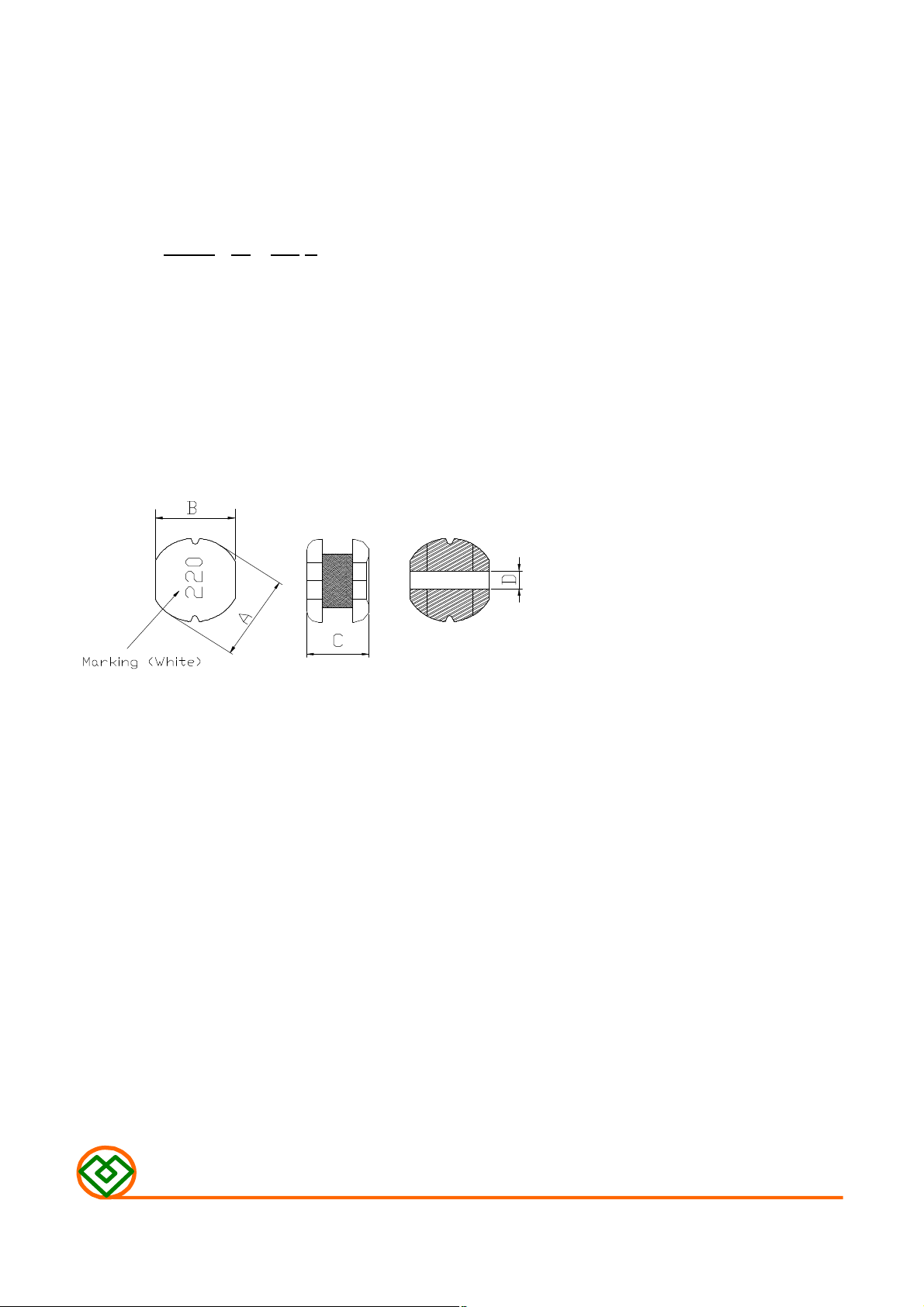
(1) SHAPES AND DIMENSIONS
(2) ELECTRICAL SPECIFICATIONS
(3) CHARACTERISTICS
MSCD-32-SERIES
PRODUCT INDENTIFICATION
MSCD - 32 - 100 K
① ② ③ ④
① Product Code
② Dimensions Code
③ Inductance Code
④ Tolerance Code
A: 3.3 ± 0.3 mm
B: 3.0 ± 0.3 mm
C: 2.1 ± 0.3 mm
D: 1.0 Typ. mm
SEE TABLE 1
TEST INSTRUMENTS
L : HP 4284A PRECISION LCR METER (or equivalent)
RDC : CHROMA MODEL 16502 MILLIOHMMETER (or equivalent)
(3)-1 Ambient temperature ……......... +60℃ Max.
(3)-2 Operate temperature range ...... -40℃~+125℃
(Including self temp. rise)
(3)-3 Storage temperature range ...... -40℃~+125℃
MAG.LAYERS
MSCD-32-SERIES Page 1/8
Page 2
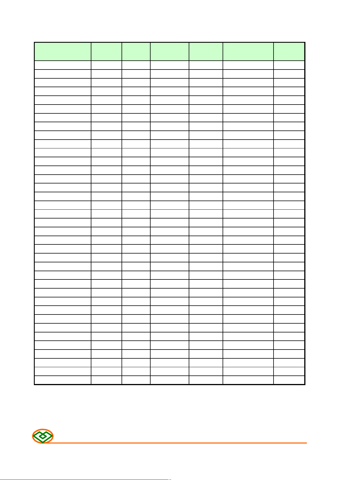
TABLE 1
MAGLAYERS
PT/NO.
MSCD-32-R47□
MSCD-32-1R0□
MSCD-32-1R4□
MSCD-32-1R5□ 1.86
MSCD-32-1R8□
MSCD-32-2R2□
MSCD-32-2R7□
MSCD-32-3R3□
MSCD-32-3R9□
MSCD-32-4R7□
MSCD-32-5R6□
MSCD-32-6R8□
MSCD-32-8R2□
MSCD-32-100□
MSCD-32-120□
MSCD-32-150□
MSCD-32-180□
MSCD-32-220□
MSCD-32-270□
MSCD-32-330□
MSCD-32-390□
MSCD-32-470□
MSCD-32-560□
MSCD-32-680□
MSCD-32-820□
MSCD-32-101□
MSCD-32-121□
MSCD-32-151□
MSCD-32-181□
MSCD-32-221□
MSCD-32-331□
MSCD-32-391□
MSCD-32-471□
MSCD-32-561□
MSCD-32-681□
MSCD-32-821□
MSCD-32-102□
Inductance Percent Test Resistance Rated DC Current
L(μH) Tolerance Frequency RDC(Ω)Max. IDC(A)
0.47 N 100kHz/0.25V 17.7m R47
1.0 M,N 100kHz/0.25V
1.4 M,N 100kHz/0.25V
1.5 M,N 100kHz/0.25V 90m 1R5
1.8 M,N 100kHz/0.25V
2.2 K,M,N 100kHz/0.25V
2.7 M,N 100kHz/0.25V
3.3 M,N 100kHz/0.25V
3.9 M,N 100kHz/0.25V
4.7 M,N 100kHz/0.25V
5.6 M,N 100kHz/0.25V
6.8 M,N 100kHz/0.25V
8.2 M,N 100kHz/0.25V
10 M 100kHz/0.25V
12 M 100kHz/0.25V
15 M 100kHz/0.25V
18 M 100kHz/0.25V
22 M 100kHz/0.25V
27 M 100kHz/0.25V 0.65 270
33 M 100kHz/0.25V 0.80 330
39 M 100kHz/0.25V
47 M 100kHz/0.25V
56 M 100kHz/0.25V
68 M 100kHz/0.25V
82 M 100kHz/0.25V
100 K,M 100kHz/0.25V
120 K,M 100kHz/0.25V
150 K,M 100kHz/0.25V
180 K,M 100kHz/0.25V
220 K,M 100kHz/0.25V
330 K,M 100kHz/0.25V
390 K,M 100kHz/0.25V
470 K,M 100kHz/0.25V
560 K,M 100kHz/0.25V
680 K,M 100kHz/0.25V
820 K,M 100kHz/0.25V
1000 K,M 100kHz/0.25V
70m
90m
0.11
0.13
0.14
0.17
0.19
0.21
0.22
0.25
0.28
0.32
0.35
0.40
0.48
0.58
0.90
1.19
1.27
1.73
1.99
2.52
2.90
3.36
4.03
5.64
9.24
10.14
11.48
19.49
22.00
23.98
28.80
3.00
2.08
1.86
1.80
1.39
1.32
1.25
1.20
1.03
0.91
0.85
0.82
0.74
0.64
0.60
0.54
0.50
0.43
0.37
0.36
0.33
0.30
0.29
0.25
0.20
0.19
0.17
0.17
0.14
0.12
0.09
0.08
0.08
0.07
0.06
0.05
Marking
1R0
1R4
1R8
2R2
2R7
3R3
3R9
4R7
5R6
6R8
8R2
100
120
150
180
220
390
470
560
680
820
101
121
151
181
221
331
391
471
561
681
821
102
※ □ specify the inductance tolerance,K(±10%),M(±20%),N(±30%)
※ IDC : Based on inductance change (△L/Lo:drop 10% Max.) @ ambient temperature 25℃ and
Based on temperature rise (△T: 40℃ TYP.)
MAG.LAYERS
MSCD-32-SERIES Page-2/8
Page 3
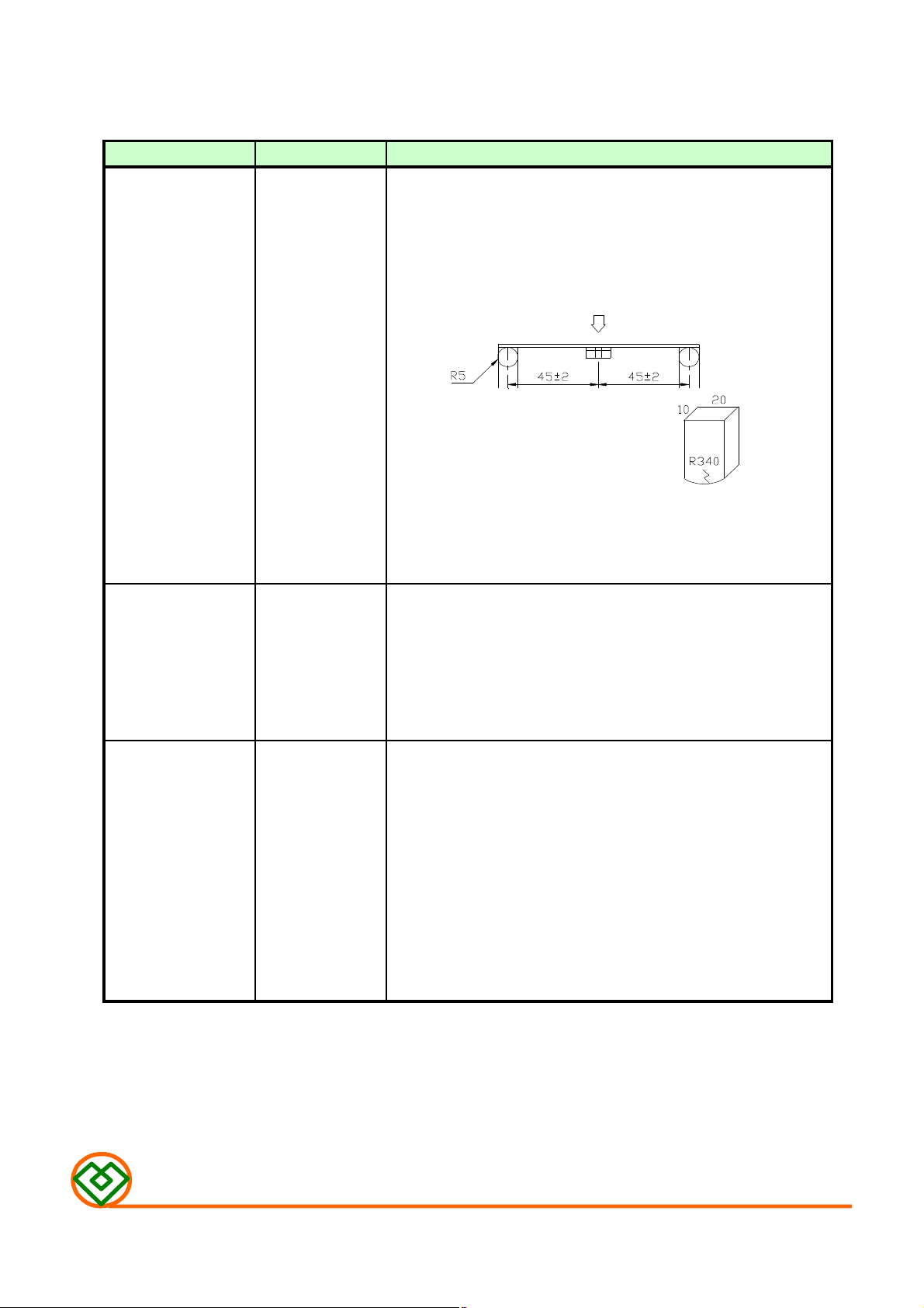
(4) RELIABILITY TEST METHOD
MECHANICAL
TEST ITEM SPECIFICATION TEST DETAILS
Substrate bending
△L/Lo≦±5%
There shall be direction is made approximately 3mm.(keep time 30 seconds)
no mechanical PCB dimension shall the page 7/9
damage or elec- F(Pressurization)
trical damege.
The sample shall be soldered onto the printed circuit board
in figure 1 and a load applied unitil the figure in the arrow
PRESSURE ROD
figure-1
Vibration
Solderability
△L/Lo≦±5%
There shall be and a frequency of from 10 to 55Hz/1 minute repeated should
no mechanical be applied to the 3 directions (X,Y,Z) for 2 hours each.
damage. (A total of 6 hours)
New solder Flux (rosin, isopropyl alcohol{JIS-K-1522}) shall be coated
More than 90% over the whole of the sample before hard, the sample shall
The sample shall be soldered onto the printed circuit board
and when a vibration having an amplitude of 1.52mm
then be preheated for about 2 minutes in a temperature of
130~150℃ and after it has been immersed to a depth 0.5mm
below for 3±0.2 seconds fully in molten solder M705 with
a temperature of 245±5℃.
More than 90% of the electrode sections shall be couered
with new solder smoothly when the sample is taken out of
the solder bath.
MAG.LAYERS
MSCD-32-SERIES
Page-3/8
Page 4

MECHANICAL
Sodering temperature (℃)
(230
℃)
TEST ITEM SPECIFICATION
Resistance to There shall be Temperature profile of reflow soldering
Soldering heat no damage or
(reflow soldering) problems.
300
250
soldering
(Peak temperature 260±3℃ 10 sec
200
150
100
50
Pre-heating
150 ~ 180℃
2 min
30 sec Min
+0
10
sec.
Slow cooling
(Stored at room
temperature)
2 min. or more
The specimen shall be passed through the reflow oven with the
condition shown in the above profile for 1 time.
The specimen shall be stored at standard atmospheric conditions
for 1 hour, after which the measurement shall be made.
ELECTRICAL
TEST ITEM SPECIFICATION TEST DETAILS
Insulation There shall be DC 100V voltage shall be applied across this sample of top
resistance no other surface and the terminal.
damage or
problems.
Dielectric There shall be AC 100V voltage shall be applied for 1 minute acrosset the top
withstand no other surface and the terminal of this sample
voltage damage or
problems.
Temperature
characteristics
△L/L20℃≦±10%
0~2000 ppm/℃ an ambient temperature of -20 to +85℃,and the value
The insulation resistance shall be more than 1 × 10⁸ Ω.
The test shall be performed after the sample has stabilized in
calculated based on the value applicable in a normal
temperature and narmal humidity shall be △L/L20℃≦±10%.
MAG.LAYERS
MSCD-32-SERIES
Page-4/8
Page 5

ENVIROMENT CHARACTERISTICS
TEST ITEM SPECIFICATION
High temperature
storage
△L/Lo≦±5%
There shall be Upon completion of the measurement shall be made after the
no mechanical sample has been left in a normal temperature and normal
damage. humidity for 1 hour.
The sample shall be left for 96±4 hours in an atmospere with
a temperature of 85±2℃ and a normal humidity.
Low temperature
storage
Change of
temperature subjected to standard atmospheric conditions for 1 hour,
Moisuture storage
Test conditions:
The sample shall be reflow soldered onto the printed circuit board in every test.
△L/Lo≦±5%
There shall be Upon completion of the test, the measurement shall be made
no mechanical after the sample has been left in a normal temperature and
damage. normal humidity for 1 hour.
△L/Lo≦±5%
There shall be after which measurement shall be made.
no other damage of problems
△L/Lo≦±5%
There shall be Upon completion of the test, the measurement shall be made
no mechanical after the sample has been left in a normal temperature and
damage. normal humidity more than 1 hour.
The sample shall be left for 96±4 hours in an atmosphere with
a temperature of -25±3℃.
The sample shall be subject to 5 continuos cycles, then it shall be
The sample shall be left for 96±4 hours in a temperature of
40±2℃ and a humidity(RH) of 90~95%.
MAG.LAYERS
MSCD-32-SERIES
Page-5/8
Page 6

(5) LAND DIMENSION (Ref.)
PCB: GLASS EPOXY t=1.6mm
(5)-1 LAND PATTERN DIMENSIONS
(STANDARD PATTERN) Unit : mm
3.5
Land
Part of silk screen
3.6
1.2
1.2
R1.0
(5)-2 SUBSTRATE BENDING TEST BENDING TEST BOARD
MAG.LAYERS
MSCD-32-SERIES Page-6/8
Page 7

(6) PACKAGING
(6)-1 CARRIER TAPE DIMENSIONS (mm)
12
(6)-2 TAPING DIMENSIONS (mm)
Unreeling
Direction
MAG.LAYERS
MSCD-32-SERIES
Page-7/8
Page 8

(6)-3 REEL DIMENSIONS (mm)
Tape width
(6)-4 QUANTITY
1000 pcs/Reel
The products are packaged so that no damage will be sustained.
:12
MAG.LAYERS
MSCD-32-SERIES
Page-8/8
 Loading...