M A COM MAAMSS0017TR3000, MAAMSS0017TR Datasheet

MAAMSS0017
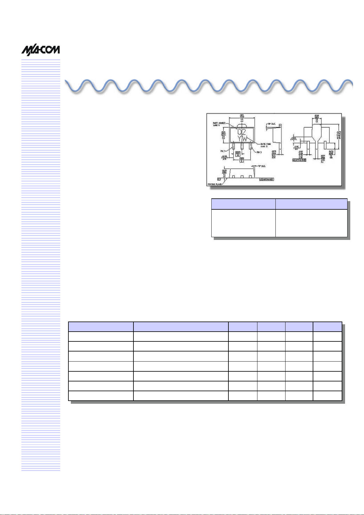
SOT-89 Plastic Package
V 1.00
Features
• Low Cost Plastic SOT-89 Package
• Broadband Operation
• Output Intercept Point of +40 dBm
• Output P1dB of +22 dBm
• High Efficiency
• 50 ohm Input /Output match
• Typical Gain of 18 dB
Description
M/A-COM’s MAAMSS0017 IF driver amplifier is a
GaAs MMIC which exhibits high OIP3 as well as high
gain and low power consumption in a low-cost miniature SOT89 surface mount plastic package. The
MAAMSS0017 employs a monolithic single stage
design featuring a convenient 50 ohm input/output
impedance that minimizes the number of external
components required. The device runs off a single
+5 volt supply and draws 70 mA typically. The design provides excellent performance from 50 to 450
MHz.
The MAAMSS0017 is fabricated using M/A-COM’s
iHBT process to realize low current and high power
functionality. The process features full passivation
for increased performance and reliability.
Parameter Test Conditions Units Min Typ Max
Gain2 F = 50-450 MHz dB 18
Noise Figure3 F = 50-450 MHz dB 4.4
Input Return Loss F = 50-450 MHz dB 12
Output Return Loss F = 50-450 MHz dB 15
1dB Compression F = 50-450 MHz dBm 22
Output IP3 4 F = 50-450 MHz dBm 40
Current Vs = 5 V mA 70
Electrical Specifications1: TA = +25° C, Vs = 5 V,Is = 70 mA
Broadband IF Driver Amplifier
50 - 450 MHz
Advanced
Part Number Package
MAAMMSS0017TR
MAAMSS0017TR3000
1000 Piece Tape and Reel
1
3000 Piece Tape and Reel
1
1. Reference Application Note M513 for reel size information.
1. All measurements taken in a 50 ohm system unless otherwise specified.
2. Gain varies at –0.008 dB/°C typical.
3. Noise figure varies at 0.007 dB/°C typical
4. OIP3 measured with Pout/Tone = +5 dBm, Tone spacing = 10 MHz

Broadband IF Driver Amplifier 50-450 MHz
MAAMSS0017
Specifications subject to change without notice.
n North America: Tel. (800) 366-2266
n Asia/Pacific: Tel.+81-44-844 -8296, Fax +81-44-844-8298
n Europe: Tel. +44 (1344) 869 595, Fax+44 (1344) 300 020
Visit www.macom.com for additional data sheets and product information.
V 1.00
2
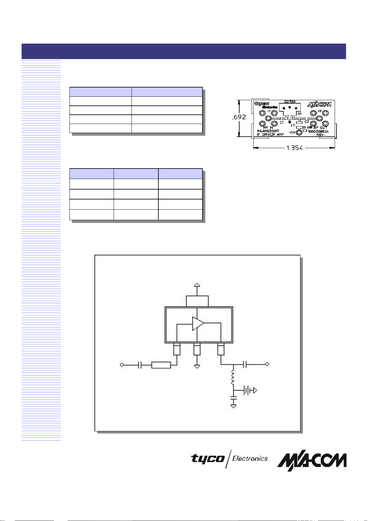
Schematic Including Off-Chip Components
Pin Configuration
Pin No. Function
1 RF In
2 GND
3 RF Out/Bias
4 GND
Off-Chip Component Values
Part Value Package
C1 100 pF 0603
C2 150 pF 0603
C3 10000 pF 0603
L1 180 nH 1008
Board Lay-out
RF In
Pin 1
100 mil
Z = 50 ohms
RF Out
C2
L1
C3
+ 5V
C1
 Loading...