M A COM MAAM71200-H1 Datasheet

Low Noise GaAs MMIC Amplifier
7.5 - 12 GHz
F e a t u r e s
●
2.7 dB Typical Noise Figure
●
15.5 dB Typical Gain
●
Single Bias Supply
●
Low Current Consumption
●
DC Decoupled RF Input and Output
●
Ceramic Package
D e s c r i p t i o n
M/A-COM’s MAAM71200-H1 is a wide band, low noise
GaAs MMIC amplifier enclosed in a leadless ceramic
p a c k a g e1. The MAAM71200-H1 is a packaged version of
M/A-COM’s MAAM71200 low noise MMIC amplifier chip.
The fully monolithic design operates in 50 ohms without
the need for external components.
The MAAM71200-H1 is ideally suited for micro s t r i p
assemblies where wire or ribbon bonds are used for interconnects. Typical applications include radar, EW and
communication systems.
MAAM71200-H1
V 2.00
C R - 1 6
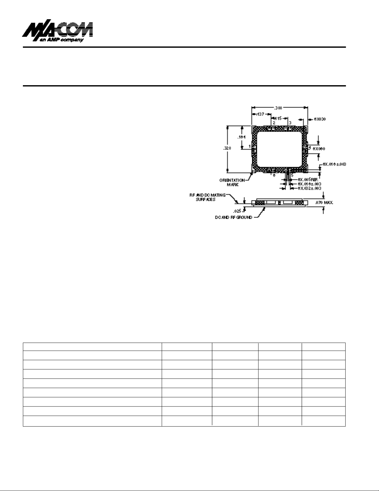
Dimensions are in inches.
The MAAM71200 is fabricated using a mature 0.5-micro n
gate length GaAs process for increased reliability and perf o rmance re p e a t a b i l i t y .
Typical Electrical Specifications,TA= +25°C,V
Parameter Units Min. Typ. Max.
Gain dB 14.5 15.5
Noise Figure dB 2.7 3.5
Input VSWR 2.0:1
Output VSWR 1.8:1
Output 1dB Compression Point dBm 11
Third Order Intercept Point dBm 21
Reverse Isolation dB 30
Bias Current (IDD) mA 40 55
1.Consult factory for a leaded ceramic package version.
D D
= 4 V

Low Noise GaAs MMIC Amplifier MAAM71200-H1
Pa r a m e t e r Absolute Maximu m
Input Powe r +20 dBm
V
D D
+9 Vo l t s
Junction Te m p e ra t u r e + 1 5 0 ° C
S t o rage Te m p e ra t u r e -65°C to +150°C
T h e rmal Resistance 1 7 5 ° C / W
Absolute Maximum Ratings
1
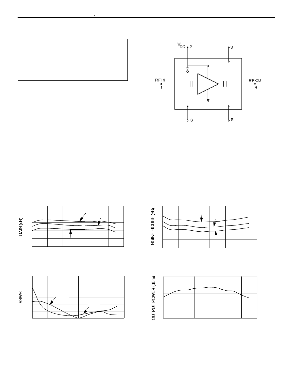
Typical Pe r formance
Functional Diag r am
1. Operation of this device outside any of these limits may
cause permanent damage
20
18
16
14
12
10
7 8 9 10 11 12 13
FREQUENCY (GHz)
4.0
3.5
3.0
2.5
2.0
1.5
1.0
7 8 9 10 11 12 13
FREQUENCY (GHz)
5
4
3
2
1
0
7 8 9 10 11 12 13
FREQUENCY (GHz)
GAIN vs FREQUENCY
INPUT & OUTPUT vs FREQUENCY
NOISE FIGURE vs FREQUENCY
+100°C
+100°C
-50°C
1. Case must be electrically connected to RF and DC ground.
2.The RF bond inductance from the transmission line to the
package is assumed to be 0.25 nH.Variations in bond
induc- tance will result in variations in VSWR and
gain slope. A small capacitive stub
may be needed depending on the
inductance realized in the final assembly.
3.Nominal bias is obtained by setting VDD= 4 volts.
4.Increasing VDDfrom 4 volts to 6 volts increases output
power and high frequency bandwidth.
+25°C
-50°C
+25°C
V 2.00
Output
Input
OUTPUT POWER @ 1dB COMPRESSION
vs FREQUENCY
15
13
11
9
7
5
7 8 9 10 11 12 13
FREQUENCY (GHz)
 Loading...