M A COM MAAM37000-A1G, MAAM37000-A1 Datasheet

L ow Noise GaAs MMIC Amplifier
3.5 - 7 GHz MAAM37000-A1
V 2.00
Features
●
Low Noise Figure: 2.2 dB
●
High Gain: 17 dB
●
Gain Flatness: ±0.5 dB
●
Single Supply: +4 V
●
No External Components Require d
●
DC Decoupled RF Input and Output
●
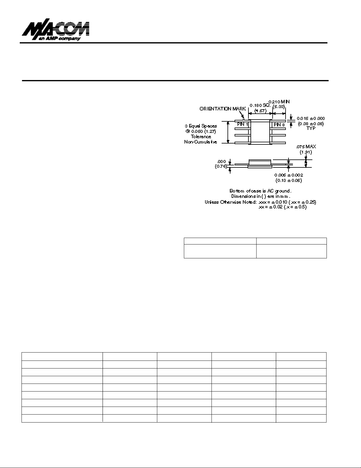
Small, 8-Lead Ceramic Package
D e s c r i p t i o n
M/A-COM’s MAAM37000-A1 is a wide band, low noise,
MMIC amplifier housed in a small 8-lead ceramic package. It includes two integrated gain stages and employs
series inductive feedback to obtain excellent noise figure
and a good, 50-ohm, input and output impedance match
over the entire frequency band. The MAAM37000-A1
operates from a single +4 V supply. It is fully monolithic,
re q u i res no external components, and is provided in a
u s e r-friendly, microwave package.
The MAAM37000-A1 perf o rms well as a low noise amplifier in receive applications and as a driver or buffer amplifier where high gain, excellent linearity and low power
consumption are important. Because of its wide bandwidth, the MAAM37000-A1 can be used in numero u s
c o m m e rcial and government system applications, such as
TVRO, VSAT, missile guidance and radar.
CR-3
Ordering Information
Part Number Package
MAAM37000-A1 8-Lead Ceramic
MAAM37000-A1G Gull Wing
The MAAM37000-A1 is manufactured in-house using a
reliable, 0.5-micron, GaAs MESFET process. This pro d u c t
is 100% RF tested to ensure compliance to perf o rm a n c e
s p e c i f i c a t i o n s .
Electrical Specifications
Test Conditions:TA= +25°C, Z0= 50 V,V
Parameter Units Min. Typ. Max.
Gain dB 15 17
Noise Figure dB 2.2 3.2
Input VSWR 2.0:1
Output VSWR 2.0:1
Output 1 dB Compression dBm +14
Input IP
Reverse Isolation dB 35
Bias Current mA 75 110
3
dBm +8
= +4 V, P
D D
= -30 dBm
I N

Low Noise GaAs MMIC Amplifier MAAM37000-A1
Parameter Absolute Maximum
V
DD
+7 volts
Input Power +20 dBm
Current 150 mA
Channel Temperature +150°C
Operating Temperature
2
-55°C to +100°C
Storage Temperature -65°C to +150°C
Absolute Maximum Ratings
1
Typical Performance @ +25°C
1. Operation of this device outside these limits may cause permanent
damage.
2. Typical thermal resistance ( jc) = +120°C/W
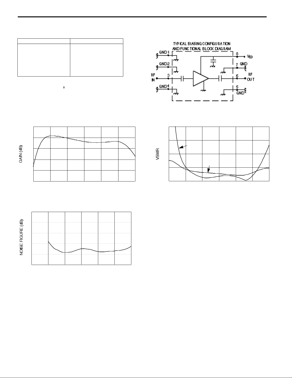
GAIN v s F R E QUENCY
2 3 4 5 6 7 8
20
18
16
14
12
10
FREQUENCY (GHz)
Schematic
V 2.00
NOISE FIGURE v s F R E QUENCY
6
VSWR v s F R E QU E N C Y
5.0
4.0
Input
3.0
Output
2.0
1.0
2 3 4 5 6 7 8
FREQUENCY (GHz)
5
4
3
2
1
2 3 4 5 6 7 8
FREQUENCY (GHz)
 Loading...