M A COM MAAM26100-P1 Datasheet

GaAs MMIC Power Amplifier
Preliminary Specifications
2 - 6 GHz
Features
●
+30 dBm Saturated Output Power
●
18 dB Typical Gain
●
30% Power Added Efficiency
●
On-Chip Bias Network
●
DC Decoupled RF Input and Output
●
High Performance Ceramic Bolt Down Package
Description
M/A-COM’s MAAM26100-P1 is a GaAs MMIC two stage
high efficiency power amplifier in a high performance
bolt down ceramic package. The MAAM26100-P1 is a
fully monolithic design for operation in 50-ohm systems,
with an on-chip negative bias network which eliminates
the need for external bias circuitry.
The MAAM26100-P1 is ideally suited for driver amplifiers
and transmitter outputs in Electronic Warfare Jammers,
Missile Subsystems and Phased Array Radars.
M/A-COM’s MAAM26100-P1 is fabricated using a mature
0.5-micron gate length GaAs process. The process
features full passivation for increased performance
reliability.
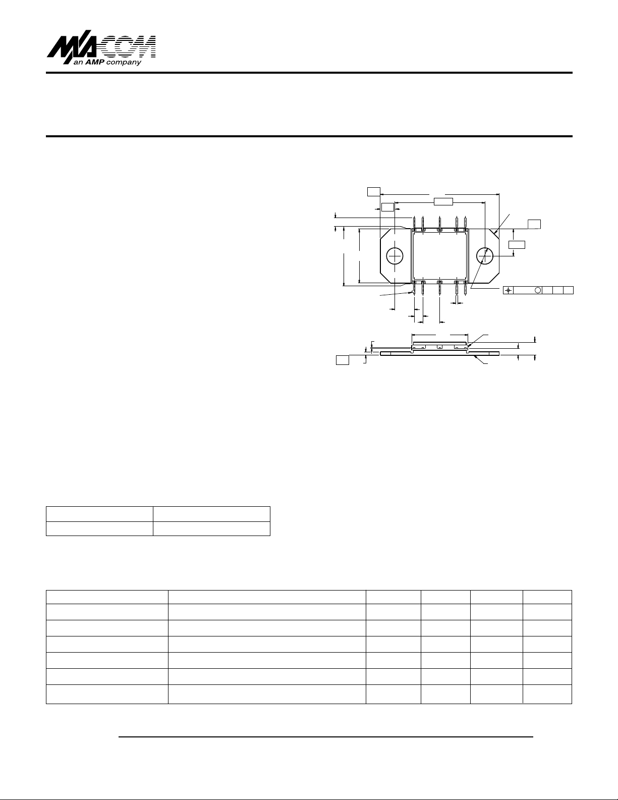
CR-15
-C-
10X .050 MIN
.328 ±.010
.318 ±.010
.010 SQ.
ORIENTATION TAB
.115
-A.020
MAAM26100-P1
.70
.085
10
±.010
.050
4X
.005±.002
Notes: (unless otherwise specified)
1. Dimensions are inches.
2. Tolerance: in .xxx = ±.010
.530
9
8
6
7
1
2
4
5
3
.010 ±.00310X
.1004X
.33
4X .06 X 45°
CHAMFER
.159
2X Ø
.096 THRU
Ø
.004 A BC
CERAMIC
.040
BASE PLATE
V1.A
-B-
M
.090MAX
Ordering Information
Part Number Package
MAAM26100-P1 Ceramic Bolt Down
Typical Electrical Specifications, T
Parameter Test Conditions Units Min. Typ. Max.
Small Signal Gain PIN≤ -10 dBm 2 - 6 GHz dB 18
Input VSWR PIN≤ -10 dBm 2 - 6 GHz 2.0:1
Output VSWR P
Output Power PIN= +15 dBm 2 - 6 GHz dBm +30
Power Added Efficiency PIN= +15 dBm 2 - 6 GHz % 30
Output IP
3
The Preliminary Specifications Data Sheet Contains Typical Electrical Specifications Which May Change Prior to Final Introduction.
M/A-COM, Inc.
North America: Tel. (800) 366-2266 ■ Asia/Pacific: Tel. +81 (03) 3226-1671 ■ Europe: Tel. +44 (1344) 869 595
Fax (800) 618-8883 Fax +81 (03) 3226-1451 Fax +44 (1344) 300 020
≤ -10 dBm 2 - 6 GHz 2.2:1
IN
= +25°C, VDD= +8 V, VGG= -5 V
A
2, 5 & 6 GHz dBm 40
1

GaAs MMIC Power Amplifier MAAM26100-P1
V1.A
Absolute Maximum Ratings
1, 2
Parameter Absolute Maximum
V
DD
V
GG
Power Dissipation 8.4 W
RF Input Power +23 dBm
Channel Temperature 150°C
Storage Temperature -65°C to +150°C
Thermal Resistance 15°C/W
(Channel to Case)
1. Exceeding these limits may cause permanent damage.
2. Case Temperature (Tc) = +25°C
10 Volts
-10 Volts
Typical Performance @+25°C
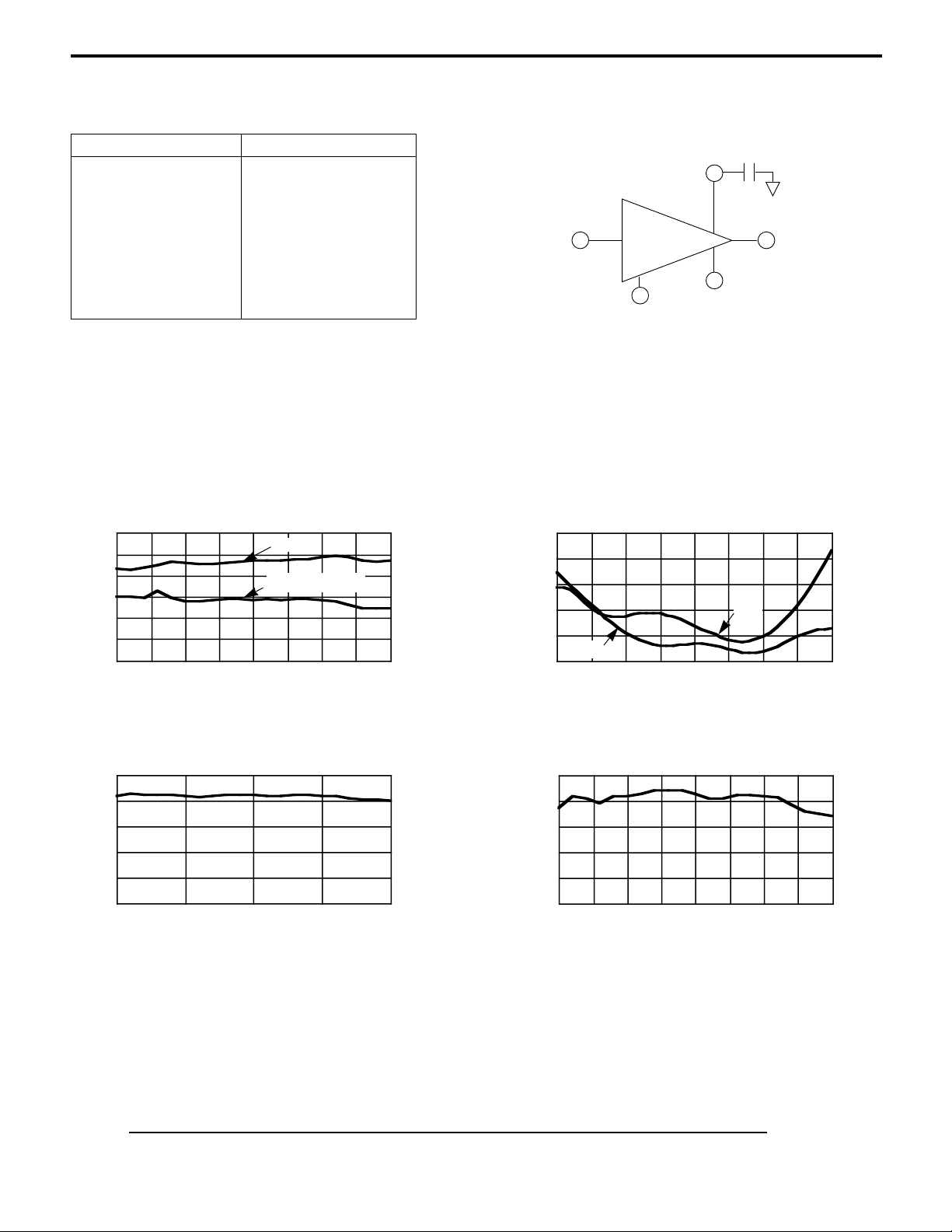
GAIN vs FREQUENCY
22
20
18
(dB)
16
21
S
14
12
10
2.0 2.5 3.0 3.5 4.0 4.5 5.0 5.5 6.0
FREQUENCY (GHz)
Linear
at PIN= +15dBm
Functional Diagram
3,4
0.01uF
V
DD
10
IN
3
MAAM26100-P1
OUT
8
6
V
GG
GND
1,2,4,5,7,9
3. Nominal bias is obtained by first connecting -5 volts to pin 6
(VGG),followed by connecting +9 volts to pin 10 (VDD).
Note sequence.
4. RF ground and thermal interface is the flange (case bottom).
Adequate heat sinking is required.
VSWR vs FREQUENCY
2.0
1.8
1.6
1.4
VSWR
1.2
1.0
S
11
2.0 2.5 3.0 3.5 4.0 4.5 5.0 5.5 6.0
FREQUENCY (GHz)
S
22
OUTPUT POWER vs FREQUENCY
= +15 dBm
@ P
IN
35
30
25
(dBm)
20
OUT
P
15
10
2.0 3.0 4.0 5.0 6.0
FREQUENCY (GHz)
The Preliminary Specifications Data Sheet Contains Typical Electrical Specifications Which May Change Prior to Final Introduction.
2
POWER ADDED EFFICIENCY vs FREQUENCY
@ PIN= +15 dBm
35
30
25
20
PAE (%)
15
10
2.0 2.5 3.0 3.5 4.0 4.5 5.0 5.5 6.0
FREQUENCY (GHz)
M/A-COM, Inc.
North America: Tel. (800) 366-2266 ■ Asia/Pacific: Tel. +81 (03) 3226-1671 ■ Europe: Tel. +44 (1344) 869 595
Fax (800) 618-8883 Fax +81 (03) 3226-1451 Fax +44 (1344) 300 020
 Loading...