M A COM MAALSS0012TR, MAALSS0012SMB, MAALSS0012-3000 Datasheet

Miniature Broadband Gain Sta ge
V 4.00
200 - 3000 MHz
Features
!
Low Noise Figure
!
High IP3
!
Single +3 V or +5 V Supply Voltage
!
Very Stable Over Temperature
Description
M/A-COM’s MAALSS0012 broadband gain stage is a
GaAs MMIC amplifier in a low-cost miniature SOT-363
surface mount plastic package. The MAALSS0012
employs a monolithic 1-stage self-biased design featuring a
convenient 50 ohm input/output impedance that minimizes
the number of external components required. The device
MAALSS0012
typically runs from a single 3.0 volt supply and may also
operate at any voltage up to 5.0 volts for improved powe r
performance. Its broadband design provides usable
performance from 200 to 3000 MHz.
M/A-COM fabricates the MAALSS0012 using an E/D
MESFET process to realize low noise and high dynamic
range. The process features full passivation for
performance and reliability.
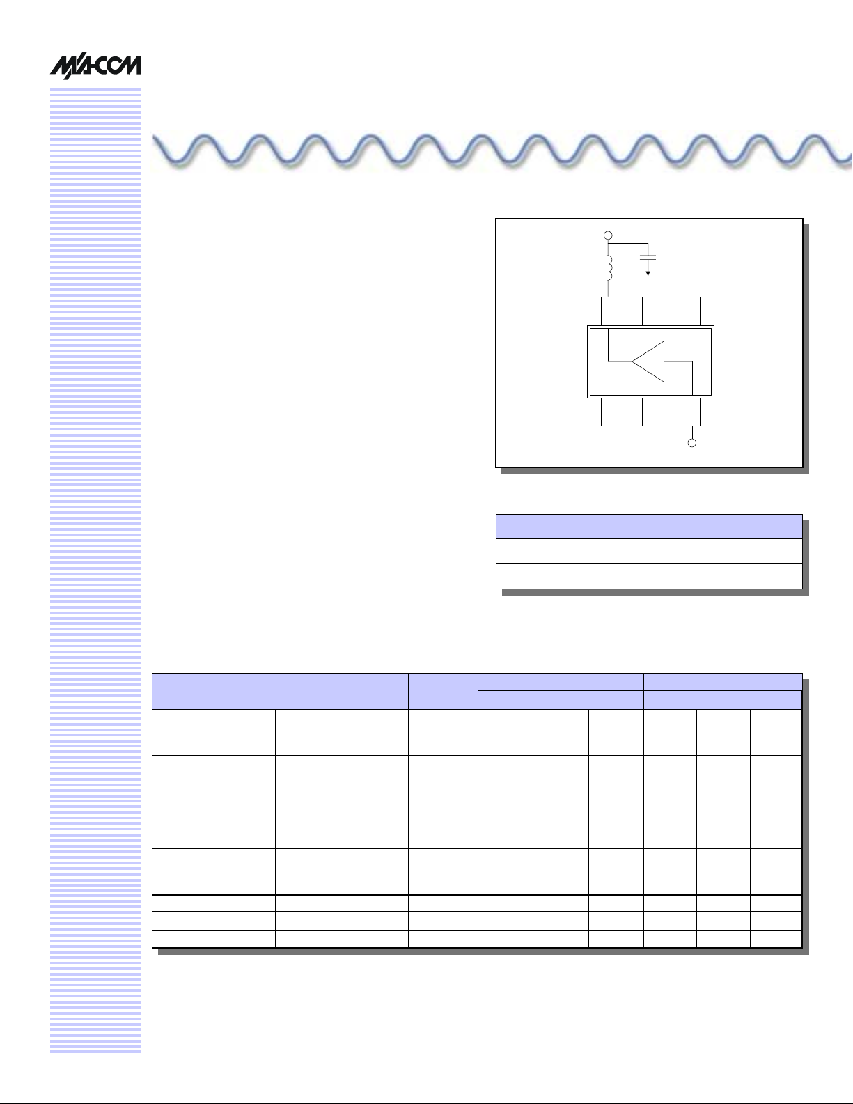
Functional Block Diagram
Vdd
Cdd
Ldd
RF OUT GND GND
PIN 6
PIN 1
GND GND RF IN
External Circuitry
Part Value Purpose
Cdd 470 pF Decoupling capacitor
Ldd 12 nH RF choke
Electrical Specifications1:
+3 V +5 V
Parameter Test Conditions Units
2
Gain
Noise Figure
Input Return Loss F = 0.9 GHz
Output Return Loss F = 0.9 GHz
1dB Compression 200 – 3000 MHz dBm 18 21
Output IP3 200 – 3000 MHz dBm 33 36
Current mA 50 79 95 65 87 100
1. All measurements taken in a 50-Ω system unless otherwise specified.
2. Gain varies at -0.0025 dB/°C typical.
3. Noise figure varies at 0.007 dB/°C typical.
3
F = 0.9 GHz
F = 1.9 GHz
F = 3.0 GHz
F = 0.9 GHz
F = 1.9 GHz
F = 3.0 GHz
F = 1.9 GHz
F = 3.0 GHz
F = 1.9 GHz
F = 3.0 GHz
TA = 25 °C
dB
dB
dB
dB
dB
dB
dB
dB
dB
dB
dB
dB
Min. Typ. Max. Min. Typ. Max.
13.0
10.9
1.4
9.3
9.0
14.0
11.9
9.4
1.4
1.5
13.2
14.9
15.2
27.0
15.0
12.9
2.0
2.0
9.4
9.7
13.2
11.0
1.5
14.2
12.0
9.6
1.5
1.6
13.2
14.7
15.5
33.0
15.2
13.0
2.0
2.0

Miniature Broadband Gain Stage, 200 - 3000 MHz
MAALSS0012
V 4.00
Absolute Maximum Ratings1
Parameter Absolute Maximum
RF Input Power 15 dBm
Voltage 6.0 volts
Operating Temperature
Storage Temperature -65 °C to +150 °C
1. Exceeding any one or combination of these limits may cause
permanent damage.
2. Minimum MTTF is 1x10
6
at +85°C, +5V, and 100 mA.
-40 °C to +85 °C
PIN Configuration
PIN Function Description
1 GND Ground
2 GND Ground
3 RF In RF input
4 GND Ground
5 GND Ground
1
6
1. Series inductor and decoupling capacitor recommended
on pin 6.
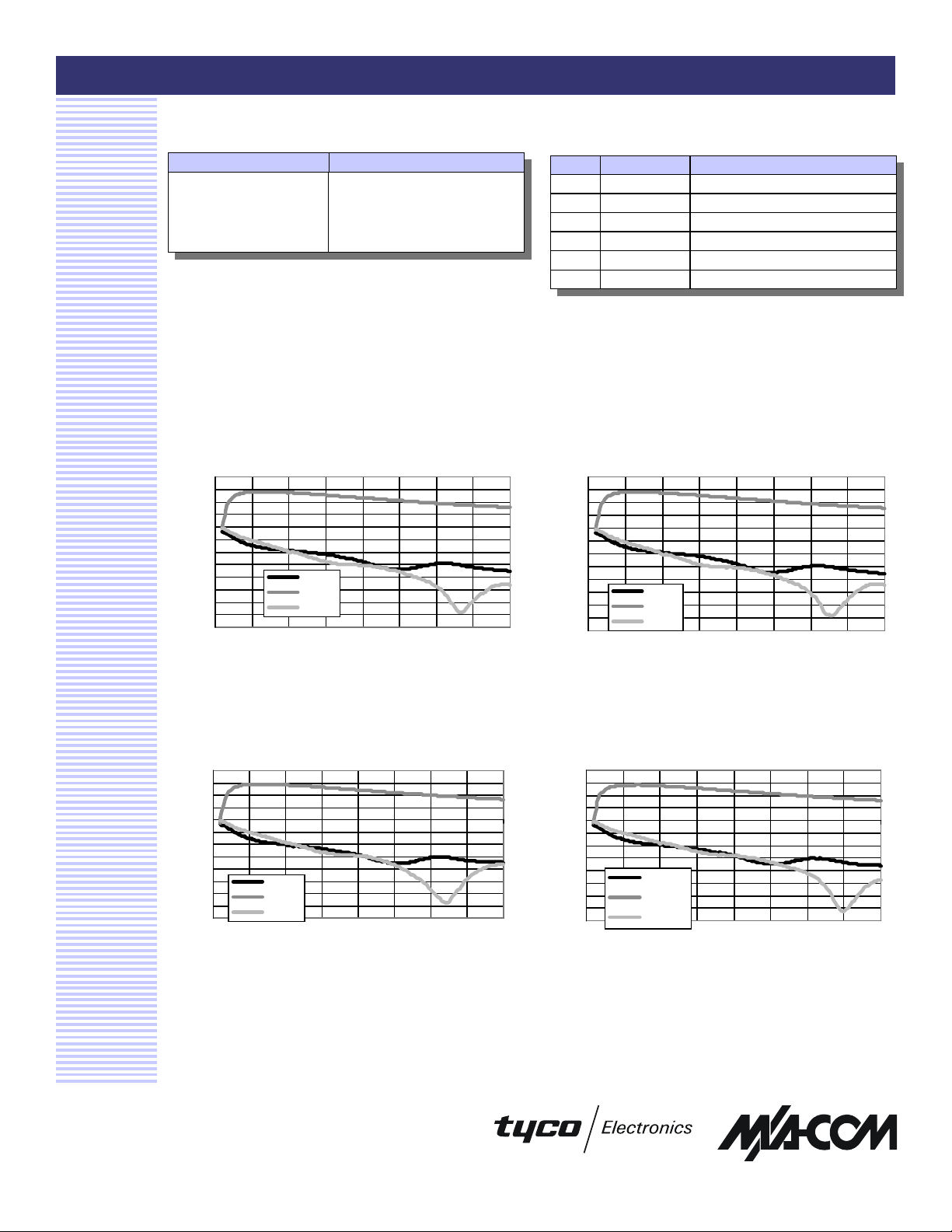
Typical Performance Curves
S-Parameters VDD @ 2.7 V, T = 25 °C
20
15
10
5
0
-5
-10
(dB)
-15
-20
-25
-30
-35
-40
0.0 0.5 1.0 1.5 2.0 2.5 3.0 3.5 4.0
S11 2.7V
S21 2.7V
S22 2.7V
FREQUE NCY ( G Hz )
S-Parameters VDD @ 3.0 V, T = 25 °C
20
15
10
5
0
-5
-10
(dB)
-15
-20
-25
-30
-35
-40
0.0 0.5 1.0 1.5 2.0 2.5 3.0 3.5 4.0
RF Out/VDD RF output & drain voltage input
S11 3.0V
S21 3.0V
S22 3.0V
FREQ UE NC Y ( G Hz)
S-Parameters VDD @ 5.0 V, T = 25 °C
20
15
10
5
0
-5
-10
(dB)
-15
-20
-25
-30
-35
-40
0.0 0.5 1.0 1.5 2.0 2.5 3.0 3.5 4.0
S11 5.0V
S21 5.0V
S22 5.0V
FREQUE NCY ( G H z)
Specifications subject to change without notice.
!
North America: Tel. (800) 366-2266
!
Asia/Pacif ic: Tel.+81-44-844-8296, Fax +81-44-844-8298
!
Europe: Tel. +44 (1344) 869 595, Fax+44 (1344) 300 020
Visit www.macom.com for additional data sheets and product information.
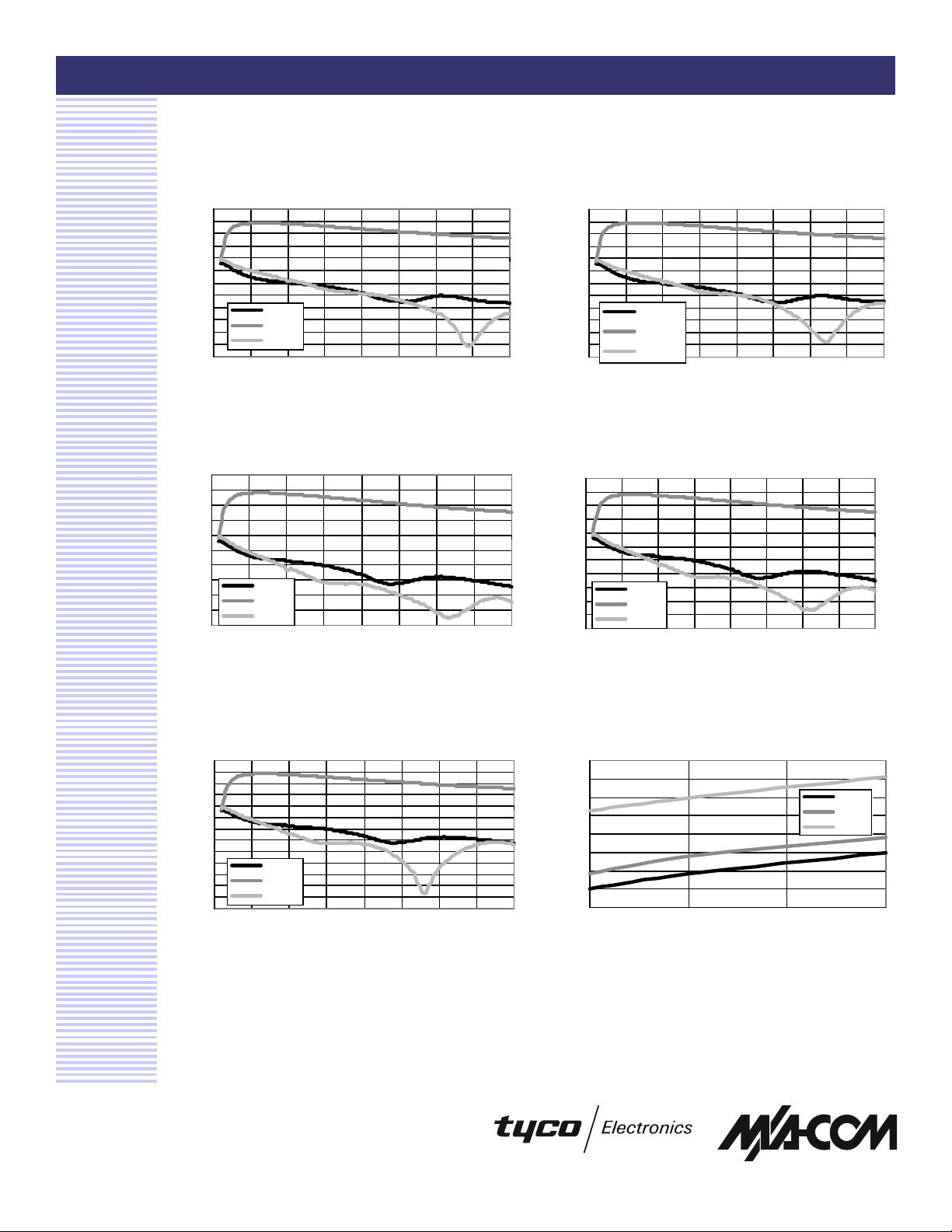
S-Parameters VDD @ 2.7 V, T = - 40° C
20
15
10
5
0
-5
-10
(dB)
-15
-20
-25
-30
-35
-40
0.0 0.5 1.0 1.5 2.0 2.5 3.0 3.5 4.0
S11 2.7V
S21 2.7V
S22 2.7V
FREQUE NCY ( G Hz )
2

Miniature Broadband Gain Stage, 200 - 3000 MHz
Typical Performance Curves (Cont’d)
MAALSS0012
V 4.00
S-Parameters VDD @ 3.0 V, T = - 40° C
20
15
10
5
0
-5
-10
(dB)
-15
-20
-25
-30
-35
-40
0.0 0.5 1.0 1.5 2.0 2.5 3.0 3.5 4.0
S-Parameters VDD @ 2.7 V, T = 70 °C
20
15
10
5
0
-5
(dB)
-10
-15
-20
-25
-30
0.0 0.5 1.0 1.5 2.0 2.5 3.0 3.5 4.0
S11 3.0V
S21 3.0V
S22 3.0V
FREQUE NCY ( G Hz)
S11 2.7V
S21 2.7V
S22 2.7V
FREQ UENCY (G Hz )
S-Parameters VDD @ 5.0 V, T = - 40 °C
20
15
10
5
0
-5
-10
(dB)
-15
-20
-25
-30
-35
-40
0.0 0.5 1.0 1.5 2.0 2.5 3.0 3.5 4.0
S-Parameters V
20
15
10
5
0
-5
-10
(dB)
-15
-20
-25
-30
-35
0.0 0.5 1.0 1.5 2.0 2.5 3.0 3.5 4.0
S11 5.0V
S21 5.0V
S22 5.0V
S11 3.0V
S21 3.0V
S22 3.0V
FREQUE NCY ( G Hz)
@ 3.0 V, T = 70 °C
DD
FREQUE NCY ( G Hz)
S-Parameters VDD @ 5.0 V, T = 70 °C
20
15
10
5
0
-5
-10
-15
(dB)
-20
-25
-30
-35
-40
-45
0.00.51.01.52.02.53.03.54.0
S11 5.0V
S21 5.0V
S22 5.0V
FREQ UE NC Y ( G Hz)
Specifications subject to change without notice.
!
North America: Tel. (800) 366-2266
!
Asia/Pacif ic: Tel.+81-44-844-8296, Fax +81-44-844-8298
!
Europe: Tel. +44 (1344) 869 595, Fax+44 (1344) 300 020
Visit www.macom.com for additional data sheets and product information.
Output IP
38
37
36
35
34
(dBm)
3
33
IP
32
31
30
0.5 1.0 1.5 2.0
at 25 °C
3
FREQUE NCY ( G Hz )
IP3 2.7V
IP3 3.0V
IP3 5.0V
3
 Loading...