

Quad PIN Diode π Attenuator
5 –3000 MHz
MA4P274-1225T
Features
n 4 PIN Diodes in SOT-25 Plastic Package
n Externally Selectable Bias and RF Match Network
n 5 – 3,000 MHz Useable Frequency Band
n + 43 dBm IP3@ 1 GHz (50 Ω)
n 1.0 dB Loss @ 1 GHz (50 Ω)
n 30 dB Attenuation @ 1 GHz (50 Ω)
Description
M/A-COM's MA4P274-1225 is a wideband, lower insertion
loss, high IP3, Quad PIN Diode π Attenuator in a low-cost,
surface mount SOT-25 package. Four PIN Diodes in one
package reduce design parasitics and improve circuit
density.
Applications
These PIN Diode Attenuators perform well where RF
Signal Amplitude Control is required in 50 Ω Handset
Circuits and 75 Ω Broadband CATV Systems. Exceptional
Insertion Loss, Attenuation Range, and IP3 at <10 mA bias
make these devices suitable for better power level control in
RF Amplifiers.
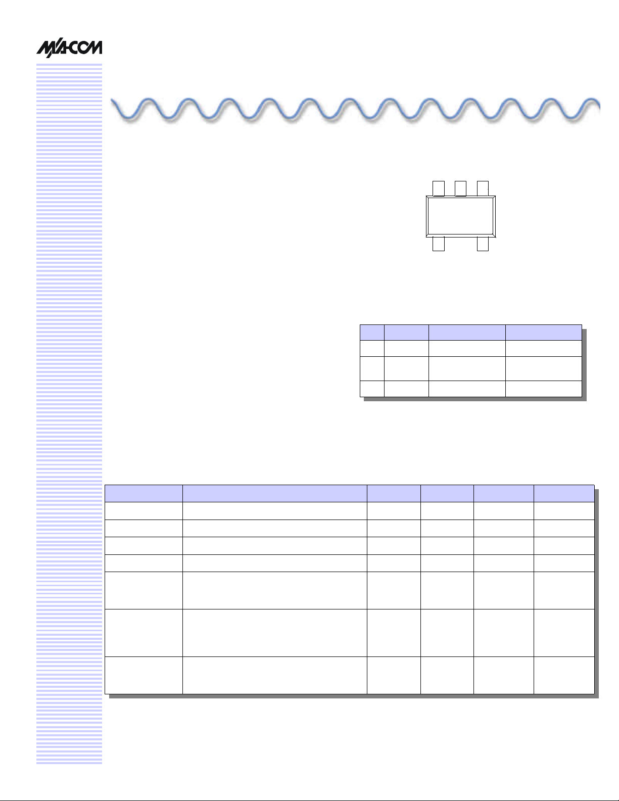
Package Outline (Topview)
3 2 1
Topview
4
5
PIN Configuration
PIN Function PIN Function
1 RF In 4 Shunt 1 Bias
2 Series
Bias
3 RF Out
5 Shunt 2 Bias
Guaranteed Electrical Specifications: @ +25 °C
Parameter Test Conditions Units Min. Typ. Max.
Ct @ 0 V 100 MHz pF 0.45 0.50
Rs @ 1 mA 100 MHz
Rs @ 10 mA 100 MHz
Vb D.C. V 125 150
Minority Carrier
Lifetime
Power
Dissipation
RF Incident
Power
( 50 % - 90 % ) Voltage
If = + 10mA, Ir = - 6mA Pulse
@ 100 kHz Sq Wave
D.C. and F = 5 – 3,000 MHz
Derate linearly to 0 mW at 125 C
Using 1,000 deg-C/W
Thermal Resistance
F = 5 – 3,000 MHz
Vshunt 1 & 2 Diode Bias = 0.75 V
Vseries Diode Bias = 0 to 20 V
Ω
Ω
nS 1000 2000
mW 100
dBm + 20
13 18
2.3 3.0
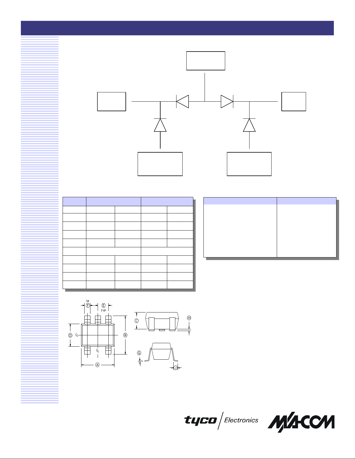
Quad PIN Diode π Attenuator
PIN 1:
RF In
Series Bias
RF Out
Functional Schematic
MA4P274-1225, V 3.00
MA4P274-1225T
PIN 3:
PIN 4 :
Shunt 1 Bias
Case Style: SOT 25
Dim Inches
Min. Max. Min. Max.
A .1103 .1181 2.80 3.10
B .1023 .1181 2.6 3.00
C 0.0355 .0512 0.9 1.30
D 0.0591 .0669 1.5 1.70
E .0374 REF.
F .0138 .0197 .35 .50
G .0031 0.0079 .08 0.2
H .0002 .0059 .05 .15
J .0138 .0216 .35 .55
Millimeters
0.95 REF.
PIN 2:
PIN 5 :
Shunt 2 Bias
Absolute Maximum Ratings1
Parameter Absolute Maximum
Operating Temperature
Storage Temperature,
No Dissipated Power
DC Voltage at Temperature
Extremes
DC Current at 25 °C
Mounting Temperature
1. Exceeding any one or combination of these limits may cause
permanent damage.
-65 °C to +125 °C
-65 °C to +150 °C
-100 V
75 mA
+235 °C for 10 seconds
Specifications subject to change without notice.
n North America: Tel. (800) 366-2266
n Asia/Pacific: Tel.+81-44-844-8296, Fax +81-44-844-8298
n Europe: Tel. +44 (1344) 869 595, Fax+44 (1344) 300 020
Visit www.macom.com for additional data sheets and product information.
1. Dimensions do not include mold peaks, protrusion or
gate burrs which shall not exceed 0.0098 in.
(.25) mm per side.
2. Leads Coplanarity should be 0.003 (0.08) mm Max.
2
Quad PIN Diode π Attenuator
Typical 50 Ω SOT-25 RF Performance @ +25 °C using Wideand RF Circuit Design
( Values Shown include Through Loss Calibrated Out of RF Test Circuit )
Parameter Frequency Range Test Conditions Units Min. Typ. Max.
Insertion Loss 5 – 1,000 MHz
Insertion Loss 5 – 1,000 MHz
Return Loss 5 – 1,000 MHz
Attenuation 5 – 1,000 MHz
Input IP3 5 – 1,000 MHz
Input IP3 5 – 1,000 MHz
Input IP3 5 – 1,000 MHz
Input IP3 5 – 1,000 MHz
Settling Time 5 – 1,000 MHz Within 1 dB of Final Attenuation Value
RF C.W. Incident
Power
5 – 1,000 MHz 0 – 20 V Series Diode Bias
+ 3 mA / Series Diode
and 0.75 V Shunt 1 and 2 Bias
F = 1 GHz
+ 6.5 mA / Series Diode
and 0.75 V Shunt 1 and 2 Bias
F = 1 GHz
+ 6.5 mA / Series Diode
and 0.75 V Shunt 1 and 2 Bias
F = 1 GHz
0 mA / Series Diode
and 0.75 V Shunt 1 and 2 Bias
F = 1 GHz
0 mA / Series Diode
and 0.75 V Shunt 1 and 2 Bias
F1 = 1000 MHz, F2 = 1100 MHz
+ 6.5 mA / Series Diode
and 0.75 V Shunt 1 and 2 Bias
F1 = 1000 MHz, F2 = 1100 MHz
0 mA / Series Diode
and 0.75 V Shunt 1 and 2 Bias
F1 = 100 MHz, F2 = 110 MHz
+ 6.5 mA / Series Diode
and 0.75 V Shunt 1 and 2 Bias
F1 = 100 MHz, F2 = 110 MHz
F = 1 GHz
and 0.75 V Shunt 1 and 2 Bias
MA4P274-1225, V 3.00
dB -2.0
dB -1.0
dB -10
dB -29
dBm 43
dBm 43
dBm 43
dBm 33
uS 3
dBm + 20
MA4P274-1225T
Typical 75 Ω SOT-25 RF Performance @ +25 °C using Wideand RF Circuit Design
( Values Shown include Through Loss Calibrated Out of RF Test Circuit )
Parameter Frequency Range Test Conditions Units Min. Typ. Max.
Insertion Loss 5 – 1,000 MHz
Insertion Loss 5 – 1,000 MHz
Attenuation 5 – 1,000 MHz
Return Loss 5 – 1,000 MHz
Specifications subject to change without notice.
n North America: Tel. (800) 366-2266
n Asia/Pacific: Tel.+81-44-844-8296, Fax +81-44-844-8298
n Europe: Tel. +44 (1344) 869 595, Fax+44 (1344) 300 020
Visit www.macom.com for additional data sheets and product information.
+ 2 mA / Series Diode
and 1.0 V Shunt 1 and 2 Bias
+ 4.5 mA / Series Diode
and 1.0 V Shunt 1 and 2 Bias
0 mA / Series Diode
and 1 V Shunt 1 and 2 Bias
+ 4.5 mA / Series Diode
and 1.0 V Shunt 1 and 2 Bias
dB -1.1
F = 1 GHz
dB -0.6
F = 1 GHz
dB -27
F = 1 GHz
dB -10
F = 1 GHz
3

Quad PIN Diode π Attenuator
Frequency @ 0 V
1.00
1000
MA4P274-1225, V 3.00
MA4P274-1225T
MA4P274-1225 Diode Rs vs I MA4P274-1225 Diode Ct vs
100 MHz
0.10
1.00 10.00 100.00 1000.00 10000.00
F ( MHz )
MA4P274-1225 Attenuation vs Frequency in
50 Ohms, Shunt Bias = 0.75 V
-5
-15
-25
Series Diode: 10 V
Series Diode: 0 V
-35
-45
-55
-65
50 150 250 350 450 550 650 750 850 950
Frequency ( MHz )
Series Diode: 5 V
Series Diode: 1 V
RS vs. IF @ 100 MHz and 1 GHz
100
10
1
0.01 0.10 1.00 10.00 100.00
4 MHz
900 MHz
I ( mA )
MA4P274-1225 Return Loss vs Frequency in
50 Ohms, Shunt Bias = 0.75 V
0
-5
-10
Series Diode: 1 V
-15
Series Diode: 0 V
-20
-25
50 150 250 350 450 550 650 750 850 950
Series Diode: 2 V
Series Diode: 3 V
Series Diode: 5
Series Diode: 10 V
Frequency ( MHz )
LS vs. Frequency @ 10 mA
Specifications subject to change without notice.
n North America: Tel. (800) 366-2266
n Asia/Pacific: Tel.+81-44-844-8296, Fax +81-44-844-8298
n Europe: Tel. +44 (1344) 869 595, Fax+44 (1344) 300 020
Visit www.macom.com for additional data sheets and product information.
4

Quad PIN Diode π Attenuator
MA4P274-1225 IP3 vs Series Voltage,
Vshunt = .075 V
60
55
50
45
40
35
30
25
20
0 2 4 6 8 10 12 14 16 18 20
F1 = 1000 MHz, F2 = 1100 MHz
F1 = 100 MHz, F2 = 110 MHz
Series Diode Voltage ( V )
MA4P274-1225, V 3.00
MA4P274-1225T
MA4P274-1225 Insertion Loss vs Frequency in 75
Ohms, Shunt Bias = 1 V
-1.4
-1.2
Series Current per Diode = 2 mA
-1
-0.8
Series Current per Diode = 4.5 mA
-0.6
-0.4
-0.2
0
20.00 142.50 265.00 387.50 510.00 632.50 755.00 877.50 1000.00
Frequency (MHz)
MA4P274-1225 Attenuation vs Frequency in
75 Ohms, Shunt Bias = 1 V
-70
-60
-50
-40
-30
-20
-10
0
20.00 142.50 265.00 387.50 510.00 632.50 755.00 877.50 1000.00
Series Diode: 0.5 V
Series Diode: 0.7 V
Series Diode: 1 V
Series Diode: 2 V
Series Diode: 3 V
Series Diode: 20 V
Frequency (MHz)
Specifications subject to change without notice.
n North America: Tel. (800) 366-2266
n Asia/Pacific: Tel.+81-44-844-8296, Fax +81-44-844-8298
n Europe: Tel. +44 (1344) 869 595, Fax+44 (1344) 300 020
Visit www.macom.com for additional data sheets and product information.
5

Quad PIN Diode π Attenuator
PIN 1:
RF In
RF Out
Series Bias
5 - 1,000 MHz Wideband RF Circuit
10K pF 10K pF
PIN 3:
1 K ohms
MA4P274-1225, V 3.00
MA4P274-1225T
10K pF
PIN 2:
1 K ohms
10K pF
1 K ohms
X2
PIN 4 :
Shunt 1 Bias
Note : Keeping PIN 4 & PIN 5 as Separate Bias Points ( Same V ) reduces RF leakage ( increases attenuation ) through an
otherwise connected Common Anode Bias Node.
PIN 5 :
Shunt 2 Bias
10 - 1,000 MHz Wideband RF Circuit Parts List
Item Supplier Supplier P/N
4003 or 4350 Circuit Board
4003 ( εr = 3.38), 4350 ( εr = 3.48 )
Capacitor, 10 K pF
3.2 mm L x 1.6 mm W x 1.15 mm H
Resistor, 1K Ω
1.0 mm L x 0.5 mm w x 0. 25 mm H
Rogers Corporation
www.rogers-corp.com
Murata
www.murata.com
Piconics
www.piconics.com
RO4003 , RO4350
GRM42-6COH103K25PB
C1001BC42KSA
Specifications subject to change without notice.
n North America: Tel. (800) 366-2266
n Asia/Pacific: Tel.+81-44-844-8296, Fax +81-44-844-8298
n Europe: Tel. +44 (1344) 869 595, Fax+44 (1344) 300 020
Visit www.macom.com for additional data sheets and product information.
6

Quad PIN Diode π Attenuator
Series and Shunt Diode Bias Currents as a Function of Vseries and
Vshunt Voltage Using Wideband RF Circuit
(Values shown are PER DIODE )
MA4P274-1225, V 3.00
MA4P274-1225T
Vshunt Bias ( V ) Vseries Bias ( V ) Iseries Diode ( mA )
0.75 0 0.000
0.75 1 0.106
0.75 2 0.443
0.75 3 0.773 0
0.75 4 1.099 0
0.75 5 1.426 0
0.75 6 1.750 0
0.75 7 2.092 0
0.75 8 2.424 0
0.75 9 2.756 0
0.75 10 3.088 0
Ishunt Diode ( mA )
0.192
0.120
0.048
0.75 11 3.421 0
0.75 12 3.754 0
0.75 13 4.087 0
0.75 14 4.410 0
0.75 15 4.743 0
0.75 16 5.081 0
0.75 17 5.406 0
0.75 18 5.750 0
0.75 19 6.079 0
0.75 20 6.413 0
Specifications subject to change without notice.
n North America: Tel. (800) 366-2266
n Asia/Pacific: Tel.+81-44-844-8296, Fax +81-44-844-8298
n Europe: Tel. +44 (1344) 869 595, Fax+44 (1344) 300 020
Visit www.macom.com for additional data sheets and product information.
7
Quad PIN Diode π Attenuator
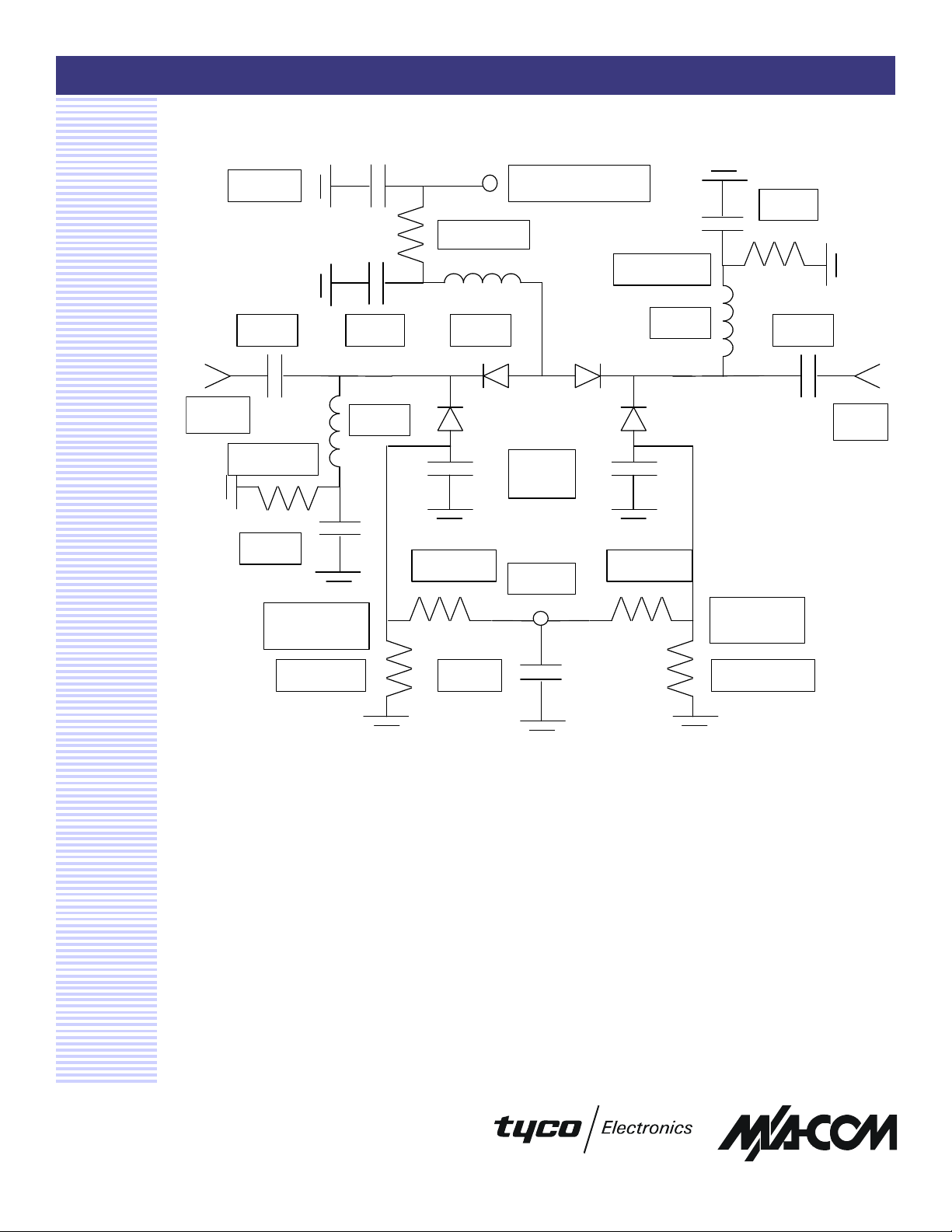
PIN 1:
RF In
RF Out
Vc = 0
–
5 V
1 – 3 GHz 50 Ω, Higher Frequency, Lower Tuning Voltage RF Circuit
MA4P274-1225, V 3.00
MA4P274-1225T
PIN 3:
0.1 uF
56 pF
330 ohms
56 pF
PIN 4 :
Shunt 1 Bias
56 pF
22 nH
PIN 2: Series Bias
100 ohms
330 ohms
22 nH
22 nH
680 pF
( 2 X )
1 K ohms 1 K ohms
+ 5 V
56 pF
56pF
PIN 5 :
Shunt 2 Bias
0.1 uF
Note : Keeping PIN 4 & PIN 5 as Separate Bias Points ( Same V ) reduces RF leakage through an otherwise connected
Common Anode Bias Node.
Specifications subject to change without notice.
n North America: Tel. (800) 366-2266
n Asia/Pacific: Tel.+81-44-844-8296, Fax +81-44-844-8298
n Europe: Tel. +44 (1344) 869 595, Fax+44 (1344) 300 020
Visit www.macom.com for additional data sheets and product information.
180 ohms 180 ohms
8

Quad PIN Diode π Attenuator
1 - 3 GHz Higher Frequency RF Circuit Parts List
Item Supplier Supplier P/N
MA4P274-1225, V 3.00
MA4P274-1225T
4003 or 4350 Circuit Board
4003 ( εr = 3.38), 4350 ( εr = 3.48 )
Capacitor, .01 uF, Power Supply Filter
1.6 mm L x 0.80 mm W x .080 mm H
Capacitor, 680 pF, Diode RF Bypass
2.0 mm L x 1.5 mm W x .085 mm H
Capacitor, 56 pF, D.C. Block,
RF Decoupling
1.0 mm L x 0.5 mm W x 0.5 mm H
Inductor, 22 nH, RF Choke
Resistor, 100 Ω
1.0 mm L x 0.5 mm w x 0. 25 mm H
Resistor, 180 Ω
1.0 mm L x 0.5 mm w x 0. 25 mm H
Resistor, 330 Ω
1.0 mm L x 0.5 mm w x 0. 25 mm H
Resistor, 1K Ω
1.0 mm L x 0.5 mm w x 0. 25 mm H
Rogers Corporation
www.rogers-corp.com
Murata
www.murata.com
Murata GRM40COG681K50PB
Murata GRM36COG560K50PB
Coilcraft
www.coilcraft.com
Piconics
www.piconics.com
Piconics C1800BC42KSA
Piconics C3300BC42KSA
Piconics
RO4003 , RO4350
GRM39X7R104K25PB
1812SMS-22NJ
C1001BC42KSA
C1001BC42KSA
Specifications subject to change without notice.
n North America: Tel. (800) 366-2266
n Asia/Pacific: Tel.+81-44-844-8296, Fax +81-44-844-8298
n Europe: Tel. +44 (1344) 869 595, Fax+44 (1344) 300 020
Visit www.macom.com for additional data sheets and product information.
9
Quad PIN Diode π Attenuator
P2
P1
C
C C9
L L3
L L2
L L1
L L4
R R1
C C5
C C4
C C8
R R4
C C3
R R2
C C2
C C1
R R3
C C6
C C7
wBV
Af=1
2
Tau=1.0
usec
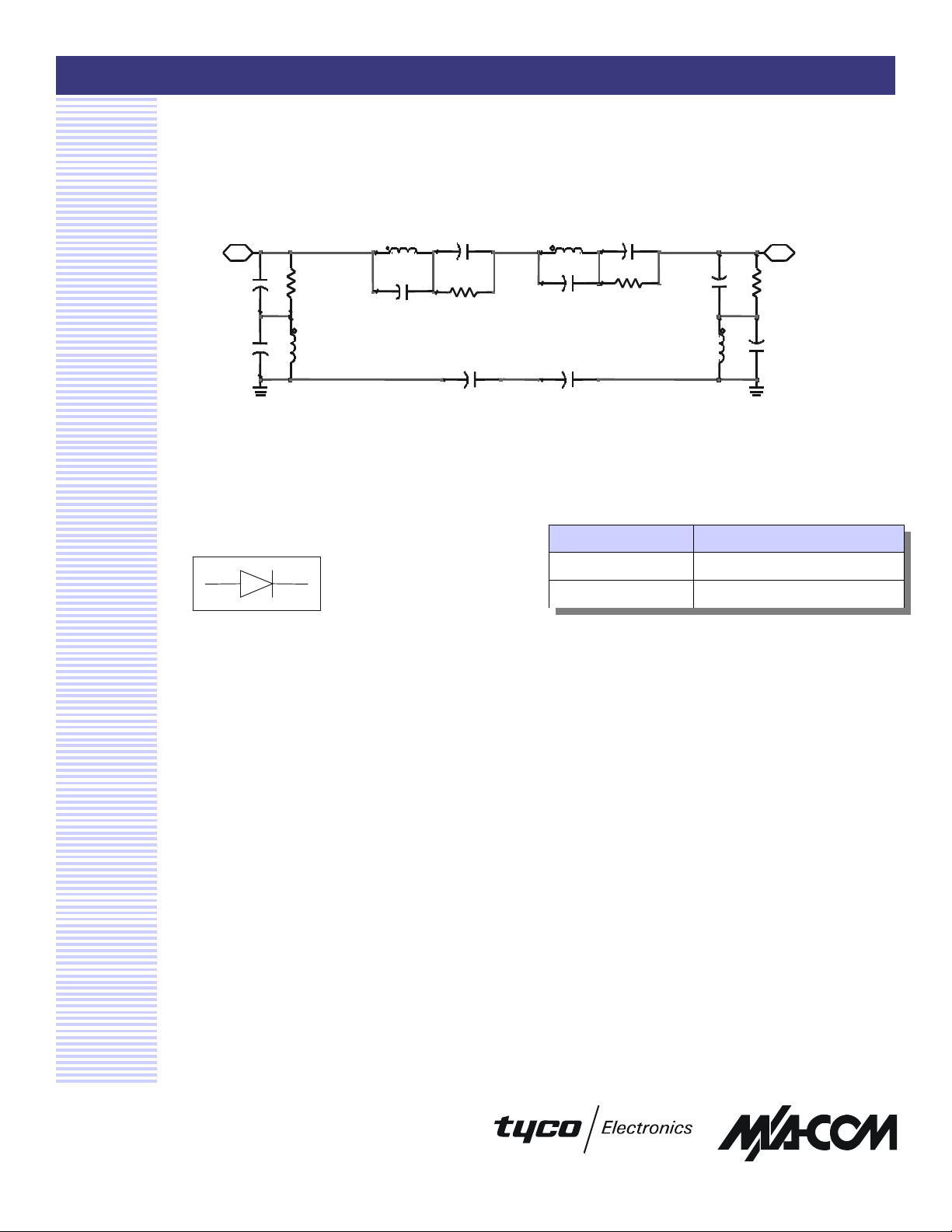
Lumped Model of SOT-25, MA4P274-1225 PIN Diode π Quad Attenuator
Port
Num=1
L=0.8 nH
C=0.27pF
L=0.8 nH
C=0.27 pF
MA4P274-1225, V 3.00
MA4P274-1225T
Port
Num=2
C=0.27 pF
C=0.05 pF
R=Rjsh Ohm
L=0.8 nH
C=0.05pF
R=Rjse Ohm
C=0.0003 pF
MA4P274-1225 SPICE MODEL
Pin Diode Model
NLPINM2
Is=1E-14 A
Vi=0 V
Un=900 cm2/V-sec
Wi=60 um
Rr=1.25 Ohm
Cmin=0.20 pF
C=0.27 pF
C=0.05pF
C10
C=0.0003 pF
R=Rjse Ohm
L=0.8 nH
Ordering Information
Model Number Package
MA4P274 -1225 Tube
MA4P274 -1225T Tape and Reel
R=Rjsh Ohm
C=0.05 pF
Rs=0.1 Ohm
Cjo=0.27 pF
Vj=0.7 V
M=0.5
Fc=0.5
Imax=2.5E+6 A/m
Kf=0
Ffe=1
= 150 V
Specifications subject to change without notice.
n North America: Tel. (800) 366-2266
n Asia/Pacific: Tel.+81-44-844-8296, Fax +81-44-844-8298
n Europe: Tel. +44 (1344) 869 595, Fax+44 (1344) 300 020
Visit www.macom.com for additional data sheets and product information.
10
 Loading...