

Page 1

1
IBAYT-PBL3
(motherboard card)
AD1040
(daughter card)
Intel® Bay Trail SOC
Atom™ J1900
Startup Manual
V1.0
Page 2

2
Copyright
The documentation and the software included with this product are copyrighted 2015 by
LONGSHINE Technology GmbH. All rights are reserved. LONGSHINE Technology GmbH reserves
the right to make improvements in the products described in this manual at any time without notice.
No part of this manual may be reproduced, copied, translated or transmitted in any form or by any
means without the prior written permission of LONGSHINE Technology GmbH. Information
provided in this manual is intended to be accurate and reliable. However, LONGSHINE Technology
GmbH assumes no responsibility for its use, nor for any infringements of the rights of third parties,
which may result from its use.
Safety Declaration
The manufacturer reserves the right to make changes, without notice, to any product, including
circuits and/or software described or contained in this manual in order to improve design and/or
performance. The manufacturer assumes no responsibility or liability for the use of the described
product(s), conveys no license or title under any patent, copyright, or masks work rights to these
products, and makes no representations or warranties that these products are free from patent,
copyright, or mask work right infringement, unless otherwise specified. For the detail product
information, please refer to user’s manual.
Safety Instructions
1. Read these safety instructions carefully.
2. Keep this User Manual for later reference.
3. Disconnect this equipment from any AC outlet before cleaning. Use a damp cloth. Do not use
liquid or spray detergents for cleaning.
4. For plug-in equipment, the power outlet socket must be located near the equipment and must be
easily accessible.
5. Keep this equipment away from humidity.
6. Put this equipment on a reliable surface during installation. Dropping it or letting it fall may cause
damage.
7. The openings on the enclosure are for air convection. Protect the equipment from overheating.
DO NOT COVER THE OPENINGS.
8. Make sure the voltage of the power source is correct before connecting the equipment to the
power outlet.
9. Position the power cord so that people cannot step on it. Do not place anything over the power
cord.
10. All cautions and warnings on the equipment should be noted.
11. If the equipment is not used for a long time, disconnect it from the power source to avoid
damage by transient overvoltage.
12. Never pour any liquid into an opening. This may cause fire or electrical shock.
13. Never open the equipment. For safety reasons, the equipment should be opened only by
qualified service personnel.
Page 3

3
14. If one of the following situations arises, get the equipment checked by service personnel:
The power cord or plug is damaged.
Liquid has penetrated into the equipment.
The equipment has been exposed to moisture.
The equipment does not work well, or you cannot get it to work according to the user's
manual.
The equipment has been dropped and damaged.
The equipment has obvious signs of breakage.
15. DO NOT LEAVE THIS EQUIPMENT IN AN ENVIRONMENT WHERE THE STORAGE
TEMPERATURE MAY GO BELOW -20° C (-4° F) OR ABOVE 60° C (140° F). THIS COULD
DAMAGE THE EQUIPMENT. THE EQUIPMENT SHOULD BE IN A CONTROLLED
ENVIRONMENT.
16. CAUTION: DANGER OF EXPLOSION IF BATTERY IS INCORRECTLY REPLACED.
REPLACE ONLY WITH THE SAME OR EQUIVALENT TYPE RECOMMENDED BY THE
MANUFACTURER, DISCARD USED BATTERIES ACCORDING TO THE MANUFACTURER'S
INSTRUCTIONS.
The sound pressure level at the operator's position according to IEC 704-1:1982 is no more than 70
dB (A).
DISCLAIMER: This set of instructions is given according to IEC 704-1. LONGSHINE Technology
GmbH disclaims all responsibility for the accuracy of any statements contained herein.
Safety Precaution - Static Electricity
Follow these simple precautions to protect yourself from harm and the products from damage.
To avoid electrical shock, always disconnect the power from your PC chassis before you work on it.
Don't touch any components on the CPU card or other cards while the PC is on.
Disconnect power before making any configuration changes. The sudden rush of power as you
connect
Page 4

1. General Introduction
1.1 Product Overview
IBAYT-PBL3 is designed with Intel® Celeron™ J1900 SoC for industrial applications that request
performance computing and reliable stability. The motherboard has on board CPU Intel® Celeron™
J1900 Quad core 2.0 GHz.
IBAYT-PBL3 has rich I/O connectivity with PS/2, COM port, LAN, USB port and audio Jack
integrated in a customerized form factor. It also supports dual display for LVDS and VGA.
IBAYT-PBL3 also comes with plenty of connectivity and expansion options. 8-bit GPIO, mini PCIe
expansion slot and PCIe x 1 slot enable easy integration. 10/100/1000 Mbps Ethernet port is also
available to deliver high speed networking.
1.2 Specifications
Specifications
System
CPU
BayTrail-D Intel® Celeron® Processor J1900
2GHz/2M Cache (Quad core)
BIOS AMI 64Mb SPI ROM
Memory
- 2GB memory as Standard, Max. 8GB
-
DDR3L-133 SO-DIMM Socket x 2 (Horizental type); 4GB on each
SO-DIMM)
Watchdog Timer
256-level Watchdog Timer
H/W Status Monitor
Monitoring System Temperature and Voltages
Expansion Slots
1 x Full-size mini-PCIe Socket (for Wireless LAN)
1 x mSATA Solid State Drive (SSD) slot (optional)
Wake up / Boot on LAN LAN (WOL,PXE)
Smart Fan Control Yes
Display
Chipset Intel® Integrated Graphics Engine (Dual Display Support)
Internal Display
2 x LVDS (Single Channel 24bits + Dual Channel 24bits) With Chrontel CH7511B IC
Internal Display
1 x DB-15 VGA ; Max resolution: 2048 x 1536
Touch IC
5-wired Flat Resistive Touch (EETI touch controller defined in daughter board)
Audio
Audio Codec Realtek® ALC892 HD Audio
Audio Amp 6W Audio Amp
Ethernet
LAN1 Intel® i211-AT PCIe Gigabit Ethernet Controller
Page 5

External IO Ports
Serial Port
External:
- 4 x RS-232 Ports (RJ45 type)
- COM1/2/3/4
- 0V/+5V/+12V power output by BIOS adustable; default 0V
USB Port
4 x USB 2.0
Cash Drawer Port
- 1 x RJ-11
- +12/+24V power output by BIOS adjustable; default +24V
Keyboard/ Mouse
1 x PS2 (Keyboard/Mouse Auto Detection)
LAN Port
1 x RJ-45 GigLAN
VGA
1 x VGA (DB15)
4 pin DIN type
1x DIN (4P) 19V
Internal Connectors
Memory Slot
2 x SO-DIMM memory slot (Horizontal)
LVDS
1 x LVDS1 (30-pin Single Channel 24-bit)
1 x LVDS2 (40-pin, Dual Channel 24-bit)
LVDS Power
1 x LVDS PWR select (2x3 pin header for 3.3V/5V select)
SATA
SATA1: 1 x SATA 22p
SATA2: 1 x mSATA
Clear CMOS Jumper
1 x CMOS Clear (1x3 pin header)
BIOS Flash
1 x SPI for BIOS flash (2x4 pin header)
Speaker out
1 x speaker out (1x2 pin header with R & L channel)
mini PCIe
- 1 x mini PCIe
- with USB signal
Serial Port
Internal :
- 2 x RS-232 PIN Header
- 0/12V/5V power output by BIOS adjustable; default 0V
For Touch controller:
- 1 x RS-232 PIN Header
- 0/12V/5V power output by BIOS adjustable; default +5V
USB Port
2 x USB 2.0 PIN Header(2x6 wafer)
1 x USB 2.0 PIN Header(1x4 wafer)
1 x USB 2.0 (in mini-PCIe)
Printer Port
1 x LPT (2x13 box header)
Battery
1 x Button Cell with wire (Horizontal paste on selected area)
Buzzer
1 x Buzzer
CPU/system fan
connector
Optional CPU/System fan (1x4 for CPU and 1x3 for SYS pin header)
Page 6

6
1.3 Platform Features and Benefits
Integrated Gfx (Intel® HD Graphics) supports embedded hardware decode accelerator deliver
1080p HD video stream with excellent performance.
DirectX® 11.1 & Open GL 4.0 let you enjoy awesome graphics performance, stunning 3D visual
effect and dynamic interactivity
Memory support low voltage DDR3 memory controller
Operating system support:
– Windows 7 32 bit / 64 bit
– Windows 8 32 bit / 64 bit
– Fedora 18 Remix / Yocto
Page 7

7
2. Product Introduction / Installation
2.1 Before you Proceed
Take note of the following precautions before you install motherboard components or change any
motherboard settings.
Caution!
Unplug the power cord from the wall socket before touching any component.
Use a grounded wrist strap or touch a safely grounded object or a metal object, such as
the power supply case, before handling components to avoid damaging them due to static
electricity
Hold components by the edges to avoid touching the ICs on them.
Whenever you uninstall any component, place it on a grounded anti-static pad or in the
bag that came with the component.
Before you install or remove any component, ensure that the ATX power supply is
switched off or the power cord is detached from the power supply. Failure to do so may
cause severe damage to the motherboard, peripherals, and/or components.
2.2 Motherboard Overview
Before you install the motherboard, study the configuration of your chassis to ensure that the
motherboard fits into it. Refer to the chassis documentation before installing the motherboard.
Warning!
Make sure to unplug the power cord before installing or removing the motherboard. Failure to do so
can cause you physical injury and damage motherboard components.
2.2.1 Placement Direction
When installing the motherboard, make sure that you place it into the chassis in the correct
orientation. The edge with external ports goes to the rear part of the chassis as indicated in the
image below.
2.2.2 Screw Holes
Place screws into the holes indicated by circles to secure the motherboard to the chassis.
Caution!
Do not over tighten the screws! Doing so can damage the motherboard.
Page 8
8
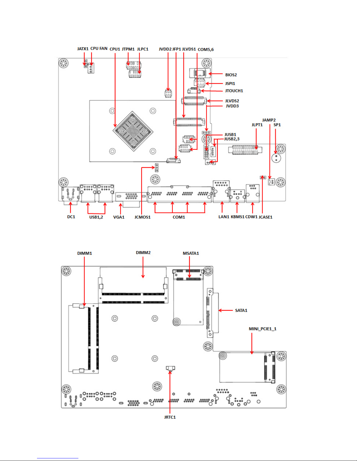
2.2.3 Motherboard Layout
IBAYT-PBL3 Top side:
IBAYT-PBL3 Bottom side:
Page 9
9
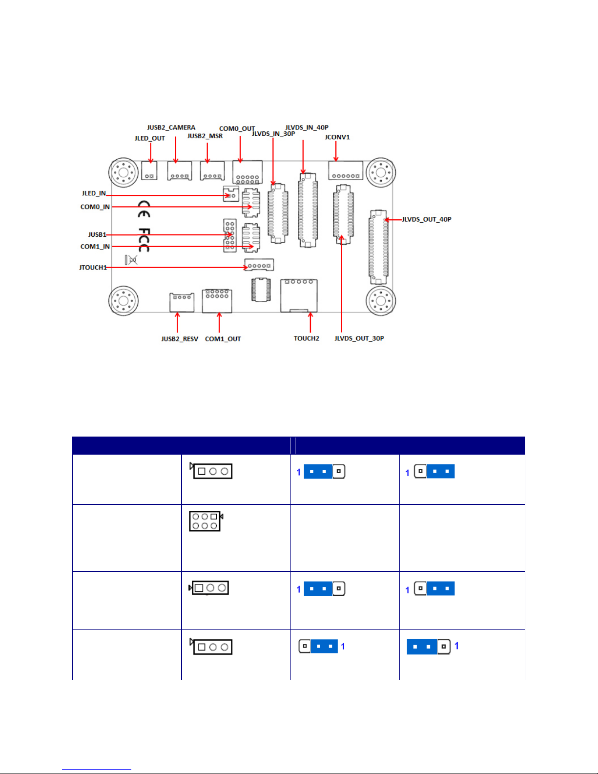
2.2.4 Daughterboard Layout
AD1040 TOP side:
2.2.5 Jumper Content and Function List
Jumpers:
Label Function Note
JATX1
ATX/AT SELECTION
AT mode
ATX mode(default)
JVDD2
JLVDS2 Power select
1-3 (default): 3.3V
3-5: 5V
For LVDS2_VDD
2-4 (default): 3.3V
4-6: 5V
For JBKLVOL2
JVDD3
JLVDS2 Converter
Power select
5V
12V
JCMOS1
Clear CMOS
NA
Clear CMOS
Page 10
10
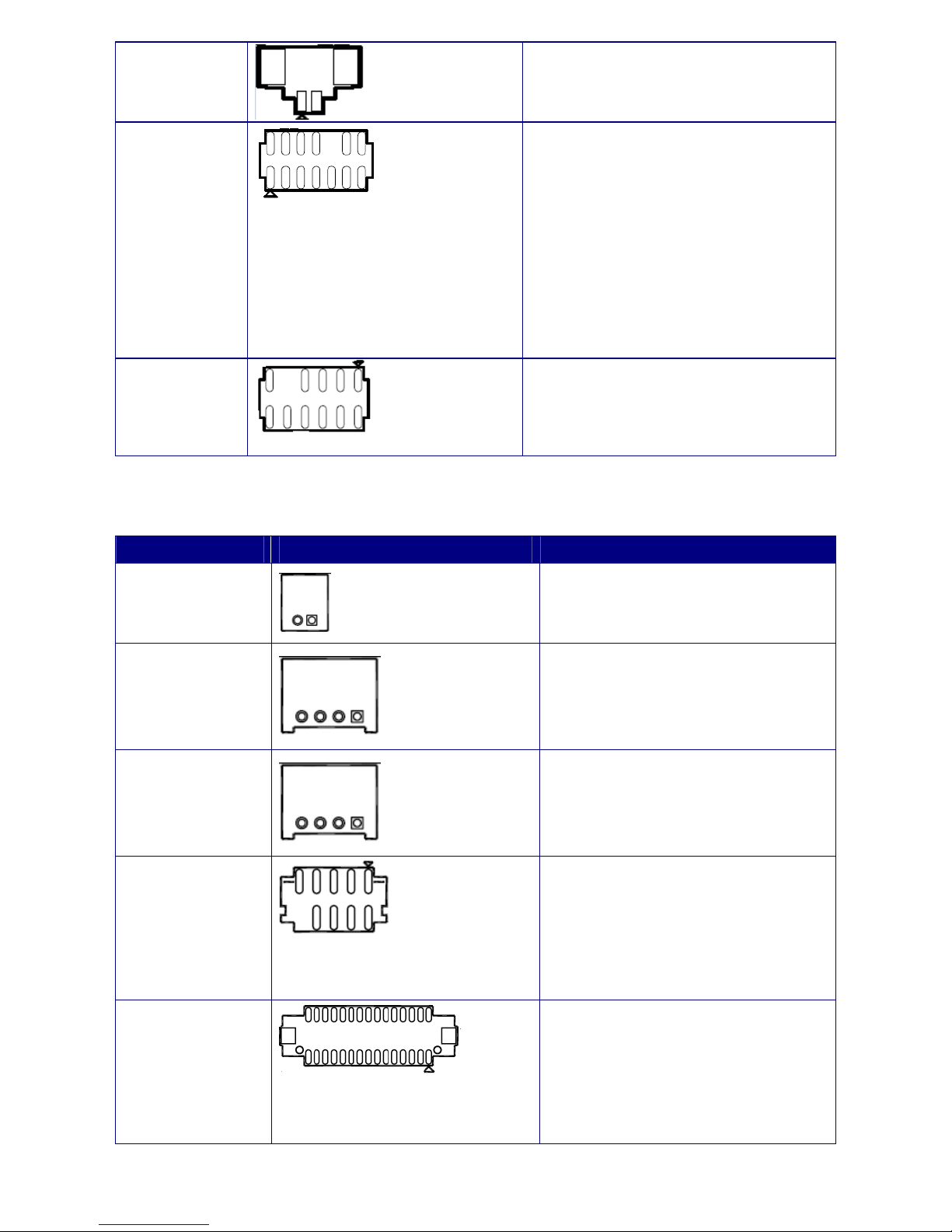
2.2.6 MB Internal Connector and PIN Definition
Label Function Note
CPU_FAN
1.GND
2.12V
3.CPUFAN_DEC
4.CPUFAN_PWM
JFP1
PIN1 : +5VSB
PIN2 : PWR_LED#
PIN3 : PANSWIN#
PIN4 : GND
PIN5 : PMC_RST_BTN#_D
PIN6 : GND
JLVDS1
LVDS Connector
PIN1 : +12V_BL PIN21: LVDSA_N3
PIN2 : +12V_BL PIN22: LVDSA_N2
PIN3 : LVDS1_VDD L PIN23: GND
PIN4 : +12V_BL PIN24: GND
PIN5 : LVDS1_VDD PIN25: LVDSB_P1
PIN6 : LVDS1_VDD PIN26: LVDSB_P0
PIN7 : LVDS1_EDID_CLK PIN27: LVDSB_N1
PIN8 : LVDS1_EDID_DATA PIN28: LVDSB_N0
PIN9 : BRIGHT1 PIN29: GND
PIN10 : LVDS_VDD_EN PIN30: GND
PIN11 : BL_EN PIN31: LVDSB_P3
PIN12 : LVDS1_DETECT#_C PIN32: LVDSB_P2
PIN13 : LVDSA_P1 PIN33: LVDSB_N3
PIN14 : LVDSA_P0 PIN34: LVDSB_N2
PIN15 : LVDSA_N1 PIN35: GND
PIN16 : LVDSA_N0 PIN36: GND
PIN17 : GND PIN37: LVDSB_CLK_P
PIN18 : GND PIN38: LVDSA_CLK_P
PIN19 : LVDSA_P3 PIN39: LVDSB_CLK_N
PIN20 : LVDSA_P2 PIN40: LVDSA_CLK_N
COM5,6
Serial Port Connector
PIN1 : COM1_DCD#
PIN2 : COM1_RXD
PIN3 : COM1_TXD
PIN4 : COM1_DTR#
PIN5 : GND
PIN6 : COM1_DSR#
PIN7 : COM1_RTS#
PIN8 : COM1_CTS#
PIN9 : C1_RID#
JSPI1
SPI debug port
PIN1 : +1.8V_SPI
PIN2 : GND
PIN3 : SPISKT_CS0#
PIN4 : SPISKT_CLK
PIN5 : SPISKT_MISO
PIN6 : SPISKT_MOSI
PIN7 : SPISKT_HOLD0#
Page 11
11
JTOUCH1
PIN1: +5V
PIN2: +3.3V
PIN3: TOUCH_232_RXD
PIN4: TOUCH_232_TXD
PIN5: GND
JLVDS2
LVDS Connector
PIN1 : Conv_SRC PIN16 : LVDS2A_N2
PIN2 : LVDS2A_P3 PIN17 : LVDS2_VDD
PIN3 : Conv_SRC PIN18 : GND
PIN4 : LVDS2A_N3 PIN19 : LVDS2_VDD
PIN5 : BL_EN2 PIN20 : LVDS2A_P1
PIN6 : GND PIN21: +3.3V
PIN7 : BRIGHT2 PIN22: LVDS2A_N1
PIN8 : LVDS2A_CLK_P PIN23: GND
PIN9 : NC PIN24: GND
PIN10 : LVDS2A_CLK_N PIN25: LVDS2_EDID_DATA
PIN11 : LVDS2_DETECT#_C PIN26: LVDS2A_P0
PIN12 : GND PIN27: LVDS2_EDID_CLK
PIN13 : GND PIN28: LVDS2A_N0
PIN14 : LVDS2A_P2 PIN29: GND
PIN15 : GND PIN30: GND
JUSB1
PIN1: USB_HB_CM_P4 PIN7: USB_HB_CM_P2
PIN2: +5V_USB789 PIN8: USB_HB_CM_P3
PIN3: USB_HB_CM_N4 PIN9 : USB_HB_CM_N2
PIN4: +5V_USB789 PIN10: USB_HB_CM_N3
PIN5: GND PIN11: +5V_USB789
PIN6: GND PIN12: +5V_USB789
JUSB2,3
PIN1: +5V_USB56
PIN2: USB_CM_N2
PIN3: USB_CM_P2
PIN4: GND
JLPT1
PIN1 : LPT_STB# PIN14: GND
PIN2 : LPT_AFD# PIN15: LPT_PD6
PIN3 : LPT_PD0 PIN16: 16.GND
PIN4 : LPT_ERR# PIN17: LPT_PD7
PIN5 : LPT_PD1 PIN18: GND
PIN6 : LPT_INIT# PIN19: LPT_ACK#
PIN7 : LPT_PD2 PIN20: GND
PIN8 : LPT_SLIN# PIN21: LPT_BUSY
PIN9 : LPT_PD3 PIN22: GND
PIN10 : GND PIN23: LPT_PE
PIN11 : LPT_PD4 PIN24:GND
PIN12 : GND PIN25: LPT_SLCT
PIN13 : LPT_PD5 PIN26: NC
JAMP2
PIN1: AMP_LPIN2: AMP_L+
JCASE1
PIN1: SIO_CASEOPEN#
PIN2: GND
Page 12
12
JRTC1
JTPM1
PIN1 : CK_25M_SIO_R
PIN2 : +3.3VSB
PIN3 : PLTRST_TPM#
PIN4 : +3.3V
PIN5 : LPC_AD0
PIN6 : LPC_SERIRQ_R
PIN7 : LPC_AD1
PIN8 : +5V
PIN9 : LPC_AD2
PIN10 : NC
PIN11 : LPC_AD3
PIN12 : GND
PIN13 : LPC_FRAME#
PIN14 : GND
JLPC1
PIN1: NC PIN7: LPC_FRAME#
PIN2: +3.3V PIN8: LPC_AD0
PIN3: LPC_AD3 PIN9: No pin
PIN4: PLTRST_SIO# PIN10: GND
PIN5: LPC_AD1 PIN11: CK_25M_SIO_R
PIN6: LPC_AD2 PIN12: GND
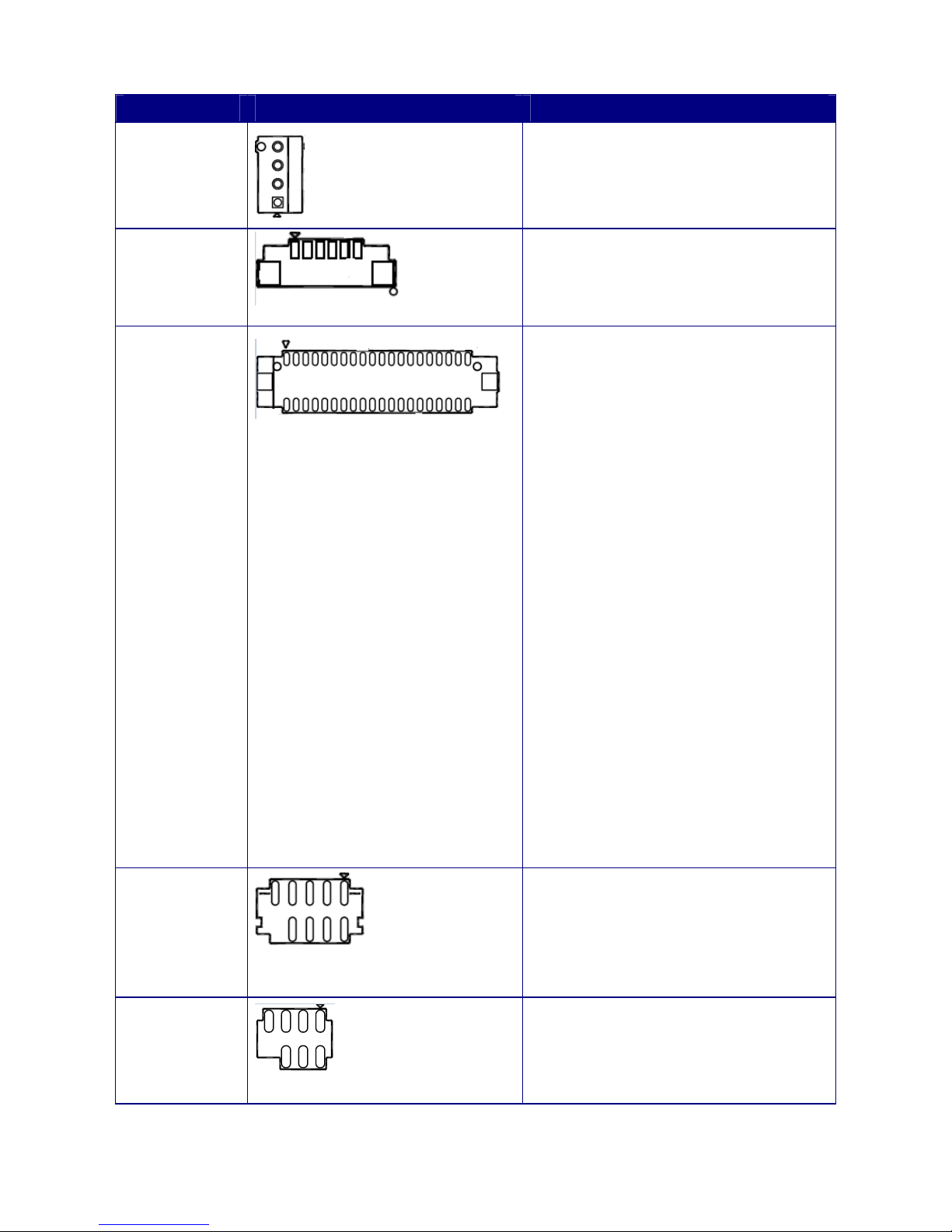
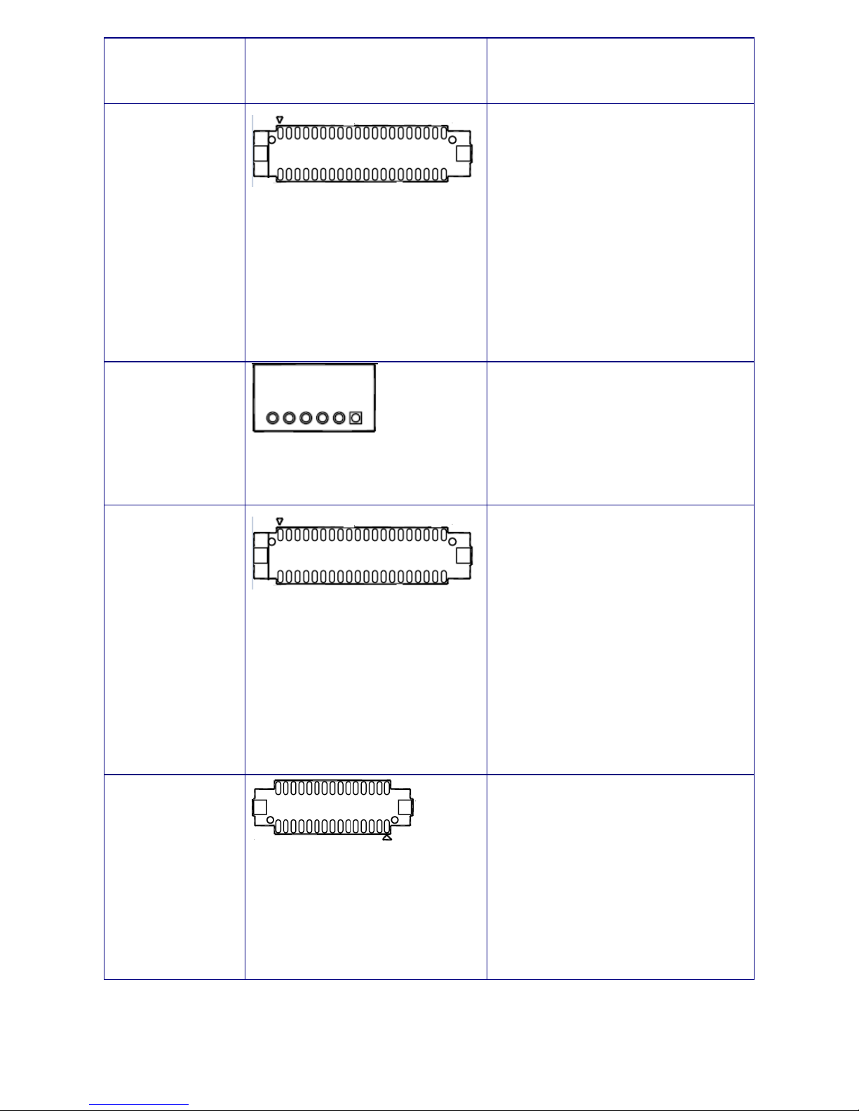
2.2.7 Daugherboard Internal Connector and PIN Definition
Label Function Note
JLED_OUT
PIN1: PLED
PIN2: SLED
JUSB2_CAMERA
PIN1: GND
PIN2: USB_HB_CM_N3
PIN3: USB_HB_CM_P3
PIN4: +5V_USB789
JUSB2_MSR
PIN1: GND
PIN2: USB_HB_CM_N2
PIN3: USB_HB_CM_P2
PIN4: +5V_USB789
COM0_OUT/
COM1_OUT
PIN1 : C1_RID#
PIN2 : No pin
PIN3 : COM1_RTS#
PIN4 : COM1_CTS#
PIN5 : GND
PIN6 : COM1_DSR#
PIN7 : COM1_TXD
PIN8 : COM1_DTR#
PIN9 : COM1_DCD#
PIN10: COM1_RXD
JLVDS_IN_30P
PIN1 : Conv_SRC PIN16 : LVDS2A_N2
PIN2 : LVDS2A_P3 PIN17 : LVDS2_VDD
PIN3 : Conv_SRC PIN8 : LVDS2A_CLK_P
PIN4 : LVDS2A_N3
PIN19 : LVDS2_VDD
PIN5 : BL_EN2 PIN20 : LVDS2A_P1
PIN6 : GND PIN21: +3.3V
PIN7 : BRIGHT2 PIN22: LVDS2A_N1
PIN8 : LVDS2A_CLK_P PIN23: GND
PIN9 : NC PIN24: GND
PIN10 : LVDS2A_CLK_N PIN25:LVDS2_EDID_DATA
Page 13
13
PIN11 : LVDS2_DETECT#_C PIN26: LVDS2A_P0
PIN12 : GND
PIN27: LVDS2_EDID_CLK
PIN13 : GND PIN28: LVDS2A_N0
PIN14 : LVDS2A_P2 PIN29: GND
PIN15 : GND PIN30: GND
JLVDS_IN_40P
PIN1 : +12V PIN21: LVDSA_N3
PIN2 : +12V PIN22: LVDSA_N2
PIN3 : LVDS1_VDD
PIN23: GND
PIN4 : +12V PIN24: GND
PIN5 : LVDS1_VDD PIN25: LVDSB_P1
PIN6 : LVDS1_VDD PIN26: LVDSB_P0
PIN7 : LVDS1_EDID_CLK PIN27: LVDSB_N1
PIN8 : LVDS1_EDID_DATA PIN28: LVDSB_N0
PIN9 : BRIGHT1 PIN29: GND
PIN10 : LVDS_VDD_EN PIN30: GND
PIN11 : BL_EN PIN31: LVDSB_P3
PIN12 : LVDS1_DETECT#_C PIN32: LVDSB_P2
PIN13 : LVDSA_P1 PIN33: LVDSB_N3
PIN14 : LVDSA_P0 PIN34: LVDSB_N2
PIN15 : LVDSA_N1 PIN35: GND
PIN16 : LVDSA_N0 PIN36: GND
PIN17 : GND PIN37: LVDSB_CLK_P
PIN18 : GND PIN38: LVDSA_CLK_P
PIN19 : LVDSA_P3 PIN39: LVDSB_CLK_N
PIN20 : LVDSA_P2 PIN40: LVDSA_CLK_N
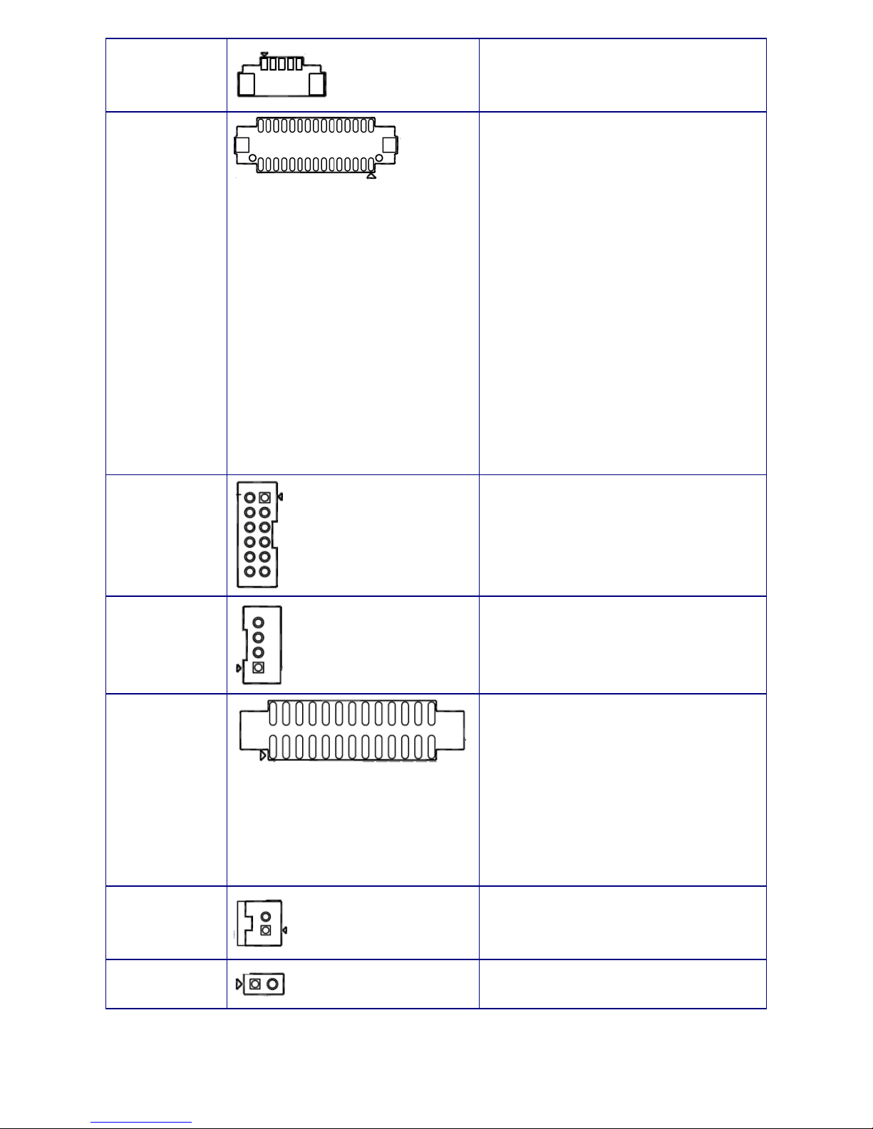
JCONV1
PIN1: Conv_SRC
PIN2: Conv_SRC
PIN3: GND
PIN4: BL_EN2
PIN5: BRIGHT2
PIN6: GND
JLVDS_OUT_40P
PIN1 : +12V PIN21: LVDSA_N3
PIN2 : +12V PIN22: LVDSA_N2
PIN3 : LVDS1_VDD
PIN23: GND
PIN4 : +12V PIN24: GND
PIN5 : LVDS1_VDD PIN25: LVDSB_P1
PIN6 : LVDS1_VDD PIN26: LVDSB_P0
PIN7 : LVDS1_EDID_CLK PIN27: LVDSB_N1
PIN8 : LVDS1_EDID_DATA PIN28: LVDSB_N0
PIN9 : BRIGHT1 PIN29: GND
PIN10 : LVDS_VDD_EN PIN30: GND
PIN11 : BL_EN PIN31: LVDSB_P3
PIN12 : LVDS1_DETECT#_C PIN32: LVDSB_P2
PIN13 : LVDSA_P1 PIN33: LVDSB_N3
PIN14 : LVDSA_P0 PIN34: LVDSB_N2
PIN15 : LVDSA_N1 PIN35: GND
PIN16 : LVDSA_N0 PIN36: GND
PIN17 : GND PIN37: LVDSB_CLK_P
PIN18 : GND PIN38: LVDSA_CLK_P
PIN19 : LVDSA_P3 PIN39: LVDSB_CLK_N
PIN20 : LVDSA_P2 PIN40: LVDSA_CLK_N
JLVDS_OUT_30P
PIN1 : Conv_SRC PIN16 : LVDS2A_N2
PIN2 : LVDS2A_P3 PIN17 : LVDS2_VDD
PIN3 : Conv_SRC PIN8 : LVDS2A_CLK_P
PIN4 : LVDS2A_N3
PIN19 : LVDS2_VDD
PIN5 : BL_EN2 PIN20 : LVDS2A_P1
PIN6 : GND PIN21: +3.3V
PIN7 : BRIGHT2 PIN22: LVDS2A_N1
PIN8 : LVDS2A_CLK_P PIN23: GND
PIN9 : NC PIN24: GND
PIN10 : LVDS2A_CLK_N PIN25:LVDS2_EDID_DATA
PIN11 : LVDS2_DETECT#_C PIN26: LVDS2A_P0
PIN12 : GND
PIN27: LVDS2_EDID_CLK
PIN13 : GND PIN28: LVDS2A_N0
PIN14 : LVDS2A_P2 PIN29: GND
PIN15 : GND PIN30: GND
Page 14
14
TOUCH2
PIN1: THY+
PIN2: THY-
PIN3: THOROBE_R
PIN4: THX-
PIN5: THX+
JUSB2_RESV
PIN1: GND
PIN2: USB_HB_CM_N4
PIN3: USB_HB_CM_P4
PIN4: +5V_USB789
JTOUCH1
PIN1 : +5V_RS232
PIN2 : +3.3V
PIN3 : 232_RX
PIN4 : 232_TX
PIN5 : GND
COM0_IN/
COM1_IN
PIN1 : COM1_DCD#
PIN2 : COM1_RXD
PIN3 : COM1_TXD
PIN4 : COM1_DTR#
PIN5 : GND
PIN6 : COM1_DSR#
PIN7 : COM1_RTS#
PIN8 : COM1_CTS#
PIN9 : C1_RID#
PIN10: No pin.
JUSB1
PIN1: USB_HB_CM_P4 PIN7: USB_HB_CM_P2
PIN2: +5V_USB789 PIN8:USB_HB_CM_P3
PIN3: USB_HB_CM_N4 PIN9 : USB_HB_CM_N2
PIN4: +5V_USB789 PIN10: USB_HB_CM_N3
PIN5: GND PIN11: +5V_USB789
PIN6: GND PIN12: +5V_USB789
JLED_IN
PIN1: PLED
PIN2: SLED
Page 15

15
3. BIOS Setup Program
This motherboard supports a programmable firmware chip that you can update using the
provided utility. Use the BIOS Setup program when you are installing a motherboard,
reconfiguring your system, or prompted to “Run Setup.” This section explains how to
configure your system using this utility.
Even if you are not prompted to use the Setup program, you can change the configuration
of your computer in the future. For example, you can enable the security password feature
or change the power management settings. This requires you to reconfigure your system
using the BIOS Setup program so that the computer can recognize these changes and
record them in the CMOS RAM of the firmware hub.
The firmware hub on the motherboard stores the Setup utility. When you start up the
computer, the system provides you with the opportunity to run this program. Press <Del>
during the Power-On-Self-Test (POST) to enter the Setup utility; otherwise, POST
continues with its test routines.
If you wish to enter Setup after POST, restart the system by pressing <Ctrl+Alt+Delete>, or
by pressing the reset button on the system chassis. You can also restart by turning the
system off and then back on. Do this last option only if the first two failed.
The Setup program is designed to make it as easy to use as possible. Being a menu-driven
program, it lets you scroll through the various sub-menus and make your selections from
the available options using the navigation keys.
The default BIOS settings for this motherboard apply for most
conditions to ensure optimum performance. If the system
becomes unstable after changing any BIOS settings, load the
default settings to ensure system compatibility and stability.
Select the Load Optimized Defaults from the BIOS menu
screen.
The BIOS setup screens shown in this section are for reference
purposes only, and may not exactly match what you see on your
screen.
Visit the system builder’s website to download the latest BIOS file
for this motherboard
Page 16

16
Legend Box
The keys in the legend bar allow you to navigate through the various setup menus
Key(s) Function Description
→← Select Screen
↑↓ Select Item
Enter Select
+ - Change Opt.
F1 General Help
F2 Previous Values
F3 Optimal Defaults
F4 Save and Exit
ESC Exit
List Box
This box appears only in the opening screen. The box displays an initial list of configurable
items in the menu you selected.
Sub-menu
Note that a right pointer symbol appears to the left of certain fields. This pointer
indicates that you can display a sub-menu from this field. A sub-menu contains additional
options for a field parameter. To display a sub-menu, move the highlight to the field and
press <Enter>. The sub-menu appears. Use the legend keys to enter values and move
from field to field within a sub-menu as you would within a menu. Use the <Esc> key to
return to the main menu.
Take some time to familiarize yourself with the legend keys and their corresponding
functions. Practice navigating through the various menus and submenus. If you
accidentally make unwanted changes to any of the fields, press <F3> to load the optimal
default values. While moving around through the Setup program, note that explanations
appear in the Item Specific Help window located to the right of each menu. This window
displays the help text for the currently highlighted field.
Page 17

17
BIOS Menu Screen
When you enter the BIOS, the following screen appears. The BIOS menu screen displays
the items that allow you to make changes to the system configuration. To access the menu
items, press the up/down/right/left arrow key on the keyboard until the desired item is
highlighted, then press [Enter] to open the specific menu.
Page 18

18
3.1 Main Setup
This menu gives you an overview of the general system specifications. The BIOS
automatically detects the items in this menu. Use this menu for basic system configurations,
such as time, date etc.
BIOS Information
Displays the auto-detected BIOS information.
System Date
The date format is <Date>,<Month>,<Day>,<Year>.
System Time
The time format is <Hour>,<Minute>,<Second>.
Page 19

19
3.2 Advanced BIOS Setup
Select the Advanced tab from the setup screen to enter the Advanced BIOS Setup screen.
You can select any of the items in the left frame of the screen, such as Chipset
configuration, to go to the sub menu for that item. You can display an Advanced BIOS
Setup option by highlighting it using the <Arrow> keys. All Advanced BIOS Setup options
are described in this section. The Advanced BIOS Setup screen is shown below. The sub
menus are described on the following pages.
Take caution when changing the settings of the Advanced menu
items. Incorrect field values can cause the system to malfunction.
Page 20

20
ACPI Settings
Enable Hibernation [Enable]
Enable or Disable system ability to hibernation.
ACPI Sleep State [S3 (Suspend to RAM)]
Select the highest ACPI sleep state the system will enter the SUSPEND button is
press. Configuration options: [Suspend Disable] [S3 (suspend to RAM )]
Page 21

21
Super IO configuration
Serial Port 1~7 Configuration
Set Parameters of Serial Port 1~7
Page 22

22
Serial Port [Enable]
Enable or Disable Serial Port
Change Settings [Auto]
Select an optimal setting for Serial Port. You can decide IO and IRQ by yourself.
Suggest to leave this option “Auto”
COM1~7 Voltage [0V]
Select 0V, 5V, 12V voltage for serial port
Parallel Port Configuration:
Parallel Port [Enable]
Enable or Disable Parallel Port (LPT/LPTE)
Change Settings [Auto]
Select an optimal setting for Parallel port device. Suggest to leave this option “Auto”
Device Mode [ STD Printer Mode]
Change the printer mode: [STD Printer Mode][SPP Mode][EPP-1.9 and SPP
Mode][ EPP-1.7 and SPP Mode][ECP Mode][ECP and EPP 1.9 Mode][ECP and EPP
1.7 Mode]
Page 23

23
CASH Drawer Voltage:
Select 0V, 12V, and 24V for cash drawer device
Cash Drawer Control in GPIO port:
Open Drawer
Write “87”h to I/O Port “2E”h
Write “87”h to I/O Port “2E”h
Write “07”h to I/O Port “2E”h
Write “07”h to I/O Port “2F”h
Write “E5”h to I/O Port “2E”h
Write “00”h to I/O Port “2F”h
Close Drawer
Write “87”h to I/O Port “2E”h
Write “87”h to I/O Port “2E”h
Write “07”h to I/O Port “2E”h
Write “07”h to I/O Port “2F”h
Write “E5”h to I/O Port “2E”h
Write “03”h to I/O Port “2F”h
Detect Drawer Satus
Write “87”h to I/O Port “2E”h
Write “87”h to I/O Port “2E”h
Page 24

24
Write “07”h to I/O Port “2E”h
Write “07”h to I/O Port “2F”h
Write “E5”h to I/O Port “2E”h
Read I/O “2F”h
Definition(bit3)
Deep Sleep Function]Disabled]:
Select to Enable/Disable Deep Sleep S5 function. When select to Enabled, Only
Power Button can power on the system
Page 25

25
PC Health Status
Display the system information including temperature and voltage.
Smart Fan Function [Enable]
Enable or Disable the Smart FAN
Smart Fan Function
When Enter this sub-menu. You can choose the mode of smart Fan.
Option:[ Manual Mode][Thermal Cruise Mode]
Page 26

26
Digital IO configuration
You can configure Digital I/O pin1~3 this this sub-menu
Case Open warning[Disable]
Enable or Disable Case Open warning
Configuration options: [Disabled] [Enabled]
Watch Dog Timer[Disable]
Enable or Disable watch dog timer function. After enabling this function, you can set
watch dog timer count mode and time out value like below.
Configuration options: [Disabled] [Enabled]
Page 27

27
S5 RTC wake up
setting
Wake system from S5 [Disable]
Enable or Disable system wake on alarm event. Select FixedTime, system will wake on
the hr :min ::sec specified.. After you enable this funciton, you can see the screen like
below.
Page 28

28
PC Health Status
Display Intel Trusted Execution Technology configuration.
Page 29

29
Display CPU information
Limit CPUID Maximum [Disable]
Disable for Windows XP
Configuration options: [Disable] [Enable]
Execute Disable Bit [Enable]
XD can prevent certain classes of malicious buffer overflow attacks when combined
with a supporting OS(Windows server 2003 SP1, WindowsXP SP2, SuSE Linux 9.2,
Redhat Enterprise 3 update 3.)
Configuration options: [Disable] [Enable]
Intel virtualization technology [Enable]
When enabled, a VMM can utilize the additional hardware capabilities provided by
Vanderpool Technology
Configuration options: [Disable] [Enable]
PPM configuration
S0ix [Enable]
Enable/Disable CPU S0ix state
Configuration options: [Disable] [Enable]
Page 30

30
IDE Configuration
Display and set IDE related device configuration.
Serial-ATA(SATA) [Enable]
nable/Disable Serial ATA
Configuration options: [Disable] [Enable]
SATA Speed Support [Gen2]
SATA speed support Gen1 or Gen2
Configuration options: [Gen1] [Gen2]
SATA mode [IDE mode]
Select IDE or AHCI
Configuration options: [IDE mode] [AHCI mode]
Serial-ATA Port1 [Enable]
Enable/Disable Serial ATA port1
Configuration options: [Enable][Disable]
Serial-ATA mSATA [Enable]
Enable/Disable Serial ATA mSATA
Configuration options: [Enable][Disable]
Page 31

31
Miscellaneous Configuration
Display miscellaneous configuration.
High Precision Timer [Enable]
Enable or Disable the High Precision Event Timer
Configuration options: [Disable] [Enable]
OS Selection[Windows 7]
OS selection
Configuration options: [Win8.X] [Windows 7]
Page 32

32
Network Stack Configuration
Network Configuration and setup
Network Stack [Enabled]
Enable/Disable UEFI Network Stack.
Configuration options: [Enabled] [Disabled]
Ipv4 PXE support [Enabled]
Enable Ipv4 PXE boot Support. If disabled, IPV4 PXE boot option will not be created.
Configuration options: [Enabled] [Disabled]
Ipv6 PXE support [Enabled]
Enable Ipv6 PXE boot Support. If disabled, IPV6 PXE boot option will not be created.
Configuration options: [Enabled] [Disabled]
PXE boot wait time
Wait time to press ESC key to abort the PXE boot
Page 33

33
Compatibility Support Module Configuration
CSM Support [Enabled]
Enable/Disable CSM Support
Configuration options: [Enable] [Disable]
GateA10 Active[Upon Request]
Upon request-GA20 can be disabled using BIOS services. Always- Do not allow
disabling GA20; this option is useful when any RT code is executed above 1MB.
Configuration options: [Upon request] [Always]
Option ROM messages[Force BIOS]
Set Display mode for option ROM
Configuration options: [Force BIOS] [Keep Current]
INT19 Trap Response[immediate]
BIOS reaction on INT19 trapping by option ROM: Immediate- execute the trap right
away; postpone- execute the trap during legacy boot.
Configuration options: [Immediate] [Postpone]
Boot option Filter[UEFI and legacy]
This option controls legacy/UEFI ROMs priority.
Configuration options: [UEFI and legacy] [legacy only]
Networks[legacy]
Controls the execution of UEFI and legacy PXE OpROM
Configuration options: [Do not launch] [UEFI][Legacy]
Page 34

34
Storage[legacy]
Controls the execution of UEFI and legacy Storage OpROM
Configuration options: [Do not launch] [UEFI][Legacy]
Video[legacy]
Controls the execution of UEFI and legacy video OpROM
Configuration options: [Do not launch] [UEFI][Legacy]
Other PCI devices[legacy]
Determine OpROM execution policy for devices other than Network, Storage, or Video
Configuration options: [UEFI][Legacy]
USB Configuration
Legacy USB Support [Enabled]
Enable Legacy USB support. Auto option disables legacy support if no USB devices
are connected. Disable option will keep USB devices available only for EFI application
Configuration options: [Enable] [Disable][Auto]
XHCI hand-off[Enable]
This is a workaround for OSes without XHCI hand-off support. The XHCI ownership
change should be claimed by XHCI driver.
Page 35

35
Configuration options: [Enable] [Disable]
EHCI hand-off[Enable]
This is a workaround for OSes without EHCI hand-off support. The EHCI ownership
change should be claimed by XHCI driver.
Configuration options: [Enable] [Disable]
USB Mass storage[Enable]
Enable/Disable USB mass storage driver support.
Configuration options: [Enable] [Disable]
USB Transfer time-out[20sec]
The time-out value for Control, bulk, and interrupt transfers.
Configuration options: [1sec] [5sec][10 sec][20sec]
Device reset time-out[20sec]
USB mass storage device start unit command time-out.
Configuration options: [10sec] [20sec][30 sec][40sec]
Device power-up delay[Auto]
Maximum time the device will take before it properly reports itself to the Host controller.
Auto’ uses default value: for a Root port it is 100ms, for a Hub port the delay is taken
from Hub descriptor.
Configuration options: [Auto] [manual]
Page 36

36
Driver healthy
Provide the Health status of the drivers and controllers.
Page 37

37
3.3 Chipset
North Bridge :
Intel IGD configuration :
Page 38

38
DVMT Pre-allocated [64MB]
Select DVMT 5.0 Pre-allocate(Fixed0 Graphic memory size used by the internal
graphic device.
Configuration options: Min: [64M] to Max:[512M]
DVMT Total Gfx Mem[256MB]
Select DVMT 5.0 Total Graphic Memory size used by the Internal Graphic device.
Configuration options: [128MB] [256MB][Max]
Aperture size[256MB]
Select the aperture size
Configuration options: [128MB] [256MB][512MB]
Page 39

39
LCD control :
Primary IGFX Boot [CRT]
Select the Video Device which will be activated during Post. This has no effect if
external graphics present. Secondary boot display selection will appear based on your
selextion. VGA modes will be supported only on primary display.
Configuration options: [VBIOS Default][CRT][eDP/LVDS1][DP/LVDS2]
Secondary IGFX Boot[eDP/LVDS1]
Select secondary display device.
Configuration options: [VBIOS Default][CRT][eDP/LVDS1][DP/LVDS2]
LVDS1 Panel Type [1024x768(24bit]]
Select the resolution of LVDS1
Configuration options: [disable]or different resolution
LVDS2 Panel Type [Disable]
Select the resolution of LVDS2
Configuration options: [disable]or different resolution
Max T0LUD
Maximum Value of T0LUD
Configuration options: [Dynamic][2GB][2.25GB][2.5GB][2.75GB][3GB]
Page 40

40
South Bridge :
Page 41

41
Azalia HD audio :
Audio Controller [Enable]
Control Detection of the Azalia device. Disabled=Azalia will be unconditionally disabled.
Enabled= Azalia will be unconditionally Enabled. Auto= Azalia will be enabled if
present disabled otherwise.
Configuration options: [Enable][Disable]
Amplifier GAIN(db)
Select Amplifier GAIN value
onfiguration options: [15.3db][21.2db][27.2db][31.8db]
Page 42

42
USB configuration :
XHCI Mode [Auto]
Mode of operation of XHCI controller
Configuration options: [Enable][Disable][Auto][Smart Auto]
USB2 Link Power[Enabled]
Enable/Disable USB2 Link Power management
Configuration options: [Enabled][Disabled]
Page 43

43
High Precision Timer [Enabled]
Enable or Disable the High precision Event Timer
Configuration options: [Enable][Disable]
Onboard LAN control[Enabled]
Enable/Disable the LAN
Configuration options: [Enabled][Disabled]
Onboard LAN BootROM[Disabled]
Enable/Disable the boot option for LAN controller
Configuration options: [Enabled][Disabled]
PCIE Wake [Disabled]
Enable or disable PCIE to wake the system from S5
Configuration options: [Enabled][Disabled]
Restore AC power loss[power off]
Select AC power state when power is re-applied after a power failure
Configuration options: [Power off][Power on][Last state]
Page 44

44
3.4 Security
Administrator Password
Set setup Administrator Password
User Password
Set User Password
Page 45

45
3.5 Boot
Setup Prompt Timeout [1]
Number of seconds to wait for setup activation key. 65535(0xFFFF) means indefinite
waiting.
Bootup NumLock State [On]
Select the keyboard NumLock state
Configuration options: [On] [Off]
Quick Boot [Disable]
Enable or disable Quick Boot option
Configuration options: [Disabled] [Enabled]
Fast Boot [Disable]
Enable or disable boot with initialization of a minimal set of devices required to launch
active boot option. Has no effect for BBS boot options.
Configuration options: [Disabled] [Enabled]
Boot mode select [LEGACY]
Select boot mode LEGACY/UEFI
Configuration options: [LEGACY] [UEFI]
Fixed boot order priorities
Define the boot priorities 1~8 in these option
Page 46

46
3.6 Save & Exit
Save changes and Exit
Exit system setup after saving the changes.
Discard changes and Exit
Exit system setup without saving the changes.
Save changes and Reset
Reset the system after saving the changes.
Discard changes and Reset
Reset the system without saving the changes.
Restore Defaults
Restore/Load default values for all the setup option.
Launch EFI shell from filesystem device
Attempts to launch EFI shell application (shell.efi) from one of the available filesystem
devices.
Page 47

47
Reset system with ME disable ModeMEUD000
ME will runs into the temporary disable mode, Ignore if ME ignition FWMEUD001.
 Loading...