

DEVICES INCORPORATED
LF3338
8-Bit Vertical Digital Image Filter
LF3338
DEVICES INCORPORATED
FEATURES DESCRIPTION
❑❑
❑ 83 MHz Data Rate
❑❑
❑❑
❑ 8-bit Data and 12-bit Coefficients
❑❑
❑❑
❑ Supports Interleaved Data Streams
❑❑
❑❑
❑ Cascadable for More Filter Taps
❑❑
❑❑
❑ Seven 3K x 8-bit, Dynamic Program-
❑❑
mable Two-Mode Line Buffers
❑❑
❑ On-board Memory for 256
❑❑
Coefficient Sets
❑❑
❑ LF Interface
❑❑
TM
Allows All 256
Coefficient Sets to be Updated
Within Vertical Blanking
❑❑
❑ Selectable 16-bit Data Output with
❑❑
User-Defined Rounding and
Limiting
❑❑
❑ Separate Input Port for Odd and
❑❑
Even Field Filtering
❑❑
❑ 8 Filter Taps
❑❑
❑❑
❑ 3.3 Volt Power Supply
❑❑
❑❑
❑ 5 Volt Tolerant I/O
❑❑
❑❑
❑ Purchase Description
❑❑
The LF3338 is a lower cost version of
the 12-bit LF3330 and is suited for
multimedia and special effects systems,
projectors, plasma display panels, scan
converters, set-top boxes, and other
consumer applications.
This device filters digital images in
the vertical dimension at real-time
video rates. Input data is 8 bits and
coefficient data is 12 bits and both are
in two’s complement format. The
output is also in two’s complement
format and may be rounded to 16 bits.
The filter is an 8-tap FIR filter with all
required line buffers contained onchip. The line buffers can store video
lines with lengths from 4 to 3076
pixels. Multiple LF3338s can be
cascaded together to create larger
vertical filters.
8-Bit Vertical Digital Image Filter
Due to the length of the line buffers,
interleaved data can be fed directly
into the device and filtered without
separating the data into individual
data streams. The number of interleaved data sets that the device can
handle is limited only by the length of
the on-chip line buffers. If the interleaved video line has 3076 data values
or less, the filter can handle it.
The LF3338 contains enough on-board
memory to store 256 coefficient sets.
The LF InterfaceTM allows all 256
coefficient sets to be updated within
vertical blanking.
Selectable 16-bit data output with
user-defined rounding and limiting
minimizes the constraints put on
coefficient sets for various filter
implementations.
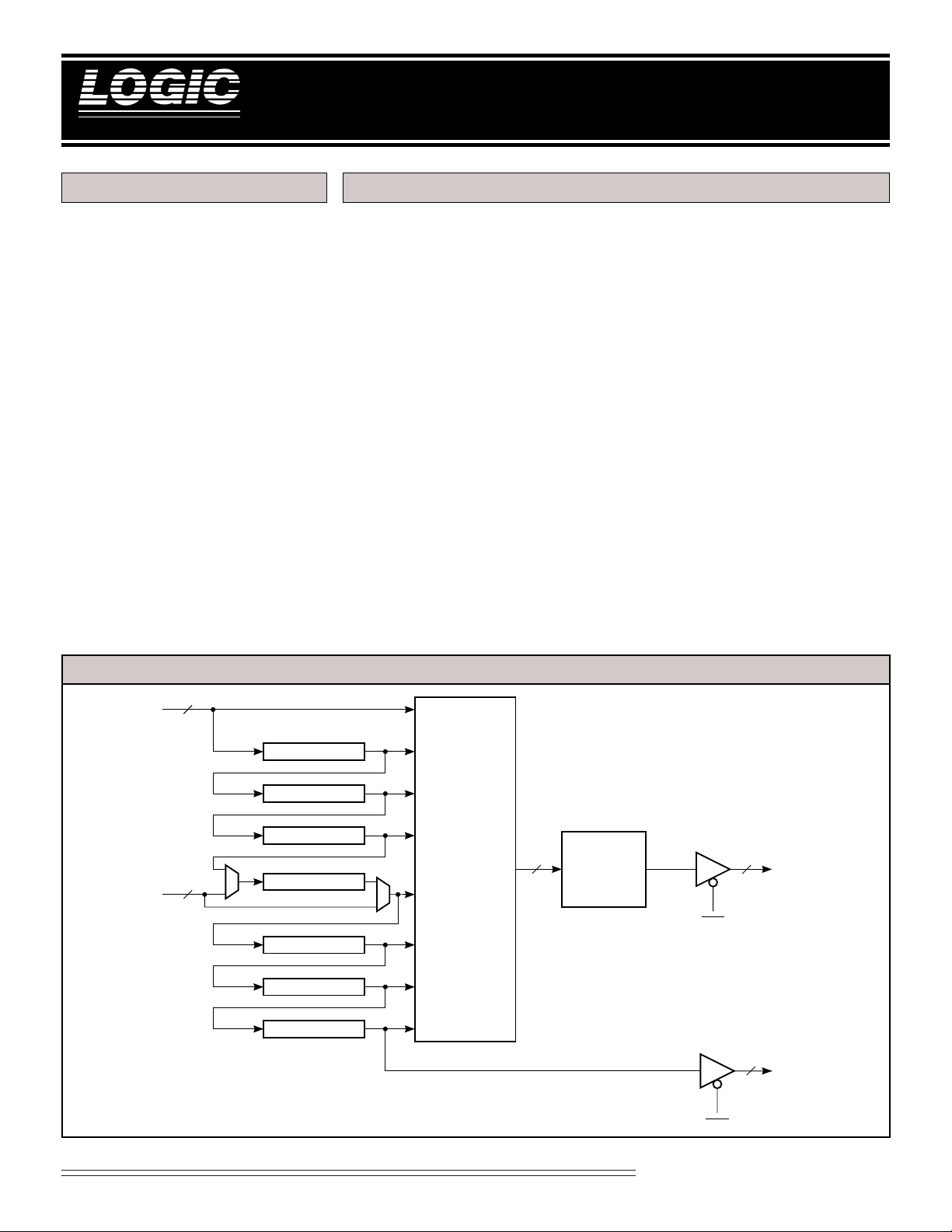
LF3338 BLOCK DIAGRAM
DIN
VB
8
7-0
8
7-0
3K LINE BUFFER
3K LINE BUFFER
3K LINE BUFFER
3K LINE BUFFER
3K LINE BUFFER
3K LINE BUFFER
3K LINE BUFFER
32
8-TAP VERTICAL FILTER
256 COEFFICIENT SET STORAGE
ROUND
SELECT
LIMIT
CIRCUITRY
OED
16
15-0
DOUT
8
COUT
7-0
OEC
Video Imaging Products
1
04/06/1999–LDS.3338-B
DEVICES INCORPORATED
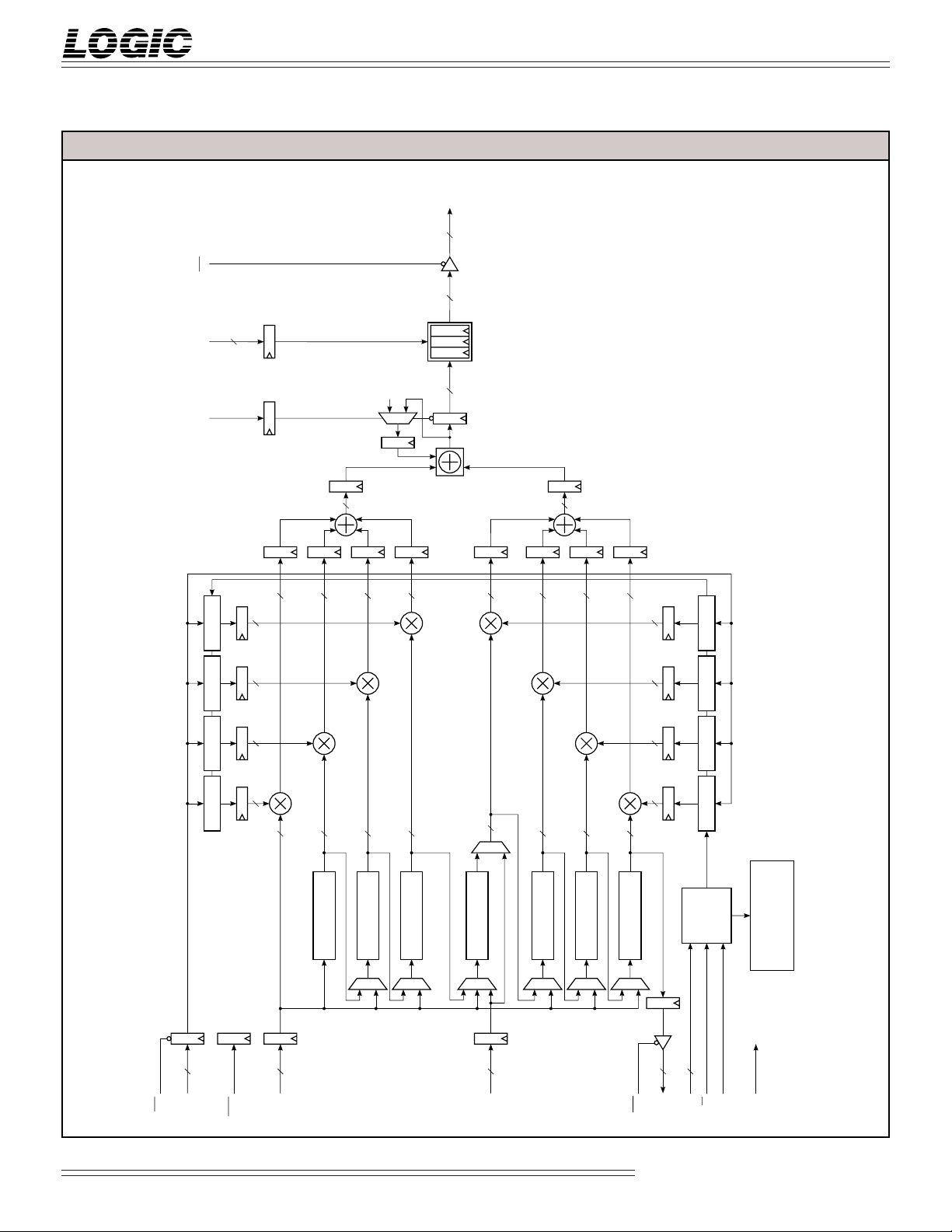
FIGURE 1. LF3338 FUNCTIONAL BLOCK DIAGRAM
OED
3-0
4
RSL
16
16
15-0
DOUT
LIMIT
SELECT
ROUND
LF3338
8-Bit Ver tical Digital Image Filter
ACC
Coef Bank 6 Coef Bank 5 Coef Bank 4
Coef Bank 7
"0"
22
20
20
20
12 12 12 12
8
8
8
32
22
20
8
20
8
20
20
20
12 12 12 12
8
8
8
Coef Bank 0 Coef Bank 1 Coef Bank 2 Coef Bank 3
CEN
LF
12
11-0
CF
INTERFACE
LD
PAUSE
CONFIGURATION AND
CONTROL REGISTERS
CLK
3K Line Buffer
3K Line Buffer
3K Line Buffer
SHEN
8
7-0
DIN
8
7-0
CA
3K Line Buffer
8
7-0
VB
3K Line Buffer
3K Line Buffer
3K Line Buffer
8
7-0
OEC
COUT
Video Imaging Products
2
04/06/1999–LDS.3338-B
DEVICES INCORPORATED
765 210
–2
7
(Sign)
262
5
22212
0
11 10 9 2 1 0
–2
0
(Sign)
2–12
–2
2–92
–102–11
Input Data Coefficient Data
LF3338
8-Bit Vertical Digital Image Filter
SIGNAL DEFINITIONS
Power
VCC and GND
+3.3 V power supply. All pins must be
connected.
Clock
CLK — Master Clock
The rising edge of CLK strobes all
enabled registers.
Inputs
DIN7-0 — Data Input
DIN7-0 is the 8-bit registered data input
port. Data is latched on the rising edge
of CLK.
VB7-0 — Field Filtering Data Input
VB7-0 is the 8-bit registered data input
port used only when implementing
Odd and Even Field Filtering (see
Functional Description section for a full
discussion). Data is latched on the
rising edge of CLK.
CF11-0 — Coefficient Input
CF11-0 is used to load data into the
coefficient banks and configuration/
control registers. Data present on
CF11-0 is latched into the LF Interface
on the rising edge of CLK when LD is
LOW (see the LF InterfaceTM section for
a full discussion).
CA7-0 — Coefficient Address
CA7-0 determines which row of data in
the coefficient banks is fed to the
multipliers. CA7-0 is latched into the
Coefficient Address Register on the
rising edge of CLK when CEN is LOW.
Outputs
DOUT15-0 — Data Output
DOUT15-0 is the 16-bit registered data
output port.
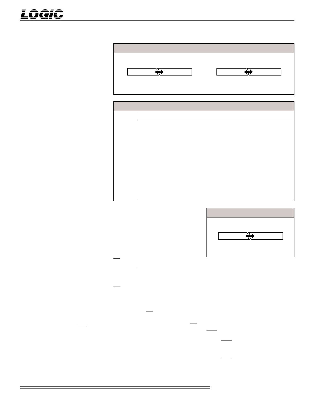
FIGURE 2. INPUT FORMATS
TABLE 1. OUTPUT FORMATS
SLCT4-0 S15 S14 S13 · · · S8 S7 · · · S2 S1 S0
00000 F15 F14 F13 · · · F8 F7 · · · F2 F1 F0
00001 F16 F15 F14 · · · F9 F8 · · · F3 F2 F1
00010 F17 F16 F15 · · · F10 F9 · · · F4 F3 F2
· ··· ·· ···
· ··· ·· ···
· ··· ·· ···
01110 F29 F28 F27 · · · F22 F21 · · · F16 F15 F14
01111 F30 F29 F28 · · · F23 F22 · · · F17 F16 F15
10000 F31 F30 F29 · · · F24 F23 · · · F18 F17 F16
COUT7-0 — Cascade Data Output
COUT7-0 is a 8-bit cascade output
port. COUT7-0 on one device
should be connected to DIN7-0 of
another LF3338.
Controls
TM
LD — Coefficient Load
When LD is LOW, data on CF11-0
is latched into the LF Interface
TM
on the rising edge of CLK. When
LD is HIGH, data can not be
latched into the LF InterfaceTM.
When enabling the LF Interface
TM
for data input, a HIGH to LOW
transition of LD is required in
order for the input circuitry to
function properly. Therefore, LD
must be set HIGH immediately
after power up to ensure proper
operation of the input circuitry
(see the LF InterfaceTM section for
a full discussion).
3
FIGURE 3. ACCUMULATOR FORMAT
Accumulator Output
31 30 29 2 1 0
16
–2
(Sign)
2152
14
–132–142–15
2
PAUSE — LF InterfaceTM Pause
When PAUSE is HIGH, the LF
InterfaceTM loading sequence is halted
until PAUSE is returned to a LOW
state. This effectively allows the user
to load coefficients and control
registers at a slower rate than the
master clock (see the LF Interface
TM
section for a full discussion).
CEN — Coefficient Address Enable
When CEN is LOW, data on CA7-0 is
latched into the Coefficient Address
Register on the rising edge of CLK.
When CEN is HIGH, data on CA7-0 is
not latched and the register’s contents
will not be changed.
Video Imaging Products
04/06/1999–LDS.3338-B
DEVICES INCORPORATED
LF3338
8-Bit Ver tical Digital Image Filter
TABLE 2. CONFIGURATION REGISTER 0 – ADDRESS 200H
BITS FUNCTION DESCRIPTION
11-0 Line Buffer Length See Line Buffer Description Section
TABLE 3. CONFIGURATION REGISTER 1 – ADDRESS 201H
BITS FUNCTION DESCRIPTION
0 Line Buffer Mode 0: Delay Mode
1: Recirculate Mode
1 Line Buffer Load 0: Normal Load
1: Parallel Load
2 Odd and Even Field 0: VB Port Disabled
Filtering Port Enable 1: VB Port Enabled
3 Odd and Even Field 0: VB Line Buffer Disabled
Filtering Line Buffer Enable 1: VB Line Buffer Enabled
11-4 Reserved Must be set to “0”
TABLE 4. CONFIGURATION REGISTER 2 – ADDRESS 202H
BITS FUNCTION DESCRIPTION
0 Limit Enable 0: Limiting Disabled
1: Limiting Enabled
11-1 Reserved Must be set to “0”
FIGURE 4. RSL CIRCUITRY
RSL
3-0
4
R0R15
S0S15
L0L15
DATA IN
32
32
RND
32
5
SELECT
16
32
LIMIT
TABLE 5. CONFIGURATION REGISTER 3 – ADDRESS 203H
BITS FUNCTION DESCRIPTION
0 Cascade Mode 0: First Device
1: Cascaded Device
11-1 Reserved Must be set to “0”
ACC — Accumulator Control
When ACC is HIGH, the accumulator
is enabled for accumulation and the
accumulator output register is
disabled for loading. When ACC is
LOW, no accumulation is performed
and the accumulator output register
is enabled for loading. ACC is
latched on the rising edge of CLK.
SHEN — Shift Enable
SHEN enables or disables the
loading of data into the input/
cascade registers and the line
buffers. When SHEN is LOW, data
is loaded into the input/cascade
registers and shifted through the
line buffers on the rising edge of
CLK. When SHEN is HIGH, data
can not be loaded into the input/
cascade registers or shifted through
the line buffers and their contents
will not be changed.
RSL3-0 — Round/Select/Limit Control
RSL3-0 determines which of the
sixteen user-programmable round/
select/limit registers are used in the
round/select/limit circuitry. A
value of 0 on RSL3-0 selects round/
select/limit register 0. A value of 1
selects round/select/limit register 1
and so on. RSL3-0 is latched on the
RSL CIRCUITRY
16
DATA OUT
rising edge of CLK (see the round,
select, and limit sections for a
complete discussion).
OED — DOUT Output Enable
When OED is LOW, DOUT15-0 is
enabled for output. When OED is
HIGH, DOUT15-0 is placed in a
high-impedance state.
OEC — COUT Output Enable
When OEC is LOW, COUT7-0 is
enabled for output. When OEC is
HIGH, COUT7-0 is placed in a highimpedance state.
Video Imaging Products
4
04/06/1999–LDS.3338-B
DEVICES INCORPORATED
LF3338
8-Bit Vertical Digital Image Filter
FUNCTIONAL DESCRIPTION
Line Buffers
The maximum delay length of each line
buffer is 3076 cycles and the minimum
is 4 cycles. Configuration Register 0
(CR0) determines the delay length of
the line buffers. The line buffer length
is equal to the value of CR0 plus 4. A
value of 0 for CR0 sets the line buffer
length to 4. A value of 3072 for CR0
sets the line buffer length to 3076. Any
values for CR0 greater than 3072 are not
valid.
The line buffers have two modes of
operation: delay mode and recirculate
mode. Bit 0 of Configuration Register 1
determines which mode the line buffers
are in. In delay mode, the data input to
the line buffer is delayed by an amount
determined by CR0. In recirculate
mode, the output of the line buffer is
routed back to the input of the line
buffer allowing the line buffer contents
to be read multiple times.
Bit 1 of Configuration Register 1 allows
the line buffers to be loaded in parallel.
When Bit 1 is “1”, the input register
(DIN7-0) loads all seven line buffers in
parallel. This allows all the line buffers
to be preloaded with data in the
amount of time it normally takes to
load a single line buffer.
Odd and Even Field Filtering
The LF3338 is capable of odd and even
field filtering. Bit 2 of Configuration
Register 1 enables the VB Data Input
port required for odd and even field
filtering. Bit 3 of the same configuration register enables the line buffer in
the VB Data path. Line buffer length is
set to the length written to Configuration Register 0. If line buffer parallel
load is enabled and odd and even field
filtering is enabled, the data for the VB
line buffer comes from the VB Data
Input port.
Interleaved Data
The LF3338 is capable of handling
interleaved data. The number of data
sets it can handle is determined by the
number of data values contained in a
video line. If the interleaved video line
has 3076 data values or less, the LF3338
can handle it no matter how many data
sets are interleaved together.
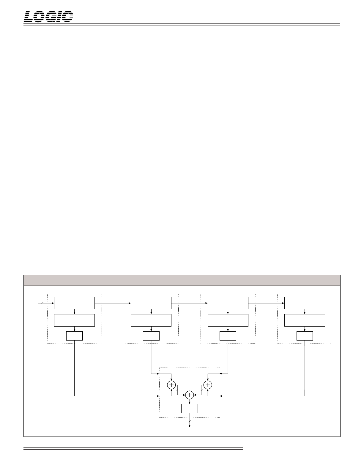
Cascading
A cascade port is provided to allow
cascading of multiple devices for
more filter taps (see Figure 5).
COUT7-0 of one device should be
connected to DIN7-0 of another
device. As many LF3338s as desired
may be cascaded together. However, the outputs of the LF3338s
must be added together with external adders.
The first line buffer on a cascaded
device must have its length shortened by two delays. This is to
account for the added delays of the
input register on the device and the
cascade output register from the
previous LF3338. If Bit 0 of Configuration Register 3 is set to “1”,
the length of the first line buffer will
be reduced by two. This will make
its effective length the same as the
other line buffers on the device. If
Bit 0 of Configuration Register 3 is
set to “0”, the length of the first line
buffer will be the same as the other
line buffers. When cascading
devices, the first LF3338 should
have Bit 0 of Configuration Register
FIGURE 5. MULTIPLE LF3338S CASCADED TOGETHER
8
DIN LINE BUFFERS
VERTICAL FILTER
RSL
CIRCUIT
COUT DIN
LINE BUFFERS LINE BUFFERS LINE BUFFERS
VERTICAL FILTER VERTICAL FILTER VERTICAL FILTER
RSL
CIRCUIT
COUT
LF3347
29 TAP RESULT
5
LF3338LF3338LF3338
DIN DIN
RSL
CIRCUIT
2525
RSL
CIRCUIT
16
DATA OUT
Video Imaging Products
COUT
LF3338
RSL
CIRCUIT
04/06/1999–LDS.3338-B

DEVICES INCORPORATED
LF3338
8-Bit Ver tical Digital Image Filter
3 set to “0”. Any LF3338s cascaded
after the first LF3338 should have
Bit 0 of Configuration Register 3 set
to “1”. When not cascading, Bit 0 of
Configuration Register 3 should be
set to “0”.
It is important to note that the first
multiplier on all cascaded devices
should not be used. This is because
the first multiplier does not have a
line buffer in front of it. The coefficient value sent to the first multiplier on a cascaded device should be
“0”.
programmable. This allows the filter’s
output to be rounded to any precision
required. Since any 32-bit value may
be programmed into the round
registers, the device can support
complex rounding algorithms as well
as standard half-LSB rounding. RSL3-0
determines which of the sixteen round
registers are used in the rounding
operation. A value of 0 on RSL3-0
selects round register 0. A value of 1
selects round register 1 and so on.
RSL3-0 may be changed every clock
cycle if desired. This allows the
rounding algorithm to be changed
every clock cycle. This is useful when
Rounding
The filter output may be rounded by
adding the contents of one of the
sixteen round registers to the filter
output (see Figure 4). Each round
register is 32 bits wide and user-
filtering interleaved data. If rounding
is not desired, a round register should
be loaded with 0 and selected as the
register used for rounding. Round
register loading is discussed in the
LF InterfaceTM section.
FIGURE 6. COEFFICIENT BANK LOADING SEQUENCE
Output Select
The word width of the filter output
is 32 bits. However, only 16 bits
may be sent to DOUT15-0. The select
circuitry determines which 16 bits
are passed (see Table 1). There are
sixteen select registers which control
the select circuitry. Each select
register is 5 bits wide and userprogrammable. RSL3-0 determines
which of the sixteen select registers
are used in the select circuitry.
Select register 0 is chosen by loading
a 0 on RSL3-0. Select register 1 is
chosen by loading a 1 on RSL3-0 and
so on. RSL3-0 may be changed every
clock cycle if desired. This allows
the 16-bit window to be changed
every clock cycle. This is useful
when filtering interleaved data.
Select register loading is discussed
in the LF InterfaceTM section.
COEFFICIENT SET 1 COEFFICIENT SET 2 COEFFICIENT SET 3
CLK
W1
LD
CF
11-0
W1: Coefficient Set 1 written to coefficient banks during this clock cycle.
W2: Coefficient Set 2 written to coefficient banks during this clock cycle.
W3: Coefficient Set 3 written to coefficient banks during this clock cycle.
ADDR1COEF
0
COEF7ADDR2COEF
0
COEF7ADDR3COEF
FIGURE 7. CONFIGURATION/CONTROL REGISTER LOADING SEQUENCE
CONFIG REG ROUND REGISTER LIMIT REGISTER
CLK
LD
CF
11-0
W1: Configuration Register loaded with new data on this rising clock edge.
W2: Select Register loaded with new data on this rising clock edge.
W3: Round Register loaded with new data on this rising clock edge.
W4: Limit Register loaded with new data on this rising clock edge.
ADDR1 DATA1 ADDR3 DATA4
SELECT REG
W1
2 DATA1
ADDR
W2
W3 W4
1 DATA3DATA2 ADDR4 DATA2DATA1
DATA
W2 W3
0
COEF
DATA4DATA3
7
Video Imaging Products
6
04/06/1999–LDS.3338-B

DEVICES INCORPORATED
LF3338
8-Bit Vertical Digital Image Filter
Limiting
An output limiting function is
provided for the output of the
filter. The limit registers determine the valid range of output
values when limiting is enabled
(Bit 0 in Configuration Register 2).
There are sixteen 32-bit limit
registers. RSL3-0 determines
which limit register is used during
the limit operation. A value of 0
on RSL3-0 selects limit register 0.
A value of 1 selects limit register 1
and so on. Each limit register
contains both an upper and lower
limit value. If the value fed to the
limiting circuitry is less than the
lower limit, the lower limit value
is passed as the filter output. If
the value fed to the limiting
circuitry is greater than the upper
limit, the upper limit value is
passed as the filter output. RSL3-0
may be changed every clock cycle
if desired. This allows the limit
range to be changed every clock
cycle. This is useful when filtering
interleaved data. When loading
limit values into the device, the
upper limit must be greater than
the lower limit. Limit register
loading is discussed in the LF
InterfaceTM section.
Coefficient Banks
The coefficient banks store the
coefficients which feed into the
multipliers in the filter. There is a
separate bank for each multiplier.
Each bank can hold 256 12-bit
coefficients. The banks are loaded
using the LF InterfaceTM. Coefficient
bank loading is discussed in the
LF InterfaceTM section.
Configuration and Control Registers
The configuration registers determine how the LF3338 operates.
Tables 2 through 5 show the formats
of the four configuration registers.
There are three types of control
registers: round, select, and limit.
There are sixteen round registers.
Each round register is 32 bits wide.
RSL3-0 determines which round
register is used for rounding.
There are sixteen select registers.
Each select register is 5 bits wide.
RSL3-0 determines which select
register is used for the select circuitry.
There are sixteen limit registers.
Each limit register is 32 bits wide
and stores both an upper and lower
limit value. The lower limit is
stored in bits 15-0 and the upper
FIGURE 8. COEFFICIENT BANK LOADING SEQUENCE WITH PAUSE IMPLEMENTATION
COEFFICIENT SET 1
CLK
PAUSE
LD
CF
11-0
W1: Configuration Register loaded with new data on this rising clock edge.
ADDR
1
COEF
0
COEF
1
COEF
7
FIGURE 9. CONFIGURATION AND SELECT REGISTER LOADING SEQUENCE WITH PAUSE IMPLEMENTATION
CLK
PAUSE
LD
11-0
CF
CONFIGURATION REGISTER
ADDR
1
DATA
W1
1
ADDR
SELECT REGISTER
2
DATA
W2
1
W1
W1: Configuration Register loaded with new data on this rising clock edge.
W2: Select Register loaded with new data on this rising clock edge.
7
Video Imaging Products
04/06/1999–LDS.3338-B

DEVICES INCORPORATED
LF3338
8-Bit Ver tical Digital Image Filter
limit is stored in bits 31-16. RSL3-0
determines which limit register is
used for limiting when limiting is
enabled. Configuration and control
register loading is discussed in the
LF InterfaceTM section.
LF Interface
The LF InterfaceTM is used to load
data into the coefficient banks and
configuration/control registers. LD
is used to enable and disable the
TM
LF InterfaceTM. When LD goes LOW,
the LF InterfaceTM is enabled for data
input. The first value fed into the
interface on CF11-0 is an address
which determines what the interface
is going to load. The three most
FIGURE 10. ROUND REGISTER LOADING SEQUENCE WITH PAUSE IMPLEMENTATION
ROUND REGISTER
CLK
PAUSE
LD
ADDR
11-0
CF
W1: Round Register loaded with new data on this rising clock edge.
1
DATA
1
DATA
2
DATA
3
FIGURE 11. LIMIT REGISTER LOADING SEQUENCE WITH PAUSE IMPLEMENTATION
DATA
W1
4
LIMIT REGISTER
CLK
W1
PAUSE
LD
CF
11-0
W1: Limit Register loaded with new data on this rising clock edge.
ADDR
1
DATA
1
DATA
2
DATA
3
DATA
4
TABLE 10. COEFFICIENT BANK LOADING FORMAT
CF11 CF10 CF9 CF8 CF7 CF6 CF5 CF4 CF3 CF2 CF1 CF0
1st Word - Address 0 0 0000001010
2nd Word - Bank 0 0 0 1000010000
3rd Word - Bank 1 0 1 0101000011
4th Word - Bank 2 1 1 0001110110
5th Word - Bank 3 1 0 0111100011
6th Word - Bank 4 0 1 1100000001
7th Word - Bank 5 1 0 0000110010
8th Word - Bank 6 1 1 1100100000
9th Word - Bank 7 0 0 0101000011
Video Imaging Products
8
04/06/1999–LDS.3338-B

DEVICES INCORPORATED
LF3338
8-Bit Vertical Digital Image Filter
significant bits (CF11-9) determine if
the LF InterfaceTM will load coefficient
banks or configuration/control
registers (see Table 6). The nine least
significant bits (CF8-0) are the address
for whatever is to be loaded (see
Tables 7 through 9). For example, to
load address 15 of the coefficient
banks, the first data value into the
LF InterfaceTM should be 00FH. To
load limit register 10, the first data
value should be E0AH. The first
address value should be loaded into
the interface on the same clock cycle
that latches the HIGH to LOW
transition of LD (see Figures 6 and 7).
The next value(s) loaded into the
interface are the data value(s) which
will be stored in the bank or register
defined by the address value. When
loading coefficient banks, the interface
will expect eight values to be loaded
into the device after the address value.
The eight values are coefficients 0
through 7. When loading configuration or select registers, the interface
will expect one value after the address
value. When loading round or limit
registers, the interface will expect four
TABLE 6. CF11-9 DECODE
11 10 9 DESCRIPTION
0 0 0 Coefficient Banks
0 0 1 Configuration Registers
0 1 1 Select Registers
1 0 1 Round Registers
1 1 1 Limit Registers
values after the address value. Figures 6 and 7 show the data loading
sequences for the coefficient banks
and configuration/control registers.
PAUSE allows the user to effectively
slow the rate of data loading through
the LF InterfaceTM. When PAUSE is
HIGH, the LF InterfaceTM is held until
PAUSE is returned to a LOW. Figures
8 through 11 display the effects of
PAUSE while leading coefficient and
control data.
Table 10 shows an example of
loading data into the coefficient
banks. The following data values
are written into address 10 of
coefficient banks 0 through 7: 210H,
543H, C76H, 9E3H, 701H, 832H,
F20H, 143H. Table 11 shows an
example of loading data into a
TABLE 7. ROUND REGISTERS
REGISTER ADDRESS (HEX)
0 A00
1 A01
14 A0E
15 A0F
TABLE 8. SELECT REGISTERS
REGISTER ADDRESS (HEX)
0 600
1 601
14 60E
15 60F
TABLE 9. LIMIT REGISTERS
REGISTER ADDRESS (HEX)
0 E00
1 E01
14 E0E
15 E0F
TABLE 11. CONFIGURATION REGISTER LOADING FORMAT
CF11 CF10 CF9 CF8 CF7 CF6 CF5 CF4 CF3 CF2 CF1 CF0
1st Word - Address 0 0 1000000010
2nd Word - Data 0 0 0000000011
TABLE 12. ROUND REGISTER LOADING FORMAT
CF11 CF10 CF9 CF8 CF7 CF6 CF5 CF4 CF3 CF2 CF1 CF0
1st Word - Address 1 0 1000001100
2nd Word- Data R RRR10100010*
3rd Word - Data R RRR11110100
4th Word - Data R RRR10000011
5th Word - Data R RRR0**1110110
R = Reserved. Must be set to “0”.
* This bit represents the LSB of the Round Register.
** This bit represents the MSB of the Round Register.
Video Imaging Products
9
04/06/1999–LDS.3338-B

DEVICES INCORPORATED
LF3338
8-Bit Ver tical Digital Image Filter
configuration register. Data value
003H is written into Configuration
Register 2. Table 12 shows an
example of loading data into a
round register. Data value
7683F4A2H is written into round
register 12. Table 13 shows an
example of loading data into a select
register. Data value 00FH is loaded
into select register 2. Table 14
shows an example of loading data
into limit register 7. Data value
3B60H is loaded as the lower limit
and 72A4H is loaded as the upper
limit.
It takes 9S clock cycles to load S
coefficient sets into the device. Therefore, it takes 2304 clock cycles to load
all 256 coefficient sets. Assuming an
83 MHz clock rate, all 256 coefficient
sets can be updated in less than 27.7 µs,
which is well within vertical blanking
time. It takes 5S clock cycles to load S
round or limit registers. Therefore, it
takes 160 clock cycles to update all
round and limit registers. Assuming an
83 MHz clock rate, all round/limit
registers can be updated in 1.92 µs.
The coefficient banks and configuration/control registers are not loaded
with data until all data values for
the specified address are loaded into
the LF InterfaceTM. In other words,
the coefficient banks are not written
to until all eight coefficients have
been loaded into the LF InterfaceTM.
A round register is not written to
until all four data values are loaded.
After the last data value is loaded,
the interface will expect a new
address value on the next clock
cycle. After the next address value
is loaded, data loading will begin
again as previously discussed. As
long as data is loaded into the
interface, LD must remain LOW.
After all desired coefficient banks
and configuration/control registers
are loaded with data, the LF
InterfaceTM must be disabled. This is
done by setting LD HIGH on the clock
cycle after the clock cycle which
latches the last data value. It is
important that the LF Interface
TM
remain disabled when not loading
data into it.
TABLE 13. SELECT REGISTER LOADING FORMAT
CF11 CF10 CF9 CF8 CF7 CF6 CF5 CF4 CF3 CF2 CF1 CF0
1st Word - Address 0 1 1000000010
2nd Word - Data 0 0 0000001111
TABLE 14. LIMIT REGISTER LOADING FORMAT
CF11 CF10 CF9 CF8 CF7 CF6 CF5 CF4 CF3 CF2 CF1 CF0
1st Word - Address 1 1 1000000111
2nd Word- Data R RRR01100000
3rd Word - Data R RRR0*0111011
4th Word - Data R RRR10100100
5th Word - Data R RRR0**1110010
R = Reserved. Must be set to “0”.
* This bit represents the MSB of the Lower Limit.
** This bit represents the MSB of the Upper Limit.
Video Imaging Products
10
04/06/1999–LDS.3338-B

DEVICES INCORPORATED
LF3338
8-Bit Vertical Digital Image Filter
MAXIMUM RATINGS
Storage temperature ........................................................................................................... –65°C to +150°C
Operating ambient temperature........................................................................................... –55°C to +125°C
VCC supply voltage with respect to ground............................................................................ –0.5 V to +4.5V
Input signal with respect to ground .......................................................................................... –0.5 V to 5.5 V
Signal applied to high impedance output ................................................................................. –0.5 V to 5.5 V
Output current into low outputs............................................................................................................. 25 mA
Latchup current ............................................................................................................................... > 400 mA
ESD Classification (MIL-STD-883E METHOD 3015.7) ...................................................................... Class 3
OPERATING CONDITIONS
Active Operation, Commercial 0°C to +70°C 3.00 V ≤ VCC ≤ 3.60 V
Active Operation, Military –55°C to +125°C 3.00 V ≤ VCC ≤ 3.60V
Above which useful life may be impaired (Notes 1, 2, 3, 8)
To meet specified electrical and switching characteristics
Mode Temperature Range (Ambient) Supply Voltage
ELECTRICAL CHARACTERISTICS
Symbol Parameter Test Condition Min Typ Max Unit
VOH Output High Voltage VCC = Min., IOH = –4 mA 2.4 V
VOL Output Low Voltage VCC = Min., IOL = 8.0 mA 0.4 V
VIH Input High Voltage 2.0 5.5 V
VIL Input Low Voltage (Note 3) 0.0 0.8 V
IIX Input Current Ground ≤ VIN ≤ VCC (Note 12) ±10 µA
IOZ Output Leakage Current Ground ≤ VOUT ≤ VCC (Note 12) ±10 µA
ICC1 VCC Current, Dynamic (Notes 5, 6) 120 mA
ICC2 VCC Current, Quiescent (Note 7) 1mA
CIN Input Capacitance TA = 25°C, f = 1 MHz 10 pF
COUT Output Capacitance TA = 25°C, f = 1 MHz 1 0 pF
Over Operating Conditions (Note 4)
Video Imaging Products
11
04/06/1999–LDS.3338-B

DEVICES INCORPORATED
SWITCHING CHARACTERISTICS
LF3338
8-Bit Ver tical Digital Image Filter
COMMERCIAL OPERATING RANGE (0°C to +70°C)
Notes 9, 10 (ns)
LF3338–
12
Symbol Parameter Min Max
tCYC Clock Cycle Time 12
tPW Clock Pulse Width 5
tS Input Setup Time 4
tH Input Hold Time 0.5
tDD Data Output Delay 8
tDC Cascade Data Output Delay 9
tDIS Three-State Output Disable Delay (Note 11) 10
tENA Three-State Output Enable Delay (Note 11) 10
SWITCHING WAVEFORMS:DATA I/O
CLK
DIN
7-0
CA7-0 CAN CAN+1
123456
tH
tS
DINN DINN+1
tPW
tCYC
tPW
7
VB7-0
CONTROLS
(Except OE)
OE
DOUT
15-0
COUT7-0
VBN VBN+1
tENA
HIGH IMPEDANCE
HIGH IMPEDANCE
tDDtDIS
DOUTN-1
tDC
N-1 COUTN
COUT
DOUTN
Video Imaging Products
12
04/06/1999–LDS.3338-B

DEVICES INCORPORATED
LF3338
8-Bit Vertical Digital Image Filter
COMMERCIAL OPERATING RANGE (0°C to +70°C)
Notes 9, 10 (ns) VALUES NOT VALID
LF3338–
12
Symbol Parameter Min Max
tCFS Coefficient Input Setup Time 5
tCFH Coefficient Input Hold Time 0
tLS Load Setup Time 4
tLH Load Hold Time 0
tPS PAUSE Setup Time 4
tPH PAUSE Hold Time 0.5
SWITCHING WAVEFORMS: LF INTERFACE
CLK
t
LS
LD
PAUSE
t
CF
11–0 CF
CFS
12 453
t
ADDRESS
PW
t
CFH
t
CYC
CF
t
PW
0
TM
6
t
LH
t
PS
t
PH
CF
1
2
Video Imaging Products
13
04/06/1999–LDS.3338-B

DEVICES INCORPORATED
OE
0.2 V
t
DIS
t
ENA
0.2 V
1.5 V 1.5 V
3.0V Vth
1
Z
0
Z
Z
1
Z
0
1.5 V
1.5 V
0V Vth
VOL*
V
OH
*
V
OL
*
V
OH
*
Measured V
OL
with IOH = –10mA and IOL = 10mA
Measured V
OH
with IOH = –10mA and IOL = 10mA
NOTES
LF3338
8-Bit Ver tical Digital Image Filter
1. Maximum Ratings indicate stress
specifications only. Functional operation of these products at values beyond
those indicated in the Operating Conditions table is not implied. Exposure to
maximum rating conditions for extended periods may affect reliability.
2. The products described by this specification include internal circuitry designed to protect the chip from damaging substrate injection currents and accumulations of static charge. Nevertheless, conventional precautions
should be observed during storage,
handling, and use of these circuits in
order to avoid exposure to excessive
electrical stress values.
3. This device provides hard clamping
of transient undershoot. Input levels
below ground will be clamped beginning at –0.6 V. The device can withstand indefinite operation with inputs
or outputs in the range of –0.5 V to
+5.5 V. Device operation will not be
adversely affected, however, input current levels will be well in excess of 100
mA.
9. AC specifications are tested with
input transition times less than 3 ns,
output reference levels of 1.5 V (except
tDIS test), and input levels of nominally
0 to 3.0 V. Output loading may be a
resistive divider which provides for
specified IOH and IOL at an output
voltage of VOH min and VOL max
respectively. Alternatively, a diode
bridge with upper and lower current
sources of IOH and IOL respectively,
and a balancing voltage of 1.5 V may be
used. Parasitic capacitance is 30 pF
minimum, and may be distributed.
This device has high-speed outputs capable of large instantaneous current
pulses and fast turn-on/turn-off times.
As a result, care must be exercised in the
testing of this device. The following
measures are recommended:
a. A 0.1 µF ceramic capacitor should be
installed between VCC and Ground
leads as close to the Device Under Test
(DUT) as possible. Similar capacitors
should be installed between device VCC
and the tester common, and device
ground and tester common.
11. For the tENA test, the transition is
measured to the 1.5 V crossing point
with datasheet loads. For the tDIS test,
the transition is measured to the
±200mV level from the measured
steady-state output voltage with
±10mA loads. The balancing voltage, VTH, is set at 3.0 V for Z-to-0
and 0-to-Z tests, and set at 0 V for Zto-1 and 1-to-Z tests.
12. These parameters are only tested at
the high temperature extreme, which is
the worst case for leakage current.
FIGURE A. OUTPUT LOADING CIRCUIT
DUT
S1
I
OL
V
C
L
I
TH
OH
FIGURE B. THRESHOLD LEVELS
4. Actual test conditions may vary from
those designated but operation is guaranteed as specified.
5. Supply current for a given application can be accurately approximated
by:
2
NCV F
4
where
N = total number of device outputs
C = capacitive load per output
V = supply voltage
F = clock frequency
b. Ground and VCC supply planes
must be brought directly to the DUT
socket or contactor fingers.
c. Input voltages on a test fixture
should be adjusted to compensate for
inductive ground and VCC noise to maintain required DUT input levels relative
to the DUT ground pin.
10. Each parameter is shown as a minimum or maximum value. Input requirements are specified from the point
of view of the external system driving
the chip. Setup time, for example, is
specified as a minimum since the exter-
6. Tested with outputs changing every
cycle and no load, at a 40 MHz clock
rate.
nal system must supply at least that
much time to meet the worst-case requirements of all parts. Responses from
the internal circuitry are specified from
7. Tested with all inputs within 0.1 V of
VCC or Ground, no load.
8. These parameters are guaranteed
but not 100% tested.
the point of view of the device. Output
delay, for example, is specified as a
maximum since worst-case operation of
any device always provides data within
that time.
14
Video Imaging Products
04/06/1999–LDS.3338-B

DEVICES INCORPORATED
ORDERING INFORMATION
100-pin
GND
ACC
RSL
RSL
RSL
RSL
CA
CA
CA
CA
CA
CA
CA
CA
CEN
VCC
GND
SHEN
GND
GND
GND
GND
DIN
DIN
DIN
DIN
DIN
DIN
DIN
DIN
LF3338
8-Bit Vertical Digital Image Filter
GND
VCC
DOUT15DOUT14DOUT13DOUT12DOUT11DOUT10DOUT9DOUT8DOUT7DOUT6DOUT5DOUT4DOUT3DOUT2DOUT1DOUT0VCC
99989796959493929190898887868584838281
100
1
2
0
3
1
4
2
5
3
6
0
7
1
8
2
9
3
10
4
11
5
12
6
13
7
14
15
16
17
18
19
20
21
22
0
23
1
24
2
25
3
26
4
27
5
28
6
29
7
30
31323334353637383940414243444546474849
Top
View
GND
80
79
78
77
76
75
74
73
72
71
70
69
68
67
66
65
64
63
62
61
60
59
58
57
56
55
54
53
52
51
50
OED
VCC
0
CF
CF
1
CF
2
CF
3
CF
4
CF
5
CF
6
CF
7
CF
8
CF
9
CF
10
CF
11
LD
PAUSE
VCC
GND
NC
NC
NC
NC
COUT
COUT
COUT
COUT
COUT
COUT
COUT
COUT
0
1
2
3
4
5
6
7
Speed
12 ns
25 ns
18 ns
15 ns
12 ns
25 ns
18 ns
15 ns
12 ns
VCC
GND
GND
0°C to +70°C — COMMERCIAL SCREENING
–55°C to +125°C — COMMERCIAL SCREENING
–55°C to +125°C — MIL-STD-883 COMPLIANT
GND
GND
GND
0VB1
VB
VCC
CLK
2VB3VB4VB5VB6VB7
VB
GND
Plastic Quad Flatpack
(Q2)
LF3338QC12
OEC
VCC
GND
Video Imaging Products
15
04/06/1999–LDS.3338-B
 Loading...