

DEVICES INCORPORATED
LF3304
Dual Line Buffer/FIFO
LF3304
DEVICES INCORPORATED
FEATURES DESCRIPTION
❑❑
❑ 100 MHz Data Rate for Video and
❑❑
other High-Speed Applications
❑❑
❑ One 24-bit, Two 12-bit, Three
❑❑
8-bit Data Paths, or One Double
Depth 12-bit
❑❑
❑ Dual Modes: Line Buffer or FIFO
❑❑
❑❑
❑ User-Programmable FIFO Flags
❑❑
❑❑
❑ User-Resettable Read and Write
❑❑
Pointers
❑❑
❑ Single 3.3 V Power Supply,
❑❑
5 V Tolerant I/O
❑❑
❑ 100-lead PQFP
❑❑
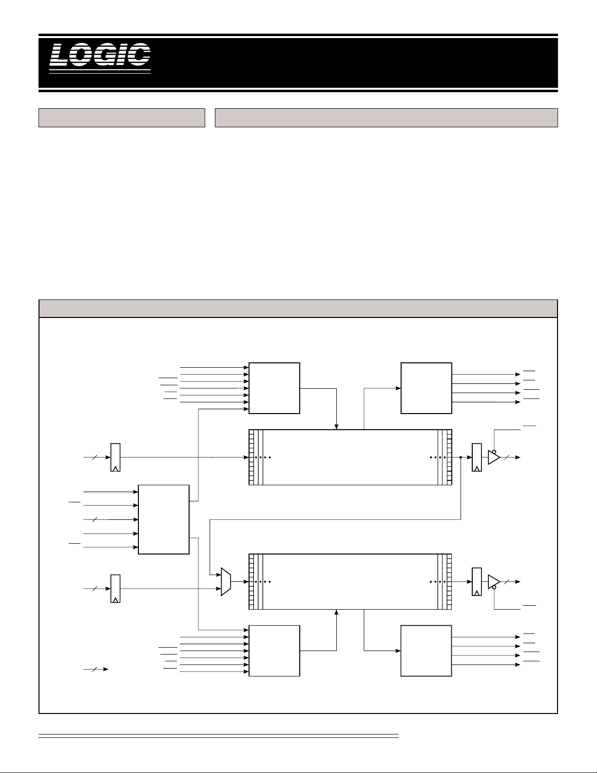
The LF3304 is a dual line buffer/
FIFO, designed to operate at HDTV
rates. The LF3304 will operate in
two distinct modes: Line Buffer and
FIFO. In these modes the two memories can operate independently or
with common control.
The LF3304 comprises two 12-bit 4K
memories configurable in a variety of
ways including: Two 12-bit 4K deep
line buffers (independent lengths),
Three 8-bit 4K deep line buffers
LF3304 BLOCK DIAGRAM
Dual Line Buffer/FIFO
(common lengths), One 12-bit 8K
deep line buffer, or Two 12-bit 4K
FIFOs (independent operation).
In FIFO mode, independent Read
and Write Resets give the designer
control over the internal pointers
providing flexibility not commonly
found in ordinary FIFOs.
The LF3304 operatates at a maximum
data rate of 100 MHz and is available
in a 100-lead PQFP package.
AIN11-0
ADDRA
LENGTH
ADDRB
BIN11-0
MODE1-0
LDA
11-0
LDB
WCLKA
RCLKA
WENA
RENA
RRA
RWA
12
12
12
2
MASTER
CONTROL
WCLKB
RCLKB
WENB
RENB
RRB
RWB
RAM ARRAY 1
CONTROL
VARIABLE LENGTH RAM ARRAY A
4K x 12-bit
VARIABLE LENGTH RAM ARRAY B
4K x 12-bit
RAM ARRAY 2
CONTROL
FLAG
GENERATOR
FLAG
GENERATOR
12
12
FFA
EFA
PAFA
PAEA
OEA
AOUT11-0
BOUT11-0
OEB
FFB
EFB
PAFB
PAEB
Video Imaging Products
1
08/16/2000–LDS.3304-F
DEVICES INCORPORATED
LF3304
Dual Line Buffer/FIFO
LINE BUFFER MODE
SIGNAL DEFINITIONS
Power
VCC and GND
+3.3 V power supply. All pins must
be connected.
Clocks
WCLKA — Write Clock A
WCLKA and RCLKA must be tied
together for RAM Array A to properly
operate as a Line Buffer. The rising edge
of xCLKA strobes all appropriate
enabled registers.
RCLKA — Read Clock A
See WCLKA description.
WCLKB — Write Clock B
WCLKB and RCLKB must be tied
together for RAM Array B to properly
operate as a Line Buffer. The rising
edge of xCLKB strobes all appropriate
enabled registers.
RCLKB — Read Clock B
See WCLKB description.
Inputs
AIN11-0 — Data Input A
AIN11-0 is the 12-bit registered data
input port.
BIN11-0 — Data Input B
BIN11-0 is the 12-bit registered data
input port.
LENGTH11-0 — Line Buffer Length
The 12-bit value is used to specify the
length of each of the RAM Arrays. An
integer value ranging from 0 to 4095 is
used to select a delay ranging from 2 to
4097 clock cycles. The value placed on
LENGTH11-0 is equal to the desired delay
minus 8. To set the length of RAM Array A
the data presented on LENGTH11-0 is
loaded into the device on the active edge of
WCLKA in conjunction with LDA being
driven LOW. To set the length of RAM
Array B the data presented on
LENGTH11-0 is loaded into the device
on the active edge of WCLKB in
conjunction with LDB being driven
LOW. If an equal length is desired for
both RAM Arrays, the data presented
on LENGTH11-0 is loaded into the
device on the active edge of WCLK
(WCLKA and WCLKB tied together) in
conjuction with LDx (LDA and LDB
tied together) being driven LOW.
MODE1-0 — Mode Select
The mode select inputs determine the
operating mode of the LF3304 (Table 1) for
data being input on the next clock cycle.
When switching between modes, the
internal pipeline latencies of the device
must be observed. After switching
operating modes, either the user must
allow enough clock clycles to pass to flush
the internal RAM Array or RWx and RRx
must be driven LOW together before valid
data will appear on the outputs.
Controls
LDA — RAM Array A Load
When LDA is LOW, data on
LENGTH11-0 is latched in the length
register on the rising edge of xCLKA.
LDB — RAM Array B Load
When LDB is LOW, data on
LENGTH11-0 is latched in the length
register on the rising edge of xCLKB.
WENA — Write Enable A
Driving WENA LOW places the device in
programmable delay mode and driving
WENA HIGH places RAM Array A in
recirculate mode (programmable circular
buffer). When in recirculate mode, the
write pointer position remains fixed while
data on AIN11-0 is ignored. When
switching back from recirculate mode to
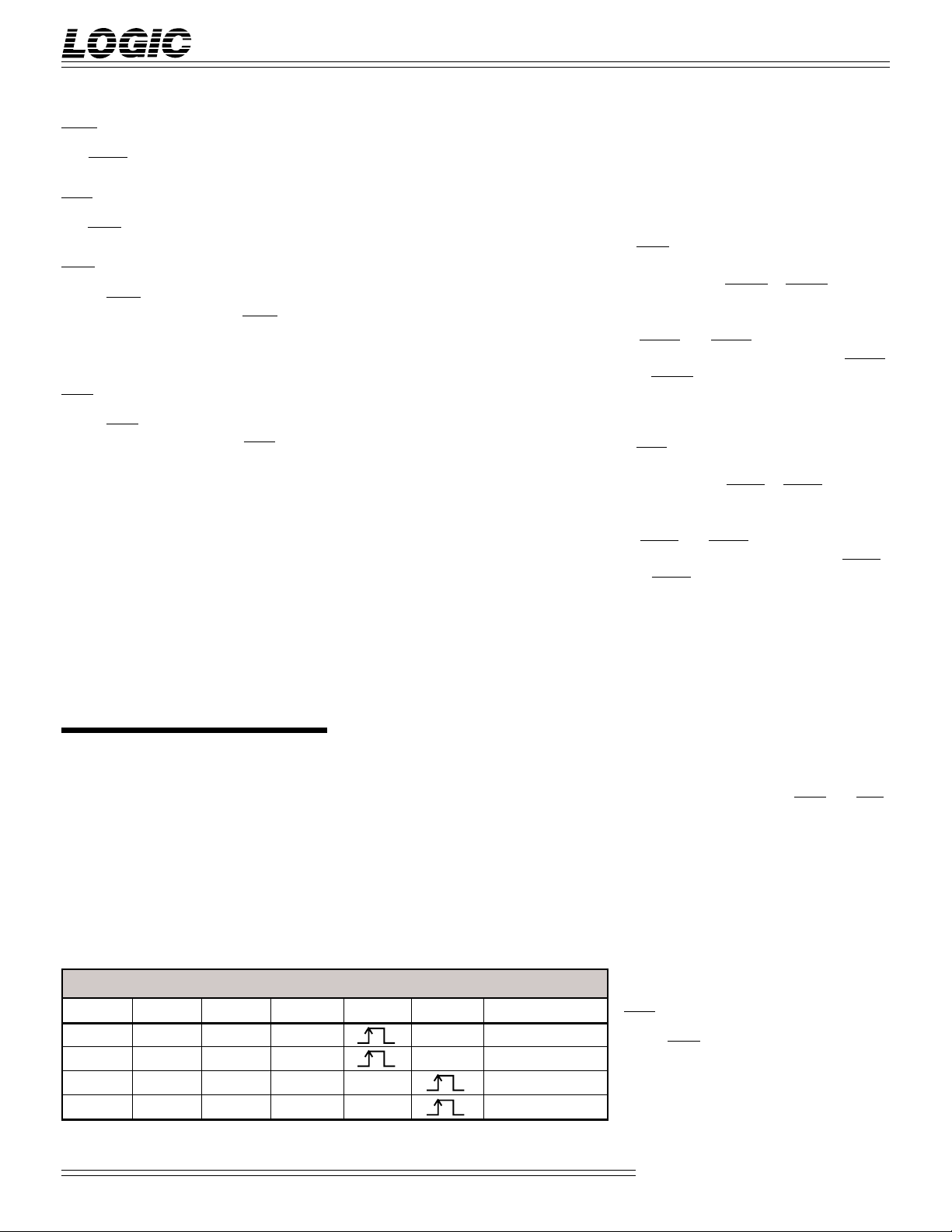
TABLE 1. DEVICE CONFIGURATION
MODE1-0 Mode Select
0 0 Dual Line Buffer
0 1 Cascaded Line Buffer
1 0 Dual FIFO
1 1 Reserved
delay mode, RWA and RRA should be
brought LOW to properly reset the Write
and Read pointers.
RENA — Read Enable B
In Line Buffer mode, RENA must be
kept LOW.
WENB — Write Enable B
Driving WENB LOW places the device in
programmable delay mode and driving
WENB HIGH places RAM Array B in
recirculate mode (programmable circular
buffer). When in recirculate mode, the
write pointer position remains fixed
while data on BIN11-0 is ignored. When
switching back from recirculate mode to
delay mode, RWB and RRB should be
brought LOW to properly reset the Write
and Read pointers.
RENB — Read Enable B
In Line Buffer mode, RENB must be
kept LOW.
RWA — Reset Write A
The write address pointer is reset to the
first physical location when RWA is set
LOW. After power up, the LF3304
requires a Reset Write for initialization
because the write address pointer is not
defined at that time.
RRA — Reset Read A
The read address pointer is reset to the
first physical location when RRA is set
LOW. After power up, the LF3304
requires a Reset Read for initialization
because the read address pointer is not
defined at that time.
Video Imaging Products
8
2
08/16/2000–LDS.3304-F
DEVICES INCORPORATED
LF3304
Dual Line Buffer/FIFO
RWB — Reset Write B
See RWA Description.
RRB — Reset Read B
See RRA description.
OEA — Output Enable A
When OEA is LOW, AOUT11-0 is
enabled for output. When OEA is
HIGH, AOUT11-0 is placed in a highimpedence state.
OEB — Output Enable B
When OEB is LOW, BOUT11-0 is
enabled for output. When OEB is
HIGH, BOUT11-0 is placed in a highimpedence state.
Outputs
AOUT11-0 — Data Output A
AOUT11-0 is the 12-bit registered
data output port.
BOUT11-0 — Data Output B
BOUT11-0 is the 12-bit registered
data output port.
FIFO MODE
SIGNAL DEFINITIONS
Power
VCC and GND
+3.3 V power supply. All pins must be
connected.
Clocks
WCLKA — Write Clock A
Data present on AIN11-0 is written
into the LF3304 on the rising edge of
WCLKA when the device is configured
for writing.
RCLKA — Read Clock A
Data is read from the LF3304 and
presented on the output port (AOUT11-0)
after tD has elapsed from the rising
edge of RCLKA when the device is
configured for reading and the output
port is enabled. WCLKA and RCLKA
can be tied together and driven by the
same external clock or they may be
controlled by separate external clocks.
WCLKB — Write Clock B
Data present on BIN11-0 is written into
the LF3304 on the rising edge of
WCLKB when the device is configured
for writing.
RCLKB — Read Clock B
Data is read from the LF3304 and
presented on the output port (BOUT11-0)
after tD has elapsed from the rising
edge of RCLKB when the device is
configured for reading and the output
port is enabled. WCLKB and RCLKB
can be tied together and driven by the
same external clock or they may be
controlled by separate external clocks.
Inputs
AIN11-0 — Data Input A
AIN11-0 is the 12-bit registered data
input port.
BIN11-0 — Data Input B
BIN11-0 is the 12-bit registered data
input port.
ADDRA — Address A
If LDA is LOW, on the rising edge of
WCLKA data present on AIN11-0 is
written into the PAFA or PAEA register
depending on ADDRA (see Table 2).
The LSB, AIN0, corresponds to the LSB
of PAFA and PAEA registers. The MSB,
AIN11, corresponds to the MSB of PAFA
and PAEA registers.
ADDRB — Address B
If LDB is LOW, on the rising edge of
WCLKB data present on BIN11-0 is
written into the PAFB or PAEB register
depending on ADDRB (see Table 2).
The LSB, BIN0, corresponds to the LSB
of PAFB and PAEB registers. The MSB,
BIN11, corresponds to the MSB of PAFB
and PAEB registers.
MODE1-0 — Mode Select
The mode select inputs determine the
operating mode of the LF3304 (Table 1) for
data being input on the next clock cycle.
When switching between modes, the
internal pipeline latencies of the device
must be observed. After switching
operating modes, either the user must
allow enough clock clycles to pass to flush
the internal RAM Array or RWx and RRx
must be driven LOW together before valid
data will appear on the outputs.
LENGTH — Non-Flag Pins
In FIFO Mode, the unused LENGTH pins
(LENGTH11, LENGTH10, LENGTH5,
LENGTH4) must be tied LOW.
TABLE 2. LOADING PROGRAMMABLE FLAG REGISTERS
ADDRA ADDRB LDA LDB WCLKA WCLKB Operation
0 x 0 x x PAEA Register
1 x 0 x x PAFA Register
x 0 x 0 x PAEB Register
x 1 x 0 x PAFB Register
3
Controls
LDA — RAM Array A Load
When LDA is LOW, data on AIN11-0 is
latched in the LF3304 on the rising edge
of WCLKA.
Video Imaging Products
08/16/2000–LDS.3304-F

DEVICES INCORPORATED
LF3304
Dual Line Buffer/FIFO
LDB — RAM Array B Load
When LDB is LOW, data on BIN11-0 is
latched in the LF3304 on the rising
edge of WCLKB.
WENA — Write Enable A
If WENA is LOW, data on AIN11-0 is
written to the device on the rising edge
of WCLKA. When RAM Array A is
full, WENA is ignored.
RENA — Read Enable A
If RENA is LOW, data from RAM Array
A is read and presented on AOUT11-0
after tD has elapsed from the rising
edge of RCLKA if the output port is
enabled. If RENA goes HIGH, the last
value loaded in the RAM Array A
output register will remain unchanged.
When RAM Array A is empty, RENA is
ignored.
WENB — Write Enable B
If WENB is LOW, data on BIN11-0 is
written to the device on the rising edgle
of WCLKB. When RAM Array B is full,
WENB is ignored.
RENB — Read Enable B
If RENB is LOW, data from RAM Array
B is read and presented on BOUT11-0
after tD has elapsed from the rising
edge of RCLKB if the output port is
enabled. If RENB goes HIGH, the last
value loaded in the RAM Array B
output register will remain unchanged.
When RAM Array B is empty, RENB is
ignored.
RWA — Reset Write A
The write address pointer is reset to the
first physical location when RWA is set
LOW. After power up, the LF3304
requires a Reset Write for initialization
because the write address pointer is not
defined at that time.
RRA — Reset Read A
The read address pointer is reset to the first
physical location when RRA is set LOW.
After power up, the LF3304 requires a Reset
Read for initialization because the read
address pointer is not defined at that time.
RWB — Reset Write B
See RWA Description.
RRB — Reset Read B
See RRA description.
OEA — Output Enable A
When OEA is LOW, AOUT11-0 is
enabled for output. When OEA is
HIGH, AOUT11-0 is placed in a highimpedence state. The flag outputs are
not affected by OEA.
OEB — Output Enable B
When OEB is LOW, BOUT11-0 is
enabled for output. When OEB is
HIGH, BOUT11-0 is placed in a highimpedence state. The flag outputs are
not affected by OEB.
Outputs
AOUT11-0 — Data Output A
AOUT11-0 is the 12-bit registered data
output port.
BOUT11-0 — Data Output B
BOUT11-0 is the 12-bit registered data
output port.
FFA — Full Flag A
FFA goes LOW when RAM Array A is
full of data. When FFA is LOW, RAM
Array A can not be written to. The Full
Flag is synchronized to the rising edge
of WCLKA.
EFA — Empty Flag A
EFA goes LOW when the read pointer is
equal to the write pointer, indicating that
RAM Array A is empty. When EFA is
LOW, read operations can not be
performed. The Empty Flag is synchronized to the rising edge of RCLKA.
FFB — Full Flag B
FFB goes LOW when RAM Array B is full
of data. When FFB is LOW, RAM Array B
can not be written to. The Full Flag is
synchronized to the rising edge of WCLKB.
EFB — Empty Flag B
EFB goes LOW when the read pointer
is equal to the write pointer, indicating
that RAM Array B is empty. When EFB
is LOW, read operations can not be
performed. The Empty Flag is synchronized to the rising edge of RCLKB.
PAFA — Programmable Almost-Full Flag A
PAFA goes LOW when the write
pointer is (Full – N) locations ahead of
the read pointer. N is the value stored
in the PAFA register and has no default
value. PAFA is synchronized to the
rising edge of WCLKA.
PAEA — Programmable Almost-Empty Flag A
PAEA goes HIGH when the write
pointer is (N + 1) location ahead of the
read pointer. N is the value stored in
the PAEA register and has no default
value. PAEA is synchronized to the
rising edge of RCLKA.
PAFB — Programmable Almost-Full Flag B
PAFB goes LOW when the write pointer
is (Full – N) locations ahead of the read
pointer. N is the value stored in the
PAFB register and has no default value.
PAFB is synchronized to the rising
edge of WCLKB.
PAEB — Programmable Almost-Empty Flag B
PAEB goes HIGH when the write
pointer is (N + 1) location ahead of the
read pointer. N is the value stored in
the PAEB register and has no default
value. PAEB is synchronized to the
rising edge of RCLKB.
Video Imaging Products
4
08/16/2000–LDS.3304-F

DEVICES INCORPORATED
LF3304
Dual Line Buffer/FIFO
FIFO MODE
OPERATION
Initialization
Upon power-up, the LF3304 requires
the initialization of the internal read
and write address pointers. This
initialization sequence can be done
by either a Flag Enable Reset or a
Flag Disable Reset.
A Flag Enable Reset will force the
FIFO to operate in a ‘Flag Enabled’
mode. In this mode, writing will be
disabled when FFx is LOW and
reading is disabled when EFx is
LOW. Any ‘write beyond full’ event
or ‘read beyond empty’ event will be
disabled. Note: in an ‘empty’ state,
the last data word read from the
FIFO is held on the output bus until
the next valid read cycle.
A Flag Disable Reset will force the
FIFO to operate in a ‘Flag Disabled’
mode. In this mode, the user is
allowed to write over previously unread data and read out previously
read data. Consequently, any
enabled write or read is valid thus
allowing the write and read pointers
to ‘wrap-around’. Note: due to the
nature of this mode, the flag status
should be disregarded. For example,
as the 4096th data word is written
into the FIFO, assuming that no
preceding read cycles have occured,
FFx will be driven LOW thus indicating a ‘full’state. While the FIFO is
still in this ‘full’ state, the next
enabled write will access address
000H, thus writing over data that
has not yet been read out.
Flag Enable Reset
A Flag Enable Reset resets the read
and write pointers and enables the
flags to control the reading and
writing of data according to the Full
Flag and Empty Flag conditions. A
Flag Enable Reset occurs when the
following conditions are met:
1. RWA/RWB must be LOW for at
least one WCLKA/WCLKB cycle.
2. RRA/RRB must be LOW for at
least one RCLKA/RCLKB cycle.
3. WENx and RENx must be HIGH
during the above two conditions
plus one addition write or read
cycle (which ever is longer).
The Flag Enable Reset condition can
be disabled if one of the two Flag
Disable Reset conditions are applied.
Flag Disable Reset
A Flag Disable Reset resets the read
and write pointers and disables the
flags from controlling the reading
and writing of data. A Flag Disable
Reset occurs when the following
conditions are met:
1. RWA/RWB must be LOW for at
least one WCLKA/WCLKB cycle
while WENx is LOW.
2. RRA/RRB must be LOW for at
least one RCLKA/RCLKB cycle
while RENx is LOW.
Configuration of Programmable Flags
In order to load a FIFO A Programmable Flag Register, a rising edge of
WCLKA, while WENA is LOW,
latches AIN11-0 into either the PAFA
or PAEA Register - depending on the
states of ADDRA and LDA (See
Table 2).
In order to load a FIFO B Programmable Flag Register, a rising edge of
WCLKB, while WENB is LOW,
latches BIN11-0 into either the PAFB
or PAEB Register - depending on the
states of ADDRB and LDB (See Table
2). See the Figure labeled “Program-
mable Flag Load Timing.”
Video Imaging Products
5
08/16/2000–LDS.3304-F

DEVICES INCORPORATED
LF3304
Dual Line Buffer/FIFO
MAXIMUM RATINGS
Storage temperature ............................................................................................................. –65°C to +150°C
Operating ambient temperature............................................................................................. –55°C to +125°C
VCC supply voltage with respect to ground ............................................................................ –0.5 V to +4.5V
Input signal with respect to ground........................................................................................... –0.5 V to 5.5 V
Signal applied to high impedance output .................................................................................. –0.5 V to 5.5 V
Output current into low outputs ............................................................................................................. 25 mA
Latchup current................................................................................................................................ > 400 mA
OPERATING CONDITIONS
Active Operation, Commercial 0°C to +70°C 3.00 V ≤ VCC ≤ 3.60 V
Active Operation, Military –55°C to +125°C 3.00 V ≤ VCC ≤ 3.60 V
Above which useful life may be impaired (Notes 1, 2, 3, 8)
To meet specified electrical and switching characteristics
Mode Temperature Range (Ambient) Supply Voltage
ELECTRICAL CHARACTERISTICS
Symbol Parameter Test Condition Min Typ M ax Unit
VOH Output High Voltage VCC = Min., IOH = –4 mA 2.4 V
VOL Output Low Voltage VCC = Min., IOL = 8.0 mA 0.4 V
VIH Input High Voltage 2.0 5.5 V
V IL Input Low Voltage (Note 3) 0.0 0.8 V
IIX Input Current Ground ≤ VIN ≤ VCC (Note 12) ±10 µA
IOZ Output Leakage Current Ground ≤ VOUT ≤ VCC (Note 12) ±10 µA
ICC1 VCC Current, Dynamic (Notes 5, 6) 50 mA
ICC2 VCC Current, Quiescent (Note 7) 2mA
CIN Input Capacitance TA = 25°C, f = 1 MHz 1 0 pF
COUT Output Capacitance TA = 25°C, f = 1 MHz 1 0 pF
Over Operating Conditions (Note 4)
Video Imaging Products
6
08/16/2000–LDS.3304-F

DEVICES INCORPORATED
SWITCHING CHARACTERISTICS
LF3304
Dual Line Buffer/FIFO
COMMERCIAL OPERATING RANGE (0°C to +70°C)
Symbol Parameter Min Max Min Max Min Max
tCYC Cycle Time 1 5 1 2 1 0
tPWH Clock Pulse Width High 5 4 3
tPWL Clock Pulse Width Low 5 4 3
tDS Data Setup Time 6 5 4
tDH Data Hold Time 0 0 0
tWES Write Enable Setup Time 6 5 4
tWEH Write Enable Hold Time 0 0 0
tRES Read Enable Setup Time 6 5 4
tREH Read Enable Hold Time 0 0 0
tLDS Load Setup Time 6 5 4
tLDH Load Hold Time 0 0 0
tRS Read/Write Reset Setup Time 6 5 4
tRH Read/Write Reset Hold Time 0 0 0
tAC Access Time 8 7 6
Notes 9, 10 (ns)
LF3304–
15 12 10
tWFF Write Clock to Full Flag 8 7 6
tREF Read Clock to Empty Flag 8 7 6
tPAF Write Clock to Programmable Almost-Full Flag 8 7 6
tPAE Read Clock to Programmable Almost-Empty Flag 8 7 6
tOHZ Output Enable to Output in Low Impedance 8 7 6
tOLZ Output Enable to Output in High Impedance 8 7 6
tSKEW1 Skew Time Between Read and Write Clocks for EF and FF 6 5 4
tSKEW2 Skew Time Between Read and Write Clocks for PAEx and PAFx 6 5 4
Video Imaging Products
7
08/16/2000–LDS.3304-F

DEVICES INCORPORATED
WRITE CYCLE TIMING
WCLKA
WCLKB
t
PWHtPWL
WENA
WENB
AIN
11–0
BIN
11–0
FF
RCLKA
RCLKB
RWA = RWB = HIGH
t
CYC
tDSt
(n) (n+1)
DH
t
SKEW1
t
WES
t
WEH
(n+2)
LF3304
Dual Line Buffer/FIFO
(n+3)
t
WFF
t
WFF
READ CYCLE TIMING
RCLKA
RCLKB
t
PWHtPWL
t
RENA
RENB
AOUT
11–0
BOUT
11–0
EF
WCLKA
WCLKB
RRA = RRB = HIGH
OEA = OEB = LOW
(n–2) (n–1) (n) (n+1) (n+2) (n+3)
CYC
t
AC
t
SKEW1
t
REF
t
RES
t
REF
t
REH
Video Imaging Products
8
08/16/2000–LDS.3304-F

DEVICES INCORPORATED
WRITE RESET TIMING
WCLKA
WCLKB
RWA
RWB
AIN
11–0
BIN
(n-1) (n) (n+1)
11–0
WENA = WENB = LOW
READ RESET TIMING
RCLKA
RCLKB
RRA
RRB
AOUT
11–0
BOUT
(n–2) (n–1) (n)
11–0
LF3304
Dual Line Buffer/FIFO
t
RS
tDSt
DH
t
RS
t
AC
(n+1)
t
RH
(n+2) (0) (0) (1)
t
RH
(0)(n+2) (1)
RENA = RENB = LOW
OEA = OEB = LOW
PROGRAMMABLE FLAG LOAD TIMING
WCLKA
WCLKB
AIN
BIN
ADDRA
ADDRB
WENA
WENB
11–0
11–0
LDA
LDB
tDSt
DH
PAEx PAFx
t
LDS
t
LDH
Video Imaging Products
9
08/16/2000–LDS.3304-F

DEVICES INCORPORATED
PROGRAMMABLE ALMOST FULL FLAG
WCLKA
WCLKB
PAFA
PAFB
RCLKA
RCLKB
PROGRAMMABLE ALMOST EMPTY FLAG
WCLKA
WCLKB
PAEA
PAEB
t
PAE
RCLKA
RCLKB
tPAF
t
SKEW2
tSKEW2
t
PAE
LF3304
Dual Line Buffer/FIFO
tPAF
OUTPUT ENABLE AND DISABLE
OEA
OEB
AOUT
11–0
BOUT
11–0
t
OHZ
HIGH IMPEDANCE
t
OLZ
Video Imaging Products
10
08/16/2000–LDS.3304-F

DEVICES INCORPORATED
OE
0.2 V
t
DIS
t
ENA
0.2 V
1.5 V 1.5 V
3.0V Vth
1
Z
0
Z
Z
1
Z
0
1.5 V
1.5 V
0V Vth
VOL*
V
OH
*
V
OL
*
V
OH
*
Measured V
OL
with IOH = –10mA and IOL = 10mA
Measured V
OH
with IOH = –10mA and IOL = 10mA
NOTES
LF3304
Dual Line Buffer/FIFO
1. Maximum Ratings indicate stress
specifications only. Functional operation of these products at values beyond
those indicated in the Operating Conditions table is not implied. Exposure to
maximum rating conditions for extended periods may affect reliability.
2. The products described by this specification include internal circuitry designed to protect the chip from damaging
substrate injection currents and accumulations of static charge. Nevertheless, conventional precautions should
be observed during storage, handling,
and use of these circuits in order to avoid
exposure to excessive electrical stress
values.
3. This device provides hard clamping
of transient undershoot. Input levels
below ground will be clamped beginning at –0.6 V. The device can withstand
indefinite operation with inputs or outputs in the range of –0.5 V to +5.5 V.
Device operation will not be adversely
affected, however, input current levels
will be well in excess of 100 mA.
input transition times less than 3 ns,
output reference levels of 1.5 V (except
tDIS test), and input levels of nominally
0 to 3.0 V. Output loading may be a
resistive divider which provides for
specified IOH and IOL at an output
voltage of VOH min and VOL max
respectively. Alternatively, a diode
bridge with upper and lower current
sources of IOH and IOL respectively,
and a balancing voltage of 1.5 V may be
used. Parasitic capacitance is 30 pF
minimum, and may be distributed.
This device has high-speed outputs capable of large instantaneous current
pulses and fast turn-on/turn-off times.
As a result, care must be exercised in the
testing of this device. The following
measures are recom mended:
a. A 0.1 µF ceramic capacitor should be
installed between VCC and Ground
leads as close to the Device Under Test
(DUT) as possible. Similar capacitors
should be installed between device VCC
and the tester common, and device
ground and tester common.
measured to the 1.5 V crossing point with
datasheet loads. For the tDIS test, the
transition is measured to the ±200mV
level from the measured steady-state
output voltage with ±10mA loads.
The balancing voltage, VTH, is set at
3.0 V for Z-to-0 and 0-to-Z tests, and
set at 0 V for Z-to-1 and 1-to-Z tests.
12. These parameters are only tested at
the high temperature extreme, which is
the worst case for leakage current.
FIGURE A. OUTPUT LOADING CIRCUIT
DUT
S1
I
OL
V
C
L
I
TH
OH
FIGURE B. THRESHOLD LEVELS
4. Actual test conditions may vary from
those designated but operation is guaranteed as specified.
5. Supply current for a given application can be accurately approximated
by:
2
NCV F
where
4
N = total number of device outputs
C = capacitive load per output
V = supply voltage
F = clock frequency
b. Ground and VCC supply planes must
be brought directly to the DUT socket or
contactor fingers.
c. Input voltages on a test fixture should
be adjusted to compensate for inductive
ground and VCC noise to maintain required DUT input levels relative to the
DUT ground pin.
10. Each parameter is shown as a minimum or maximum value. Input requirements are specified from the point of view
of the external system driving the chip.
Setup time, for example, is specified as a
minimum since the external system must
6. Tested with outputs changing every
cycle and no load, at a 40 MHz clock rate.
supply at least that much time to meet the
worst-case requirements of all parts.
Responses from the internal circuitry are
7. Tested with all inputs within 0.1 V of
VCC or Ground, no load.
8. These parameters are guaranteed but
not 100% tested.
9. AC specifications are tested with
specified from the point of view of the
device. Output delay, for example, is
specified as a maximum since worstcase operation of any device always provides data within that time.
11. For the tENA test, the transition is
11
Video Imaging Products
08/16/2000–LDS.3304-F

DEVICES INCORPORATED
ORDERING INFORMATION
100-pin
GND
VCC
AIN
AIN
AIN
AIN
AIN
AIN
AIN
AIN
AIN
AIN
AIN
AIN
GND
VCC
BIN
BIN
BIN
BIN
BIN
BIN
BIN
BIN
BIN
BIN
BIN
BIN
GND
VCC
LF3304
Dual Line Buffer/FIFO
0
1
2
3
WENA
RWA
WCLKA
RCLKA
RRA
RENA
VCC
GND
MODE0LDA
ADDRA
OEA
VCC
GND
LENGTH5LENGTH4FFA/LENGTH
EFA/LENGTH
PAFA/LENGTH
PAEA/LENGTH
99989796959493929190898887868584838281
100
1
2
0
3
1
4
2
5
3
6
4
7
5
8
6
9
7
10
8
11
12
9
10
13
14
11
15
16
0
17
18
1
19
2
20
3
21
4
22
5
23
6
24
7
25
8
26
9
27
10
28
11
29
30
31323334353637383940414243444546474849
Top
View
VCC
80
GND
79
AOUT
78
77
76
75
74
73
72
71
70
69
68
67
66
65
64
63
62
61
60
59
58
57
56
55
54
53
52
51
50
AOUT
AOUT
AOUT
AOUT
AOUT
AOUT
AOUT
AOUT
AOUT
AOUT
AOUT
VCC
GND
BOUT
BOUT
BOUT
BOUT
BOUT
BOUT
BOUT
BOUT
BOUT
BOUT
BOUT
BOUT
VCC
GND
0
1
2
3
4
5
6
7
8
9
10
11
0
1
2
3
4
5
6
7
8
9
10
11
Speed
15 ns
12 ns
10 ns
0°C to +70°C — COMMERCIAL SCREENING
1
RWB
WENB
RCLKB
WCLKB
RRB
GND
RENB
VCC
LDB
MODE
Plastic Quad Flatpack
(Q2)
LF3304QC15
LF3304QC12
LF3304QC10
OEB
ADDRB
GND
11
VCC
LENGTH
10
/FFB
/EFB
9
8
LENGTH
LENGTH
LENGTH
/PAFB
/PAEB
7
6
LENGTH
LENGTH
Video Imaging Products
12
08/16/2000–LDS.3304-F
 Loading...