

LITTELFUSE V9MLA0805LWT, V9MLA0805LWA, V9MLA0805LWH, V9MLA0805LT, V9MLA0805LH Datasheet
...
Multilayer Transient Voltage Surge Suppressors
ML Varistor Series
Surface Mount Varistors
140
www.littelfuse.com
The ML Series family of Transient Voltage Surge Suppression devices is
based on the Littelfuse Multilayer fabrication technology. These components are designed to suppress a variety of transient events, including
those specified in IEC 61000-4-2 or other standards used for Electromagnetic
Compliance (EMC). The ML Series is typically applied to protect integrated
circuits and other components at the circuit board level.
The wide operating voltage and energy range make the ML Series suitable for numerous applications on power supply, control and signal lines.
The ML Series is manufactured from semiconducting ceramics, and is
supplied in a leadless, surface mount package.The ML Series is compatible with modern reflow and wave soldering procedures.
It can operate over a wider temperature range than zener diodes, and
has a much smaller footprint than plastic-housed components.
Littelfuse Inc. manufactures other Multilayer Series products. See the
MLE Series data sheet for ESD applications, MHS Series data sheet for
high-speed ESD applications, the MLN for multiline protection and the
AUML Series for automotive applications.
Features
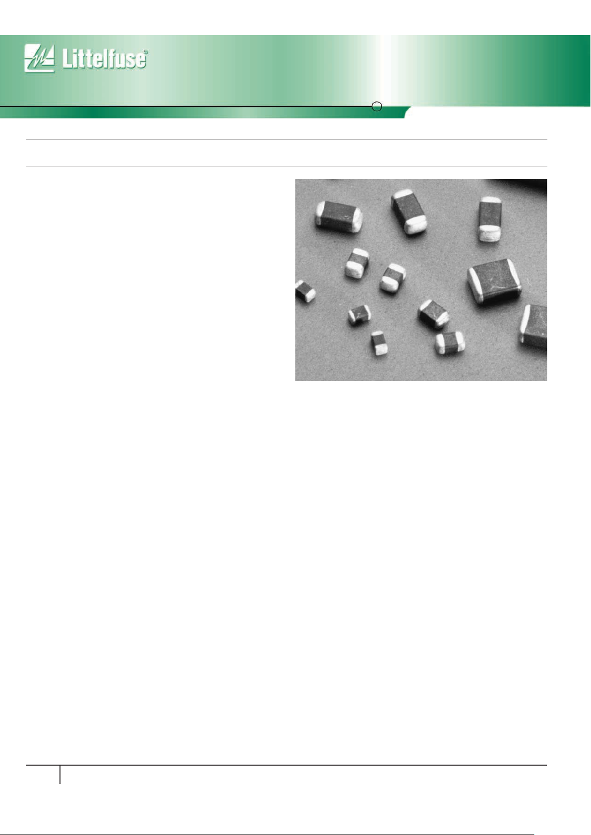
• Leadless 0402, 0603, 0805, 1206 and 1210 Chip Sizes
• Multilayer Ceramic Construction Technology
•-55oC to +125oC Operating Temperature Range
• Operating Voltage Range V
M(DC)
= 5.5V to 120V
• Rated for Surge Current (8 x 20µs)
• Rated for Energy (10 x 1000µs)
• Inherent Bi-directional Clamping
• No Plastic or Epoxy Packaging Assures Better than 94V-0
Flammability Rating
• Standard Low Capacitance Types Available
Applications
• Suppression of Inductive Switching or Other Transient Events Such
as EFT and Surge Voltage at the Circuit Board Level
• ESD Protection for Components Sensitive to IEC 61000-4-2,
MIL-STD-883C Method 3015.7, and Other Industry Specifications
(See Also the MLE or MLN Series)
• Provides On-Board Transient Voltage Protection for ICs and Transistors
• Used to Help Achieve Electromagnetic Compliance of End Products
• Replace Larger Surface Mount TVS Zeners in
Many Applications
Absolute Maximum Ratings For ratings of individual members of a series, see Device Ratings and Specifications table.
Continuous:
Steady State Applied Voltage:
DC Voltage Range (V
M(DC)
). . . . . . . . . . . . . . . . . . . . . . . . . . . . . . . . . . . . . . . . . . . . . . . . . . . . . . . . . . . . . . . . . . . . . . . . . 3.5 to 120 V
AC Voltage Range (V
M(AC)RMS
) . . . . . . . . . . . . . . . . . . . . . . . . . . . . . . . . . . . . . . . . . . . . . . . . . . . . . . . . . . . . . . . . . . . . . 2.5 to 107 V
Transient:
Non-Repetitive Surge Current, 8/20µs Waveform, (ITM) . . . . . . . . . . . . . . . . . . . . . . . . . . . . . . . . . . . . . . . . . . . . . . . . . . . . . 4 to 500 A
Non-Repetitive Surge Energy, 10/1000µs Waveform, (WTM) . . . . . . . . . . . . . . . . . . . . . . . . . . . . . . . . . . . . . . . . . . . . . . . . . 0.2 to 2.5 J
Operating Ambient Temperature Range (TA) . . . . . . . . . . . . . . . . . . . . . . . . . . . . . . . . . . . . . . . . . . . . . . . . . . . . . . . . . . . . . . -55 to + 125
O
C
Storage Temperature Range (T
STG
) . . . . . . . . . . . . . . . . . . . . . . . . . . . . . . . . . . . . . . . . . . . . . . . . . . . . . . . . . . . . . . . . . . . . -55 to + 150
O
C
Temperature Coefficient (αV) of Clamping Voltage (VC) at Specified Test Current . . . . . . . . . . . . . . . . . . . . . . . . . . . . . . . . . . . . . <0.01 %/OC
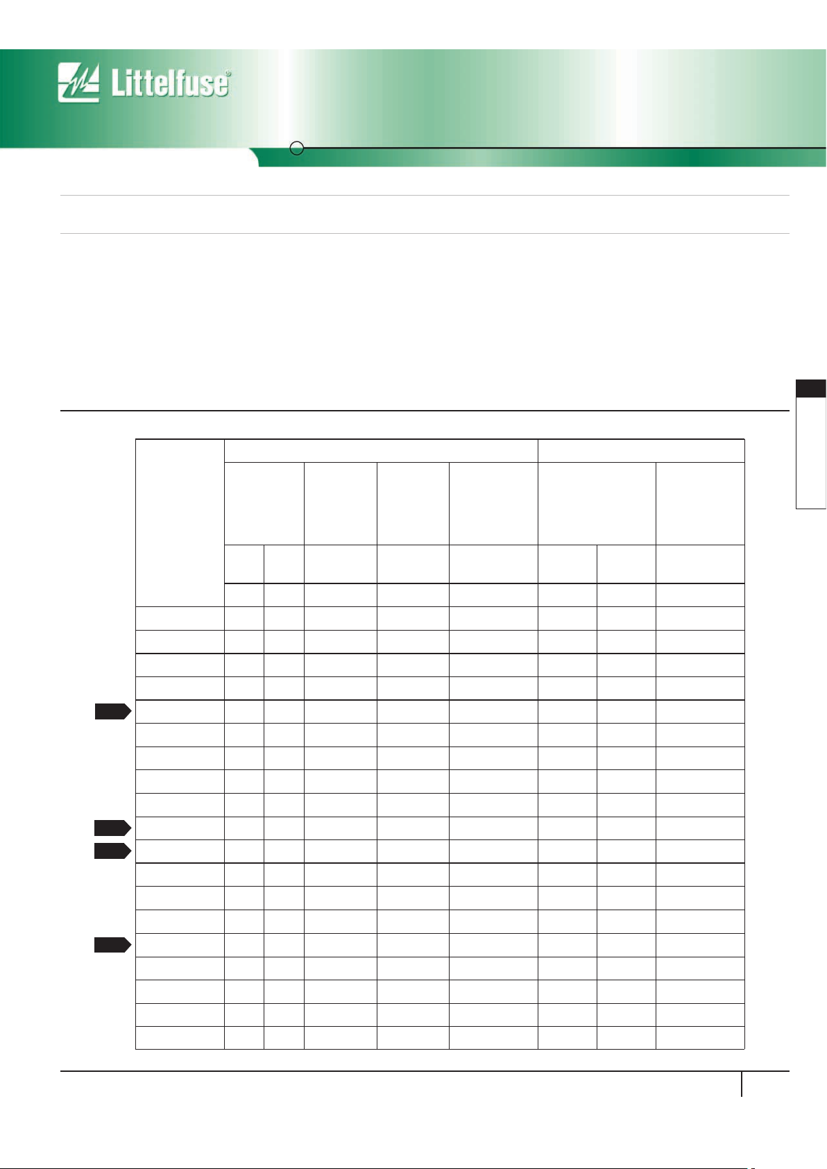
Device Ratings and Specifications
ML SERIES UNITS
PA RT
NUMBER
MAXIMUM RATINGS (125
o
C) SPECIFICATIONS (25oC)
MAXIMUM
CONTINUOUS
WORKING
VO LTAGE
MAXIMUM
NON-
REPETITIVE
SURGE
CURRENT
(8/20µs)
MAXIMUM
NON-
REPETITIVE
SURGE
ENERGY
(10/1000µs)
MAXIMUM
CLAMPING
VO LTAG E AT
10A
(OR AS NOTED)
(8/20µs)
NOMINAL VOLTAGE
AT 1mA DC TEST
CURRENT
TYPICAL
CAPACITANCE
AT f = 1MHz
V
M(DC)VM(AC)
I
TM
W
TM
V
C
V
N(DC)
MIN
V
N(DC)
MAX C
(V) (V) (A) (J) (V) (V) (V) (pF)
V3.5MLA0603 3.5 2.5 30 0.1 10 at 2A 3.7 7.0 1100
V3.5MLA0805 3.5 2.5 120 0.3 10 at 5A 3.7 7.0 2200
V3.5MLA0805L 3.5 2.5 40 0.1 10 at 2A 3.7 7.0 1200
V3.5MLA1206 3.5 2.5 100 0.3 14 3.7 7.0 6000
V5.5MLA0402 5.5 4.0 20 0.050 15.5 at 1A 7.1 9.3 220
V9MLA0402 9 6.5 20 0.050 22 at 1A 11 14 120
V9MLA0402L 9 6.5 4 0.020 25 at 1A 11 14 33
V14MLA0402 14 10 20 0.050 30 at 1A 15.9 20.3 70
V5.5MLA0603 5.5 4.0 30 0.1 15.5 at 2A 7.1 9.3 660
V5.5MLA0805 5.5 4.0 120 0.3 15.5 at 5A 7.1 9.3 1600
V5.5MLA0805L 5.5 4.0 40 0.1 15.5 at 2A 7.1 9.3 860
V5.5MLA1206 5.5 4.0 150 0.4 15.5 7.1 9.3 4500
V9MLA0603 9.0 6.5 30 0.1 23 at 2A 11.0 16.0 420
V9MLA0805L 9.0 6.5 40 0.1 20 at 2A 11 14 450
V12MLA0805L 12 9.0 40 0.1 25 at 2A 14 18.5 350
V14MLA0603 14 10 30 0.1 30 at 2A 15.9 20.3 150
V14MLA0805 14 10 120 0.3 30 at 5A 15.9 20.3 480
V14MLA0805L 14 10 40 0.1 30 at 2A 15.9 20.3 270
V14MLA1206 14 10 150 0.4 30 15.9 20.3 1600
NEW
NEW
NEW
NEW
ML Varistor Series
Surface Mount Varistors
Multilayer Transient Voltage Surge Suppressors
141
www.littelfuse.com
3
SURFACE MOUNT
VARISTORS
Multilayer Transient Voltage Surge Suppressors
ML Varistor Series
Surface Mount Varistors
142
www.littelfuse.com
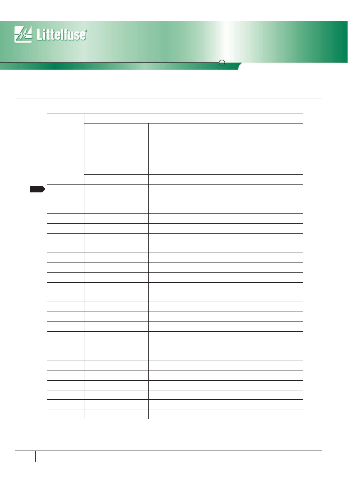
Device Ratings and Specifications
(Continued)
V18MLA0603 18 14 30 0.1 40 at 2A 22 28.0 125
V18MLA0402 18 14 20 0.050 40 at 1A 22 28.0 40
V18MLA0805 18 14 120 0.3 40 at 5A 22 28.0 450
V18MLA0805L 18 14 40 0.1 40 at 2A 22 28.0 250
V18MLA1206 18 14 150 0.4 40 22 28.0 1100
V18MLA1210 18 14 500 2.5 40 22 28.0 1250
V26MLA0603 26 20 30 0.1 58 at 2A 31 38 90
V26MLA0805 26 20 100 0.3 58 at 5A 29.5 38.5 190
V26MLA0805L 26 20 40 0.1 58 at 2A 29.5 38.5 115
V26MLA1206 26 20 150 0.6 56 29.5 38.5 900
V26MLA1210 26 20 300 1.2 54 29.5 38.5 1000
V30MLA0603 30 25 30 0.1 65 at 2A 37 46 75
V30MLA0805L 30 25 30 0.1 65 at 2A 37 46 80
V30MLA1210 30 25 280 1.2 62 35 43 1575
V30MLA1210L 30 25 220 0.9 62 35 43 1530
V33MLA1206 33 26 180 0.8 72 38 49 550
V42MLA1206 42 30 180 0.8 86 46 60 550
V48MLA1210 48 40 250 1.2 100 54.5 66.5 450
V48MLA1210L 48 40 220 0.9 100 54.5 66.5 430
V56MLA1206 56 40 180 1.0 110 61 77 150
V60MLA1210 60 50 250 1.5 120 67 83 375
V68MLA1206 68 50 180 1.0 130 76 90 150
V85MLA1210 85 67 250 2.5 160 95 115 225
V120MLA1210 120 107 125 2.0 230 135 165 65
NOTES:
1.
2.
3.
PA RT
NUMBER
MAXIMUM RATINGS (125
o
C) SPECIFICATIONS (25oC)
MAXIMUM
CONTINUOUS
WORKING
VO LTAGE
MAXIMUM
NON-
REPETITIVE
SURGE
CURRENT
(8/20µs)
MAXIMUM
NON-
REPETITIVE
SURGE
ENERGY
(10/1000µs)
MAXIMUM
CLAMPING
VO LTAG E AT
10A
(OR AS NOTED)
(8/20µs)
NOMINAL VOLTAGE
AT 1mA DC TEST
CURRENT
TYPICAL
CAPACITANCE
AT f = 1MHz
V
M(DC)VM(AC)
I
TM
W
TM
V
C
V
N(DC)
MIN
V
N(DC)
MAX C
(V) (V) (A) (J) (V) (V) (V) (pF)
L suffix is a low capacitance and energy version; Contact your Littelfuse Sales Representative for custom capacitance requirements.
Typical leakage at 25 C<25µA, maximum leakage 50µA at V ; for 0402 size, typical leakage <5µA, maximum leakage 10µA at V
o
M(DC)
M(DC).
Average power dissipation of transients for 0402, 0603, 0805, 1206 and 1210 sizes not to exceed 0.03W, 0.05W, 0.1W, 0.1W and 0.15W respectively.
NEW
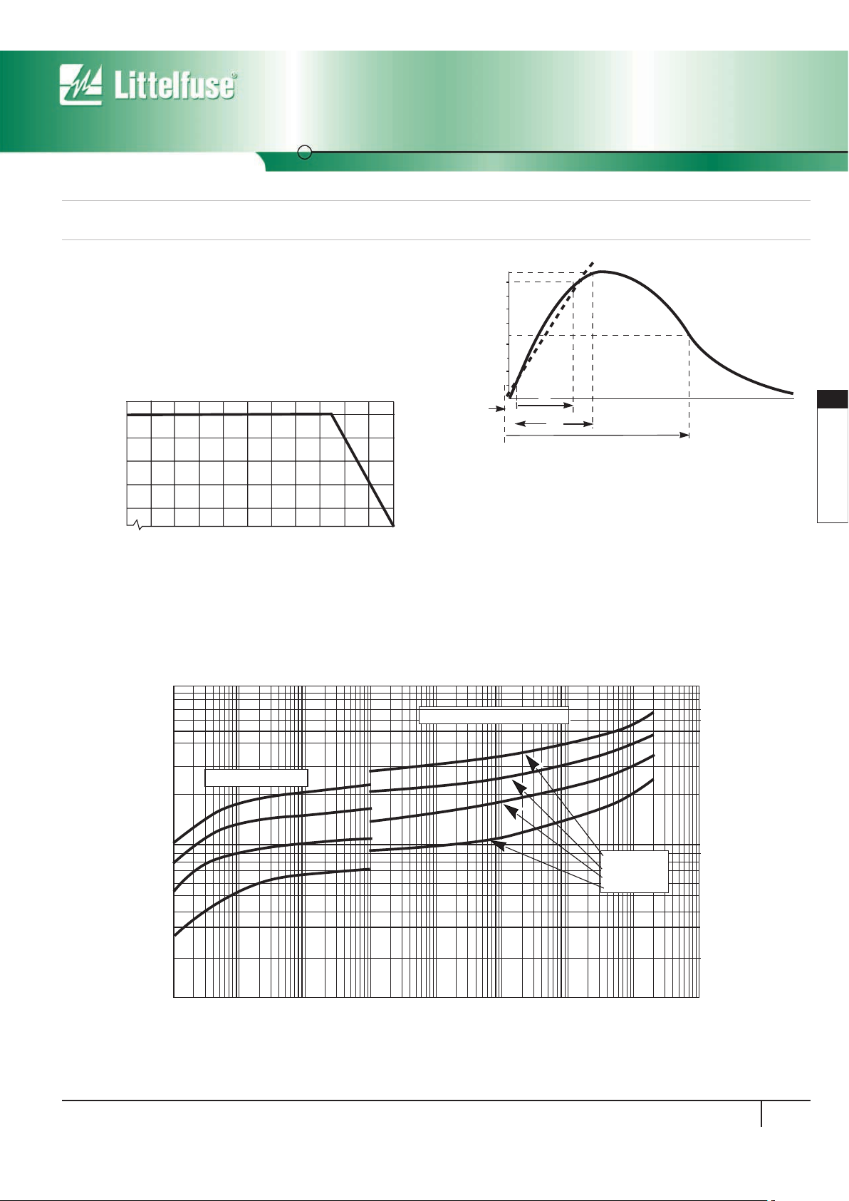
Temperature De-rating
When transients occur in rapid succession, the average power dissipation is the energy (watt-seconds) per pulse times the number of pulses
per second. The power so developed must be within the specifications
shown on the Device Ratings and Specifications table for the specific
device. For applications exceeding 125oC ambient temperature, the peak
surge current and energy ratings must be derated as shown in Figure 1.
100
80
60
40
20
0
-55 50 60 70 80 90 100 110 120 130 140 150
PERCENT OF RATED VALUE
AMBIENT TEMPERATURE (oC)
FIGURE 1. PEAK CURRENT AND ENERGY
DERATING CURVE
t
1
t
2
100
50
0
O
1
TIME
PERCENT OF PEAK VALUE
O1 = VIRTUAL ORIGIN OF WAVE
t
1
= VIRTUAL FRONT TIME = 1.25 x t
(IMPULSE DURATION)
t = TIME FROM 10% TO 90% OF PEAK
t
2
= VIRTUAL TIME TO HALF VALUE
EXAMPLE:
FOR AN 8/20µs CURRENT WAVEFORM
8µs = t
1
= VIRTUAL FRONT TIME
20µs = t
2
= VIRTUAL TIME TO
HALF VALUE
FIGURE 2. PEAK PULSE CURRENT TEST WAVEFORM
FOR CLAMPING VOLTAGE
t
FIGURE 3. LIMIT V-I CHARACTERISTIC FOR V5.5MLA0402 TO V18MLA0402
100
10
1µA
CURRENT (A)
Varistor Voltage (V)
MAXIMUM LEAKAGE
10µA 100 µA 1mA 10mA 100mA 1A 10A 100A
MAXIMUM CLAMPING VOLTAGE
V18MLA0402
V14MLA0402
V09MLA0402
V5.5MLA0402
ML Varistor Series
Surface Mount Varistors
Multilayer Transient Voltage Surge Suppressors
143
www.littelfuse.com
3
SURFACE MOUNT
VARISTORS
 Loading...