

Page 1
TVS Diode Arrays (SPA
I/O 1
I/O 2
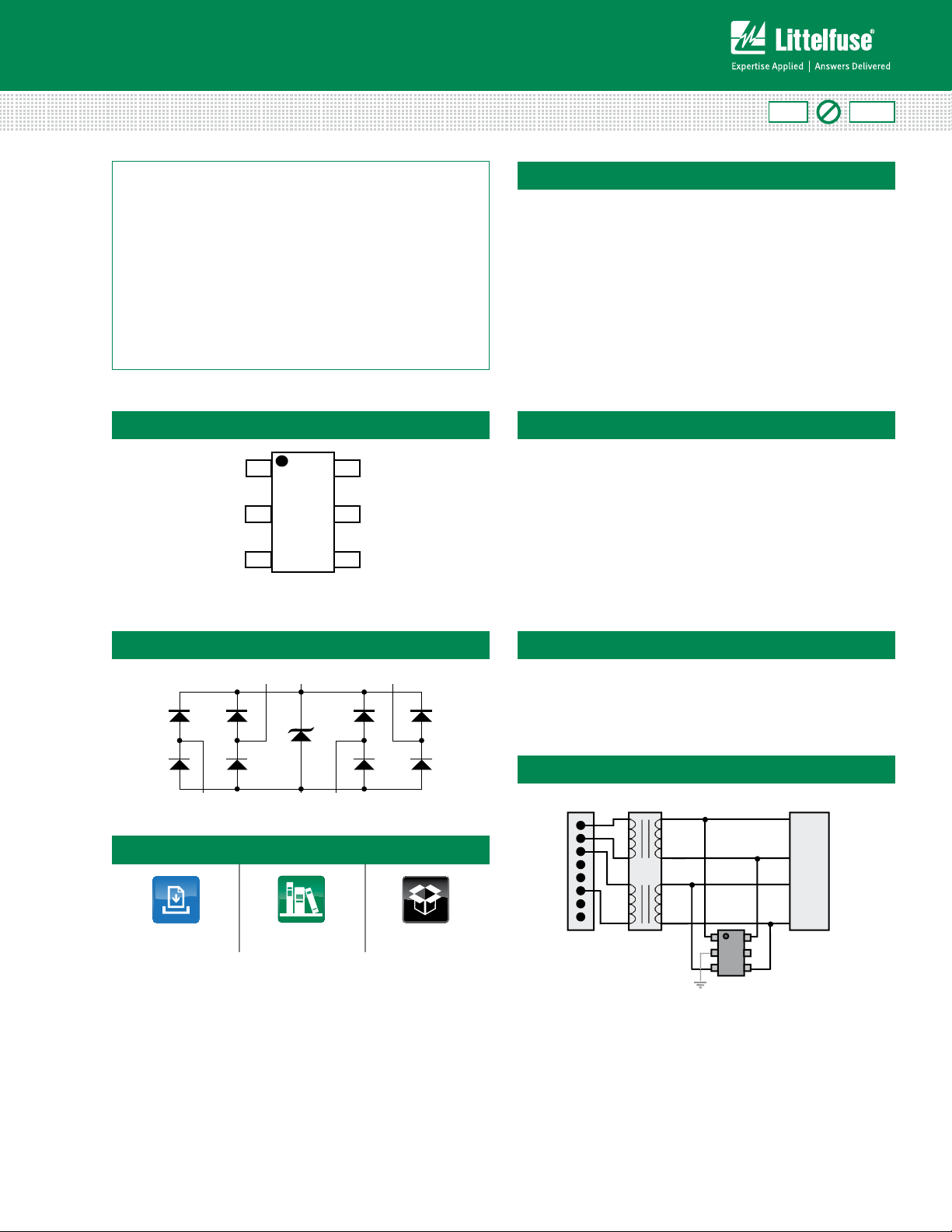
SOT23-6
V
CC
I/O 3
I/O 4
GND
RoHS
GREEN
RJ-45
®
Diodes)
Low Capacitance ESD Protection - SP0504S Series
SP0504S Series 0.85pF Diode Array
Pinout
Pb
Description
The SP0504S has ultra low capacitance rail-to-rail diodes
with an additional zener diode fabricated in a proprietary
silicon avalanche technology to protect each I/O pin
providing a high level of protection for electronic equipment
that may experience destructive electrostatic discharges
(ESD). These robust diodes can safely absorb repetitive
ESD strikes at the maximum level (Level 4) specified in the
IEC 61000-4-2 international standard without performance
degradation. Their very low loading capacitance also makes
them ideal for protecting high speed signal pins such as
HDMI, DVI, USB2.0, and IEEE 1394.
Features
• Low capacitance of
0.85 pF (TYP) per I/O
• ESD protection of
±12kV contact discharge,
±15kV air discharge,
(IEC61000-4-2)
• EFT protection,
IEC61000-4-4, 40A
(5/50ns)
• Low leakage current of
0.5μA (MAX) at 5V
• Small packaging options
saves board space
• Lightning Protection,
IEC61000-4-5, 4.5A
(8/20µs)
Functional Block Diagram
I/O4
I/O1
I/O2
V
CC
GND
I/O3
Additional Information
Datasheet
Life Support Note:
Not Intended for Use in Life Support or Life Saving Applications
The products shown herein are not designed for use in life sustaining or life saving
applications unless otherwise expressly indicated.
Resources
Samples
Applications
• Computer Peripherals
• Mobile Phones
• PDA’s
• Network Hardware/Ports
• Test Equipment
• Medical Equipment
• Digital Cameras
Application Example
Ethernet PHY
J1
J8
GND
SP0504S
Tx+
Tx-
Rx+
Rx-
NC
A single 4 channel SP0504S device can be used to protect
four of the data lines in a HDMI/DVI interface. Two (2)
SP0504S devices provide protection for the main data lines.
Low voltage ASIC HDMI/DVI drivers can also be protected
with the SP0504S, the +V
pins on the SP0504S can be
CC
substituted with a suitable bypass capacitor or in some
backdrive applications the +V
of the SP0504S can be
CC
oated or NC.
© 2013 Littelfuse, Inc.
Specifications are subject to change without notice.
Revised: 11/25/13
Page 2
TVS Diode Arrays (SPA
equency [Hz]
Insertion Loss [dB]
®
Diodes)
Low Capacitance ESD Protection - SP0504S Series
Absolute Maximum Ratings
Symbol Parameter Value Units
I
PP
T
OP
T
STOR
CAUTION: Stresses above those listed in “Absolute Maximum Ratings” may cause
permanent damage to the device. This is a stress only rating and operation of the device
at these or any other conditions above those indicated in the operational sections of this
specification is not implied.
Electrical Characteristics (T
Reverse Standoff Voltage V
Reverse Leakage Current I
Clamp Voltage
ESD Withstand Voltage
Diode Capacitance
Diode Capacitance
Note: 1. Parameter is guaranteed by design and/or device characterization.
Peak Current (tp=8/20μs) 4.5 A
Operating Temperature –40 to 125 °C
Storage Temperature –55 to 150 °C
=25ºC)
OP
Parameter Symbol Test Conditions Min Typ Max Units
RWM
LEAK
1
1
1
1
V
C
I/O-GND
C
V
C
ESD
I/O-I/O
IR ≤ 1µA 6.0 V
VR=5V 0.5 µA
IPP=1A, tp=8/20µs, Fwd 9.5 11. 0 V
I
=2A, tp=8/20µs, Fwd 10.6 13.0 V
PP
IEC61000-4-2 (Contact) ±12 kV
IEC61000-4-2 (Air) ±15 kV
Reverse Bias=0V 0.95 1. 1 1.25 pF
Reverse Bias=1.65V 0.7 0.85 1. 0 pF
Reverse Bias=0V 0.5 pF
Thermal Information
Parameter Rating Units
Storage Temperature Range –55 to
Maximum Junction Temperature 150 °C
Maximum Lead Temperature
(Soldering 20-40s)
150
260 °C
°C
0
-5
-10
-15
-20
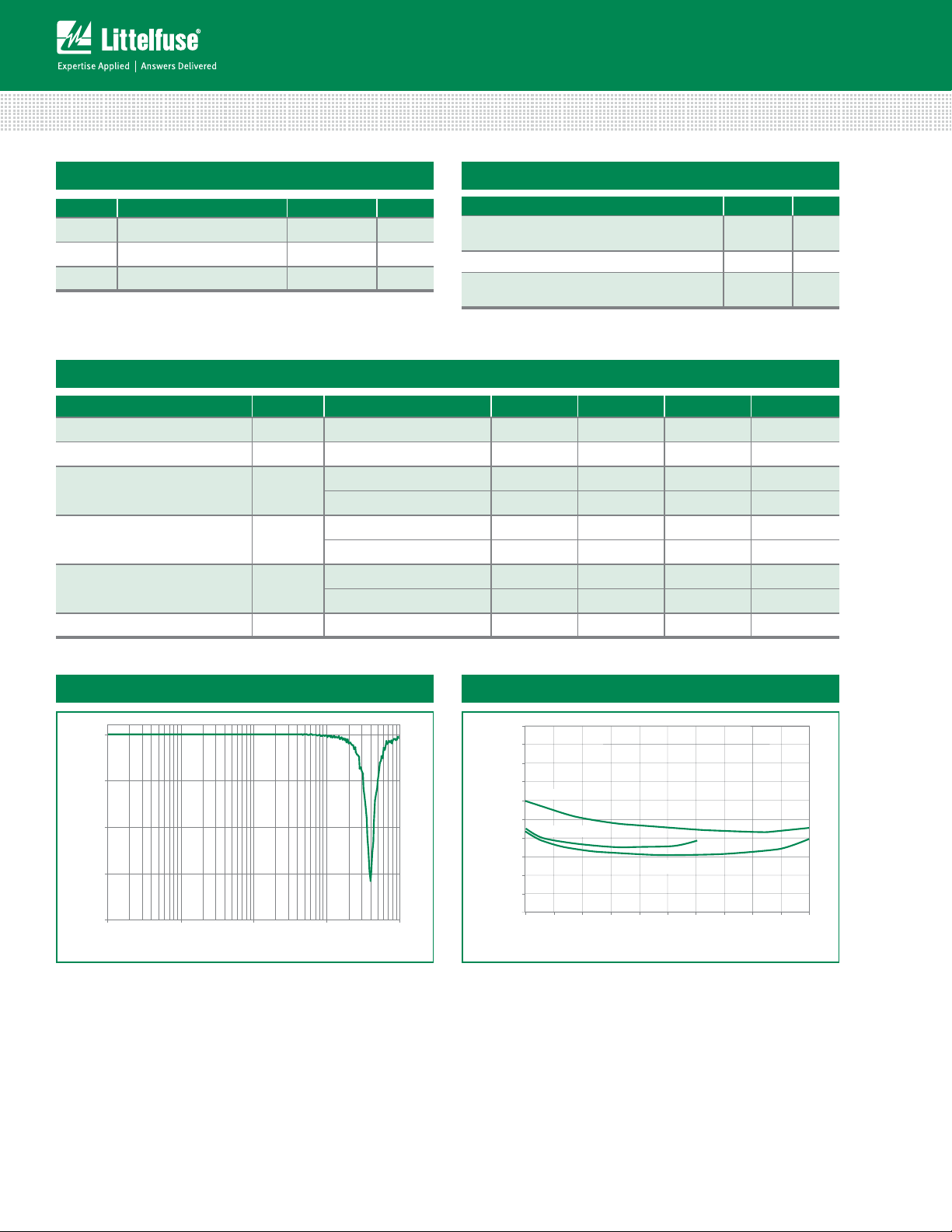
1.E+06 1.E+07 1.E+08 1.E+09 1.E+10
Fr
Capacitance vs. Bias VoltageInsertion Loss (S21) I/O to GND
1.50
1.40
1.30
1.20
1.10
1.00
0.90
0.80
I/O Capacitance (pF)
0.70
0.60
0.50
0.0 0.5 1.01.5 2.0 2.5 3.0 3.5 4.0 4.5 5.0
V
CC
= Float
VCC = 3.3V
VCC = 5V
I/O DC Bias (V)
Specifications are subject to change without notice.
© 2013 Littelfuse, Inc.
Revised: 11/25/13
Page 3

TVS Diode Arrays (SPA
Capacitance [F]
t
R
R
o
C
e
T
L
T
P
®
Diodes)
Low Capacitance ESD Protection - SP0504S Series
Capacitance vs. Frequency
2E-12
1.8E-12
1.6E-12
1.4E-12
1.2E-12
1E-12
8E-13
6E-13
4E-13
2E-13
0
1.E+06 1.E+07 1.E+08 1.E+09
Frequency [Hz]
Soldering Parameters
Reflow Condition Pb – Free assembly
- Temperature Min (T
Pre Heat
- Temperature Max (T
- Time (min to max) (ts) 60 – 180 secs
Average ramp up rate (Liquidus) Temp
(T
) to peak
L
to TL - Ramp-up Rate 3°C/second max
T
S(max)
Reflow
- Temperature (TL) (Liquidus) 217°C
- Temperature (tL) 60 – 150 seconds
Peak Temperature (TP) 260
Time within 5°C of actual peak
Temperature (t
)
p
Ramp-down Rate 6°C/second max
Time 25°C to peak Temperature (T
Do not exceed 260°C
) 150°C
s(min)
) 200°C
s(max)
3°C/second max
+0/-5
°C
20 – 40 seconds
) 8 minutes Max.
P
Product Characteristics
Lead Plating Matte Tin
Lead Material Copper Alloy
Lead Coplanarity 0.0004 inches (0.102mm)
Substitute Material Silicon
Body Material Molded Epoxy
Flammability UL 94 V-0
Notes :
1. All dimensions are in millimeters
2. Dimensions include solder plating.
3. Dimensions are exclusive of mold flash & metal burr.
4. Blo is facing up for mold and facing down for trim/form, i.e. reverse trim/form.
5. Package surface matte finish VDI 11-13.
t
T
P
Ramp-up
t
amp-up
PreheatPrehea
S
T
L
T
S(max)
Temperature
T
S(min)
25
time to peak temperature
P
t
L
Critical Zone
ritical Zon
L to TP
to
T
Ramp-down
amp-d
Time
Ordering Information
Part Number Package Marking Min. Order
SP0504SHTG SOT23-6 E*4 3000
Qty.
Part Numbering System
SP0504S
TVS Diode Arrays
®
(SPA
Diodes)
Series
© 2013 Littelfuse, Inc.
Specifications are subject to change without notice.
Revised: 11/25/13
H
TG
G= Green
T= Tape & Reel
Package
H = SOT23-6
Part Marking System
E*4
Product Series
E = SP0504S series
*
4
E
Assembly Site
(varies)
Number of Channels
Page 4

Package Dimensions — SOT23-6
Recommended Solder Pad Layout
TVS Diode Arrays (SPA
®
Diodes)
Low Capacitance ESD Protection - SP0504S Series
Package SOT23
Pins 6
JEDEC MO-178AB
Millimeters Inches
Min Max Min Max
A 0.900 1.450 0.035 0.057 -
A1 0.000 0.150 0.000 0.006 -
A2 0.900 1.300 0.035 0.051 -
b 0.350 0.500 0.0138 0.0196 -
C 0.080 0.220 0.0031 0.009 -
D 2.800 3.000 0.11 0.118 3
E 2.600 3.000 0.102 0.118 -
E1 1.500 1.750 0.06 0.069 3
e 0.95 Ref 0.0374 ref -
e1 1.9 Ref 0.0748 Ref -
L 0.30 0.600 0.012 0.023 4,5
N 6 6 6
a
M 2.590 0.102 -
O 0.690 .027 TYP -
P 0.990 .039 TYP -
R 0.950 0.038 -
Notes:
1. Dimensioning and tolerancing Per ASME Y14.5M-1994.
2. Package conforms to EIAJ SC-74 (1992).
3. Dimensions D and E1 are exclusive of mold flash, protrusions, or gate burrs.
4. Foot length L measured at reference to seating plane.
5. “L” is the length of flat foot surface for soldering to substrate.
6. “N” is the number of terminal positions.
M
7. Controlling dimension: MILLIMETER. Converted inch dimensions are not necessarily exact.
0º 8º 0º 8º -
Notes
P
R
O
Embossed Carrier Tape & Reel Specification — SOT23-6
8mm TAPE AND REEL
ACCESS HOLE
180mm
14.4mm
13mm
60mm
8.4mm
DIA. HOLE
8mm
1.5mm
SOT-23 (8mm POCKET PITCH)
USER DIRECTION OF FEED
4.0mm
4.0mm
2.0mm
1.75mm
C
L
GENERAL INFORMATION
1. 3000 PIECES PER REEL.
2. ORDER IN MULTIPLES OF FULL REELS ONLY.
3. MEETS EIA-481 REVISION "A" SPECIFICATIONS.
PIN 1
Specifications are subject to change without notice.
© 2013 Littelfuse, Inc.
Revised: 11/25/13
 Loading...