

Page 1
TVS Diode Arrays (SPA
RoHS
GREEN
®
Diodes)
General Purpose ESD Protection - SM05 through SM36
SM Series 400W TVS Diode Array
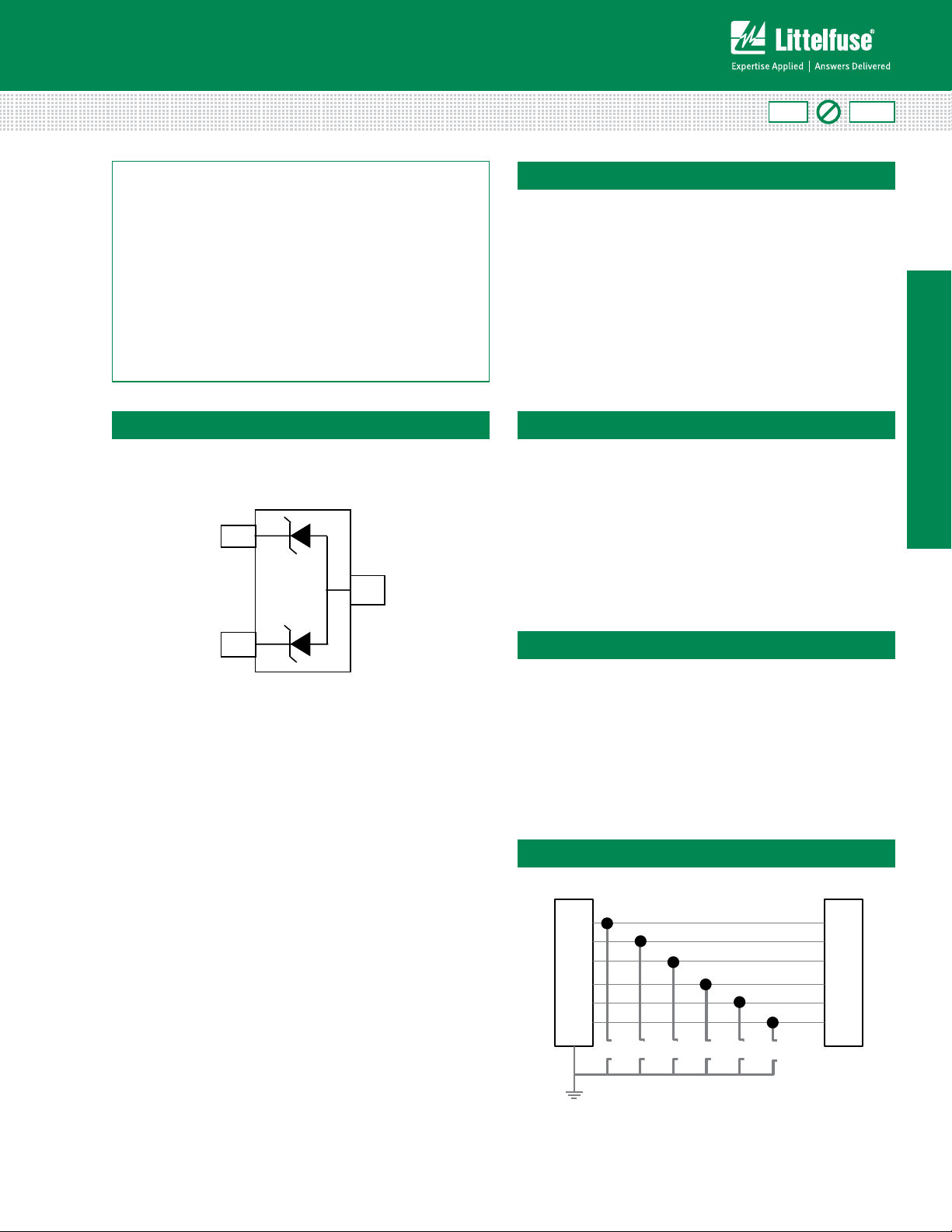
Pinout and Functional Block Diagram
(AEC-Q101 qualied)
1
Pb
Description
The SM series TVS Diode Array is designed to protect
sensitive equipment from damage due to electrostatic
discharge (ESD), electrical fast transients (EFT), and
lightning induced surges.
The SM series can absorb repetitive ESD strikes above the
maximum level specified in the IEC61000-4-2 international
standard without performance degradation and safely
dissipate up to 24A of 8/20us induced surge current (IEC61000-4-5) with very low clamping voltages.
Features
• ESD, IEC61000-4-2,
±30kV contact, ±30kV air
• EFT, IEC61000-4-4, 50A
(5/50ns)
• Lightning, IEC61000-4-5,
24A (t
=8/20μs, SM05)
P
• Working voltages: 5V,
12V, 15V, 24V and 36V
• Low clamping voltage
• Low leakage current
• AEC-Q101 qualied
(SOT23-3 package)
SM Series
3
2
Life Support Note:
Not Intended for Use in Life Support or Life Saving Applications
The products shown herein are not designed for use in life sustaining or life saving
applications unless otherwise expressly indicated.
Applications
• Industrial Equipment
• Test and Medical
Equipment
• Point-of-Sale Terminals
• Motor Controls
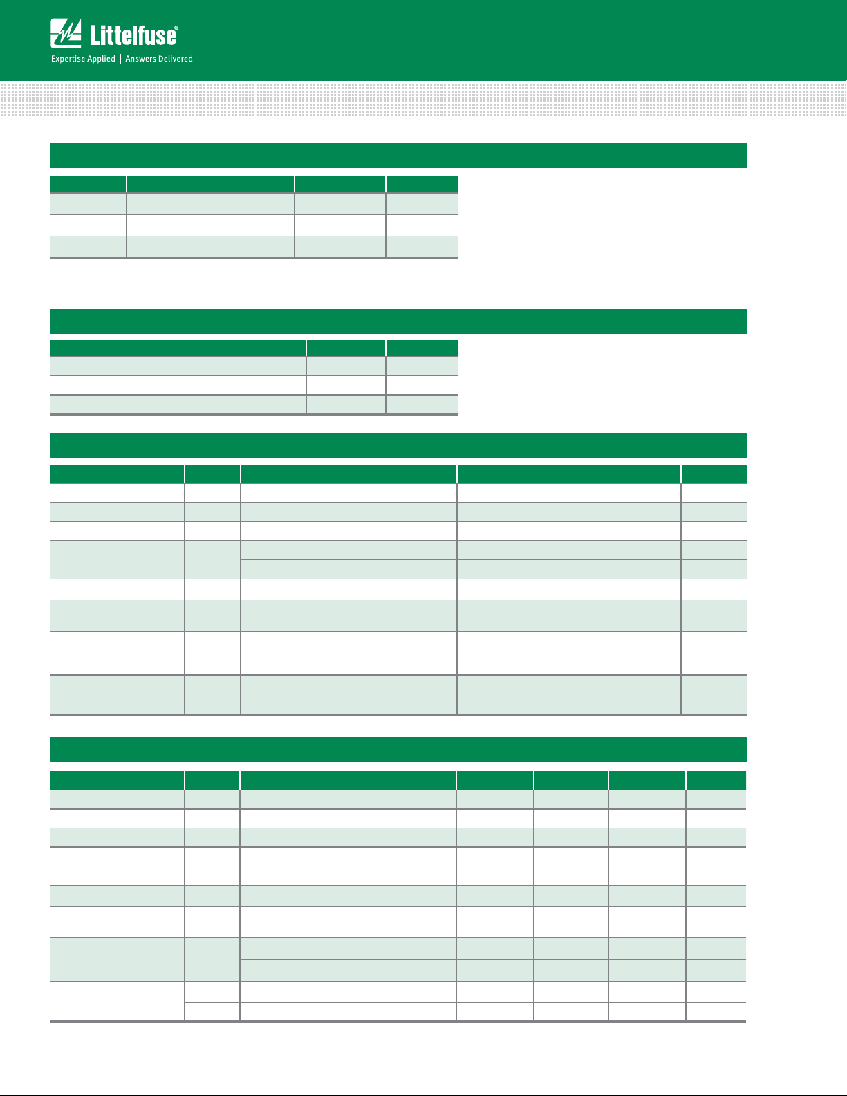
RS-232 Application Example
RS-232 Port
RD
TD
RTS
CTS
DSR
DTR
• Legacy Ports
(RS-232, RS-485)
• Security and Alarm
Systems
Transceiver
IC
© 2013 Littelfuse, Inc.
Specifications are subject to change without notice.
Revised: 12/05/13
Case GND
SM15 (x6)
(bidireconal implementaon)
5
Page 2
TVS Diode Arrays (SPA
®
Diodes)
General Purpose ESD Protection - SM05 through SM36
Absolute Maximum Ratings
Symbol Parameter Value Units
P
Pk
T
OP
T
STOR
Notes:
CAUTION: Stresses above those listed in “Absolute Maximum Ratings” may cause permanent damage to the device. This is a stress only rating and operation of
the device at these or any other conditions above those indicated in the operational sections of this specification is not implied.
Peak Pulse Power (tp=8/20μs)
Operating Temperature -40 to 125 °C
Storage Temperature -55 to 150 °C
Thermal Information
Parameter Rating Units
Storage Temperature Range -55 to 150 °C
Maximum Junction Temperature 150 °C
Maximum Lead Temperature (Soldering 20-40s) 260 °C
400
W
SM05 Electrical Characteristics (T
OP
=25ºC)
Parameter Symbol Test Conditions Min Typ Max Units
Reverse Standoff Voltage V
Reverse Voltage Drop V
Leakage Current I
Clamp Voltage
Dynamic Resistance
Peak Pulse Current
(8/20µs)
1
2
1
ESD Withstand Voltage
Diode Capacitance
1
RWM
R
LEAK
V
C
R
DYN
Ipp tp=8/20µs 24.0 A
1
V
ESD
C
I/O-GND
C
I/O-I/O
SM12 Electrical Characteristics (T
IPP=1A, tp=8/20µs, Pin 1 or Pin 2 to Pin 3 9.8 V
I
=10A, tp=8/20µs, Pin 1 or Pin 2 to Pin 3 13.0 V
PP
TLP, tp=100ns, I/O to GND 0.19 Ω
IEC61000-4-2 (Contact Discharge) ±30 kV
IEC61000-4-2 (Air Discharge) ±30 kV
Reverse Bias=0V, f=1MHz 400 pF
Reverse Bias=0V, f=1MHz 350 pF
=25ºC)
OP
IR≤1μA 5.0 V
IR=1mA 6.0 V
VR=5V 1. 0 μA
Parameter Symbol Test Conditions Min Ty p Max Units
Reverse Standoff Voltage V
Reverse Voltage Drop V
Leakage Current I
Clamp Voltage
Dynamic Resistance
Peak Pulse Current
(8/20µs)
ESD Withstand Voltage
Diode Capacitance
1
2
1
1
1
6
RWM
R
LEAK
V
R
IPP=1A, tp=8/20µs, Pin 1 or Pin 2 to Pin 3 18.5 V
C
I
=10A, tp=8/20µs, Pin 1 or Pin 2 to Pin 3 22.5 V
PP
DYN
TLP, tp=100ns, I/O to GND 0.25 Ω
Ipp tp=8/20µs 1 7. 0 A
V
C
C
ESD
I/O-GND
I/O-I/O
IEC61000-4-2 (Contact Discharge) ±30 kV
IEC61000-4-2 (Air Discharge) ±30 kV
Reverse Bias=0V, f=1MHz 150 pF
Reverse Bias=0V, f=1MHz 120 pF
IR≤1μA 12.0 V
IR=1mA 13.3 V
VR=12V 1. 0 μA
Specifications are subject to change without notice.
© 2013 Littelfuse, Inc.
Revised: 12/05/13
Page 3

TVS Diode Arrays (SPA
®
Diodes)
General Purpose ESD Protection - SM05 through SM36
SM15 Electrical Characteristics (T
OP
=25ºC)
Parameter Symbol Test Conditions Min Ty p Max Units
Reverse Standoff Voltage V
Reverse Voltage Drop V
Leakage Current I
Clamp Voltage
Dynamic Resistance
Peak Pulse Current
(8/20µs)
1
2
1
ESD Withstand Voltage
Diode Capacitance
1
RWM
R
LEAK
V
C
R
DYN
Ipp tp=8/20µs 12.0 A
1
V
ESD
C
I/O-GND
C
I/O-I/O
SM24 Electrical Characteristics (T
IPP=1A, tp=8/20µs, Pin 1 or Pin 2 to Pin 3 24.0 V
I
=10A, tp=8/20µs, Pin 1 or Pin 2 to Pin 3 30.0 V
PP
TLP, tp=100ns, I/O to GND 0.30 Ω
IEC61000-4-2 (Contact Discharge) ±30 kV
IEC61000-4-2 (Air Discharge) ±30 kV
Reverse Bias=0V, f=1MHz 100 pF
Reverse Bias=0V, f=1MHz 75 pF
=25ºC)
OP
IR≤1μA 15.0 V
IR=1mA 16.7 V
VR=15V 1. 0 μA
Parameter Symbol Test Conditions Min Ty p Max Units
Reverse Standoff Voltage V
Reverse Voltage Drop V
Leakage Current I
Clamp Voltage
Dynamic Resistance
Peak Pulse Current
(8/20µs)
ESD Withstand Voltage
Diode Capacitance
1
2
1
1
R
1
V
C
C
RWM
R
LEAK
V
IPP=1A, tp=8/20µs, Pin 1 or Pin 2 to Pin 3 36.0 V
C
I
=5A, tp=8/20µs, Pin 1 or Pin 2 to Pin 3 42.0 V
PP
DYN
TLP, tp=100ns, I/O to GND 0.50 Ω
Ipp tp=8/20µs 7. 0 A
IEC61000-4-2 (Contact Discharge) ±30 kV
ESD
I/O-GND
I/O-I/O
IEC61000-4-2 (Air Discharge) ±30 kV
Reverse Bias=0V, f=1MHz 65 pF
Reverse Bias=0V, f=1MHz 50 pF
IR≤1μA 24.0 V
IR=1mA 26.7 V
VR=24V 1. 0 μA
SM Series
SM36 Electrical Characteristics (T
OP
=25ºC)
Parameter Symbol Test Conditions Min Ty p Max Units
Reverse Standoff Voltage V
Reverse Voltage Drop V
Leakage Current I
Clamp Voltage
Dynamic Resistance
Peak Pulse Current
(8/20µs)
1
2
1
ESD Withstand Voltage
Diode Capacitance
Note:
1
Parameter is guaranteed by design and/or device characterization.
2
Transmission Line Pulse (TLP) with 100ns width and 200ps rise time.
© 2013 Littelfuse, Inc.
Specifications are subject to change without notice.
Revised: 12/05/13
1
RWM
R
LEAK
V
R
IPP=1A, tp=8/20µs, Pin 1 or Pin 2 to Pin 3 52.0 V
C
I
=4A, tp=8/20µs, Pin 1 or Pin 2 to Pin 3 62.0 V
PP
DYN
TLP, tp=100ns, I/O to GND 0.65 Ω
Ipp tp=8/20µs 5.0 A
1
V
ESD
C
I/O-GND
C
I/O-I/O
IEC61000-4-2 (Contact Discharge) ±30 kV
IEC61000-4-2 (Air Discharge) ±30 kV
Reverse Bias=0V, f=1MHz 50 pF
Reverse Bias=0V, f=1MHz 40 pF
IR≤1μA 36.0 V
IR=1mA 40.0 V
VR=36V 1. 0 μA
7
Page 4

TVS Diode Arrays (SPA
0%
10%
20%
30%
40%
50%
60%
70%
80%
90%
100%
110%
0.0 5.0 10.0 15.0 20.0 25.0 30.0
Time (μs)
Percent of I
PP
®
Diodes)
General Purpose ESD Protection - SM05 through SM36
Non-Repetitive Peak Pulse Power vs. Pulse Time
10
(kW)
pk
1
0.1
Peak Pulse Power - P
0.01
0.11 10 100 1000
Pulse Duration - tp (µs)
Pulse Waveform
Power Derating Curve
110
100
90
80
PP
70
60
50
40
30
20
% of Rated Power I
10
0
0255075100 125150
o
Ambient Temperature - T
(
C)
A
SM05 Transmission Line Pulsing(TLP) Plot
20
18
16
14
12
10
TLP Current (A)
8
6
4
2
0
024681012
SM05
TLP Voltage (V)
SM12 Transmission Line Pulsing(TLP) Plot
20
18
16
14
12
10
TLP Current (A)
8
8
6
4
2
0
0510 15 20 25
SM12
TLP Voltage (V)
SM15 Transmission Line Pulsing(TLP) Plot
20
18
16
14
12
10
TLP Current (A)
8
6
4
2
0
0510 15 20 25 30
SM15
TLP Voltage (V)
Specifications are subject to change without notice.
© 2013 Littelfuse, Inc.
Revised: 12/05/13
Page 5

TVS Diode Arrays (SPA
t
R
R
o
C
e
T
L
T
P
®
Diodes)
General Purpose ESD Protection - SM05 through SM36
SM24 Transmission Line Pulsing(TLP) Plot
20
18
16
14
12
10
TLP Current (A)
8
6
4
2
0
0510 15 20 25 30 35 40
SM24
TLP Voltage (V)
Soldering Parameters
Reflow Condition Pb – Free assembly
- Temperature Min (T
Pre Heat
- Temperature Max (T
- Time (min to max) (ts) 60 – 180 secs
Average ramp up rate (Liquidus) Temp
(T
) to peak
L
to TL - Ramp-up Rate 3°C/second max
T
S(max)
Reflow
- Temperature (TL) (Liquidus) 217°C
- Temperature (tL) 60 – 150 seconds
Peak Temperature (TP) 260
Time within 5°C of actual peak
Temperature (t
)
p
Ramp-down Rate 6°C/second max
Time 25°C to peak Temperature (T
Do not exceed 260°C
) 150°C
s(min)
) 200°C
s(max)
3°C/second max
+0/-5
°C
20 – 40 seconds
) 8 minutes Max.
P
SM36 Transmission Line Pulsing(TLP) Plot
t
S
SM36
TLP Voltage (V)
Ramp-up
PreheatPrehea
amp-up
t
P
t
L
20
18
16
14
12
10
TLP Current (A)
8
6
4
2
0
0510 15 20 25 30 35 40 45 50 55
T
P
T
L
T
S(max)
Temperature
T
S(min)
25
time to peak temperature
Product Characteristics
Critical Zone
ritical Zon
L to TP
to
T
Ramp-down
amp-d
Time
SM Series
Lead Plating
Matte Tin
Lead Material Copper Alloy
Ordering Information
Lead Coplanarity 0.0004 inches (0.102mm)
Part Number Package Marking Min. Order Qty.
SM05-02HTG SOT23-3 M05 3000
SM12-02HTG SOT23-3 M12 3000
SM15-02HTG SOT23-3 M15 3000
SM24-02HTG SOT23-3 M24 3000
SM36-02HTG SOT23-3 M36 3000
© 2013 Littelfuse, Inc.
Specifications are subject to change without notice.
Revised: 12/05/13
Substitute Material Silicon
Body Material Molded Epoxy
Flammability UL 94 V-0
Notes :
1. All dimensions are in millimeters
2. Dimensions include solder plating.
3. Dimensions are exclusive of mold flash & metal burr.
4. Blo is facing up for mold and facing down for trim/form, i.e. reverse trim/form.
5. Package surface matte finish VDI 11-13.
9
Page 6

TVS Diode Arrays (SPA
GENERAL INFORMATION
1. 3000 PIECES PER REEL.
2. ORDER IN MULTIPLES OF FULL REELS ONLY.
3. MEETS EIA-481 REVISION "A" SPECIFICATIONS.
USER DIRECTION OF FEED
PIN 1
SOT23-3 (8mm POCKET PITCH)
8.4mm
180mm
14.4mm
13mm
60mm
ACCESS HOLE
8mm TAPE AND REEL
P
b
0
N
M
xx
Mxx
®
Diodes)
General Purpose ESD Protection - SM05 through SM36
Part Marking System
Package Dimensions — SOT23-3
3
E
E1
2
D
A
A1
L1
Recommended Pad Layout
P
C
502B
1
e
e1
Part Numbering System
–
02
T
G
SM
TVS Diode Arrays
®
(SPA
Diodes)
Series
Working
Voltage
Number of
Channels
Package SOT23-3
Pins 3
JEDEC TO-236
Millimeters Inches
Min Max Min Max
A 0.89 1. 1 2 0.035 0.044
A1 0.01 0.1 0.0004 0.004
b 0.3 0.5 0.012 0.020
c 0.08 0.2 0.003 0.008
D 2.8 3.04 0.110 0.120
M
0
N
E 2.1 2.64 0.083 0.104
E1 1. 2 1. 4 0.047 0.055
e 0.95 BSC 0.038 BSC
e1 1.90 BSC 0.075 BSC
L1 0.54 REF 0.021 REF
M 2.29 .090
N 0.95 0.038
O 0.78 .030TYP
P 0.78 .030TYP
H
G= Green
T= Tape & Reel
Package
H: SOT23-3
Embossed Carrier Tape & Reel Specification — SOT23-3
10
Symbol
Millimetres Inches
Min Max Min Max
E 1.65 1.85 0.065 0.073
F 3.40 3.60 0.134 0.142
P2 1.90 2.10 0.075 0.083
D 1.40 1.60 0.055 0.063
P0 3.90 4.10 0.154 0.161
W 7.70 8.30 0.303 0.327
P 3.90 4.10 0.154 0.161
A0 3.05 3.25 0.120 0.128
B0 2.67 2.87 0.105 0.113
K0 1. 1 2 1.32 0.044 0.052
t 0.22 0.24 0.009 0.009
Specifications are subject to change without notice.
© 2013 Littelfuse, Inc.
Revised: 12/05/13
 Loading...