

Page 1
TVS Diode Arrays (SPA
5678
4321
Pin 1.3
Pin 2.4
Pin 6.8
Pin 5.7
RoHS
GREEN
®
Diodes)
Lightning Surge Protection - SLVU2.8-4 Series
SLVu2.8-4 Series 2.8V 40A TVS Array
Pinout
Pb
Description
The SLVU2.8-4 was designed to protect low voltage,
CMOS devices from ESD and lightning induced transients.
There is a compensating diode in series with each low
voltage TVS to present a low loading capacitance to the
line being protected. These robust structures can safely
absorb repetitive ESD strikes at ±30kV (contact discharge)
per IEC61000-4-2 standard and each structure can safely
dissipate up to 40A (IEC61000-4-5, t
low clamping voltages.
Features
• ESD, IEC61000-4-2,
±30kV contact, ±30kV air
• EFT, IEC61000-4-4, 40A
(5/50ns)
• Lightning, IEC61000-4-5,
40A (8/20μs)
• Low capacitance of 2pF
per line
=8/20μs) with very
P
• Low leakage current of
1μA (MAX) at 2.8V
• SOIC-8 (JEDEC MO-012)
pin configuration allows
for simple flow-through
layout
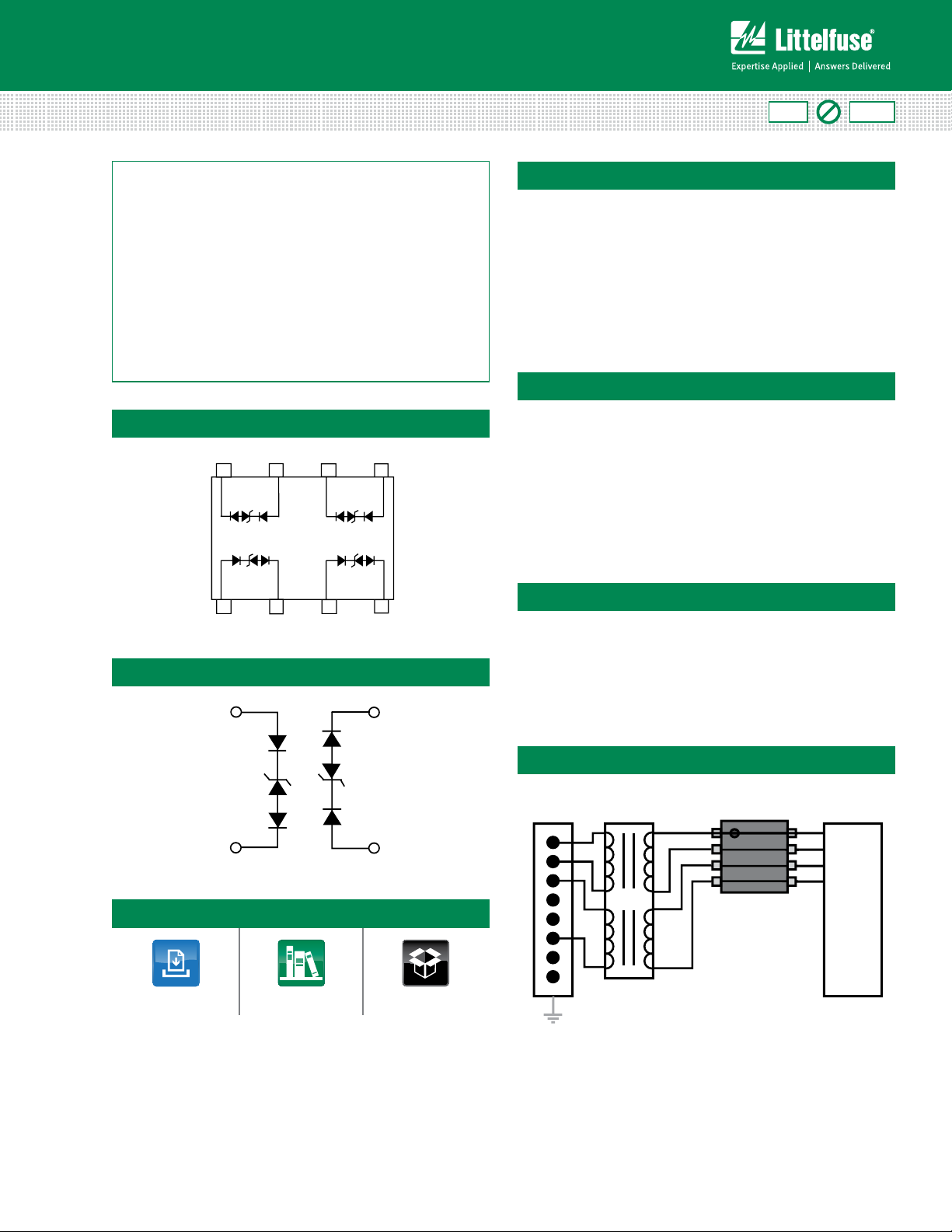
Functional Block Diagram
Additional Information
Datasheet
Resources
Samples
Applications
• 10/100/1000 Ethernet
• WAN/LAN Equipment
• Switching Systems
• Desktops, Servers, and
Notebooks
Application Example
RJ-45
Connector
J1
J8
Case GND
• Analog Inputs
• Base Stations
SLVU2.8-4
Device is shown
as transparent
for actual footprint
Ethernet
PHY
Tx+
TxRx+
Rx-
© 2013 Littelfuse, Inc.
Specifications are subject to change without notice.
Revised: 04/24/13
Page 2
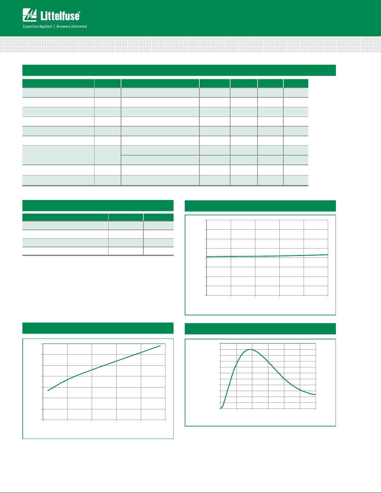
Electrical Characteristics (TOP = 25°C)
0.0
0.5
1.0
1.5
2.0
2.5
3.0
3.5
4.0
0.0 0.5 1.0 1.5 2.0 2.5
DC Bias (V)
Capacitance (pF)
0%
10%
20%
30%
40%
50%
60%
70%
80%
90%
100%
110%
0.0 5.0 10.0 15.0 20.0 25.0 30.0
Time (μs)
Percent of I
PP
0
2
4
6
8
10
12
14
0510 15 20 25
Peak Pulse Current-IPP (A)
Clamping Voltage-V
C
(V)
Parameter Symbol Test Conditions Min Typ Max Units
Reverse Standoff Voltage V
Reverse Breakdown Voltage V
Snap Back Voltage V
Reverse Leakage Current I
Clamping Voltage
Clamping Voltage
ESD Withstand Voltage
1
1
1
Dynamic Resistance R
Diode Capacitance
1
Note:
Parameter is guaranteed by design and/or device characterization.
1
V
RWM
BR
SB
LEAK
V
V
ESD
DYN
C
C
C
D
TVS Diode Arrays (SPA
®
Diodes)
Lightning Surge Protection - SLVU2.8-4 Series
IR≤1μA 2.8 V
IT=2μA 3.0 V
IT=50mA 2.8 V
VR=2.8V (Each Line) 1 μA
IPP=5A, tP=8/20μs (Each Line) 7. 0 8.5 V
IPP=24A, tP=8/20μs (Each Line) 13.9 15.0 V
IEC61000-4-2 (Contact) ±30 kV
IEC61000-4-2 (Air) ±30 kV
(VC2 - VC1) / (I
VR=0V, f=1MHz (Each Line)
- I
) (Each Line) 0.4 Ω
PP2
PP1
2.0 2.5 pF
Absolute Maximum Ratings
Parameter Rating Units
Peak Pulse Power (tP=8/20µs) 600 W
Peak Pulse Current (tP=8/20µs) 40 A
Operating Temperature –40 to 125 ºC
Storage Temperature –55 to 150 ºC
CAUTION: Stresses above those listed in “Absolute Maximum Ratings” may cause
permanent damage to the device. This is a stress only rating and operation of the device
at these or any other conditions above those indicated in the operational sections of this
specification is not implied.
Figure 2: Clamping Voltage vs. I
PP
Figure 1:
Capacitance vs. Reverse Voltage
Figure 3: Pulse Waveform
Specifications are subject to change without notice.
© 2013 Littelfuse, Inc.
Revised: 04/24/13
Page 3

TVS Diode Arrays (SPA
t
R
R
o
C
e
T
T
®
Diodes)
Lightning Surge Protection - SLVU2.8-4 Series
Product Characteristics
Lead Plating Matte Tin
Lead Material Copper Alloy
Lead Coplanarity 0.0004 inches (0.102mm)
Substitute Material Silicon
Body Material Molded Epoxy
Flammability UL 94 V-0
Notes :
1. All dimensions are in millimeters
2. Dimensions include solder plating.
3. Dimensions are exclusive of mold flash & metal burr.
4. All specifications comply to JEDEC SPEC MO-203 Issue A
5. Blo is facing up for mold and facing down for trim/form, i.e. reverse trim/form.
6. Package surface matte finish VDI 11-13.
Soldering Parameters
Reflow Condition Pb – Free assembly
- Temperature Min (T
Pre Heat
- Temperature Max (T
- Time (min to max) (t
Average ramp up rate (Liquidus) Temp
(T
) to peak
L
to TL - Ramp-up Rate 5°C/second max
T
S(max)
Reflow
- Temperature (T
- Temperature (t
Peak Temperature (T
L
) 60 – 150 seconds
L
) 260
P
Time within 5°C of actual peak
Temperature (t
)
p
Ramp-down Rate 5°C/second max
Time 25°C to peak Temperature (TP) 8 minutes Max.
Do not exceed 260°C
T
P
T
L
T
S(max)
t
PreheatPrehea
S
Temperature
T
S(min)
) 150°C
s(min)
) 200°C
s(max)
) 60 – 180 secs
s
5°C/second max
) (Liquidus) 217°C
+0/-5
20 – 40 seconds
t
P
Ramp-up
amp-up
t
L
°C
Critical Zone
ritical Zon
L to TP
to
T
Ramp-down
amp-d
25
time to peak temperature
Package Dimensions — Mechanical Drawings and Recommended Solder Pad Outline
Package SOIC-8
Pins 8
JEDEC MS-012
Millimetres Inches
L
o
F
Recommended
Soldering Pad Outline
(Reference Only)
A 1.35 1.75 0.053 0.069
A1 0.10 0.25 0.004 0.010
A2 1.25 1.65 0.050 0.065
B 0.31 0.51 0.012 0.020
c 0.17 0.25 0.007 0 .010
D 4.80 5.00 0.189 0.197
E 5.80
E1 3.80 4.00 0.150 0.157
e 1.27 BSC 0.050 BSC
L 0.40
Min Max Min Max
6.20
1.27
0.228
0.016
Time
0.244
0.050
© 2013 Littelfuse, Inc.
Specifications are subject to change without notice.
Revised: 04/24/13
Page 4

TVS Diode Arrays (SPA
SLVU2.8 B
T
G
Series
Package
B = SOIC-8
No. of channels
T= Tape & Reel
-4
G= Green
U2.8-4
U
2.8
Product Series
U = SLVU2.8
Voltage Level
-4
No. of channels
®
Diodes)
Lightning Surge Protection - SLVU2.8-4 Series
Part Numbering System
Embossed Carrier Tape & Reel Specification — SOIC Package
User Feeding Direction
Pin 1 Location
Part Marking System
Ordering Information
Part Number Package Marking Min. Order Qty.
SLVU2.8-4BTG SOIC-8 U2.8-4 2500
Symbol
E 1.65 1.85 0.065 0.073
F 5.4 5.6 0.213 0.22
P2 1.95 2.05 0.077 0.081
D 1. 5 1.6 0.059 0.063
D1 1.50 Min 0.059 Min
P0 3.9 4.1 0.154 0.161
10P0 40.0 ± 0.20 1.574 ± 0.008
W 11. 9 12.1 0.468 0.476
P 7. 9 8.1 0.311 0.319
A0 6.3 6.5 0.248 0.256
B0 5.1 5.3 0.2 0.209
K0 2 2.2 0.079 0.087
t 0.30 ± 0.05 0.012 ± 0.002
Millimetres Inches
Min Max Min Max
Specifications are subject to change without notice.
© 2013 Littelfuse, Inc.
Revised: 04/24/13
 Loading...