

TVS Diode Arrays (SPA
1
2
3
RoHS
GREEN
Ethernet
PHY
J1
J8
RJ-45
Connector
NC
NC
®
Diodes)
Lightning Surge Protection - SLVU2.8 Series
SLVu2.8 Series 2.8V 40A TVS Array
Pinout
Pb
Description
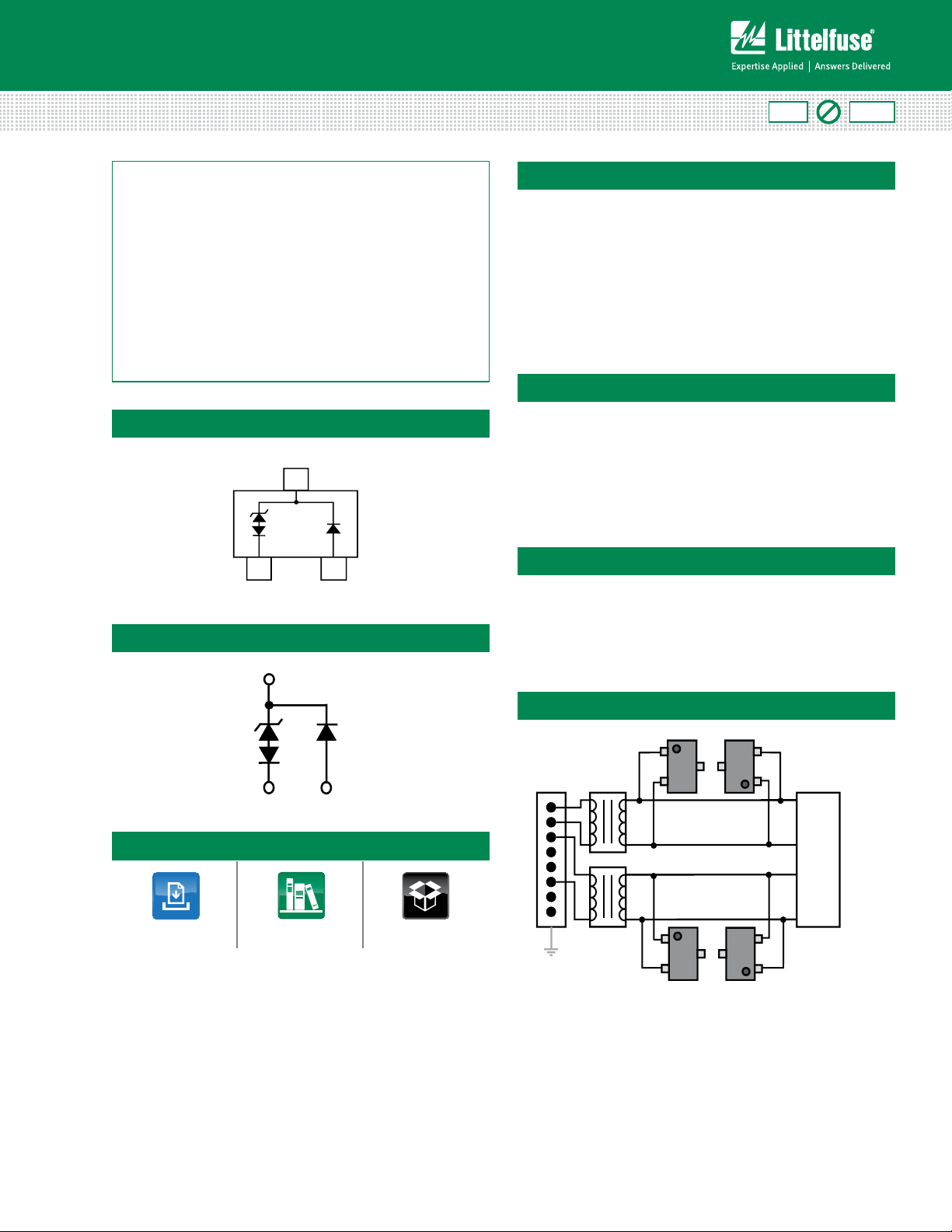
The SLVU2.8 series was designed to protect low voltage,
CMOS devices from ESD and lightning induced transients.
There is a compensating diode in parallel with the low
voltage TVS to protect one unidirectional line or a high
speed data pair when two devices are paired together.
These robust structures can safely absorb repetitive ESD
strikes at ±30kV (contact discharge) per the IEC61000-4-2
standard and each structure can safely dissipate up to 40A
(IEC61000-4-5, t
Features
• ESD, IEC61000-4-2,
±30kV contact, ±30kV air
• EFT, IEC61000-4-4, 40A
(5/50ns)
• Lightning, IEC61000-4-5,
40A (8/20μs)
Applications
=8/20μs) with very low clamping voltages.
P
• Low capacitance of 2pF
per line (Pin 2 to 1)
• Low leakage current of
1μA (MAX) at 2.8V
• Small SOT23-3 (JEDEC
TO-236) package saves
board space
Functional Block Diagram
Additional Information
Datasheet
Resources
• 10/100/1000 Ethernet
• WAN/LAN Equipment
• Analog Inputs
• Base Stations
• Switching Systems
• Desktops, Servers, and
3
Notebooks
Application Example
1
2
Samples
© 2013 Littelfuse, Inc.
Specifications are subject to change without notice.
Revised: 04/24/13
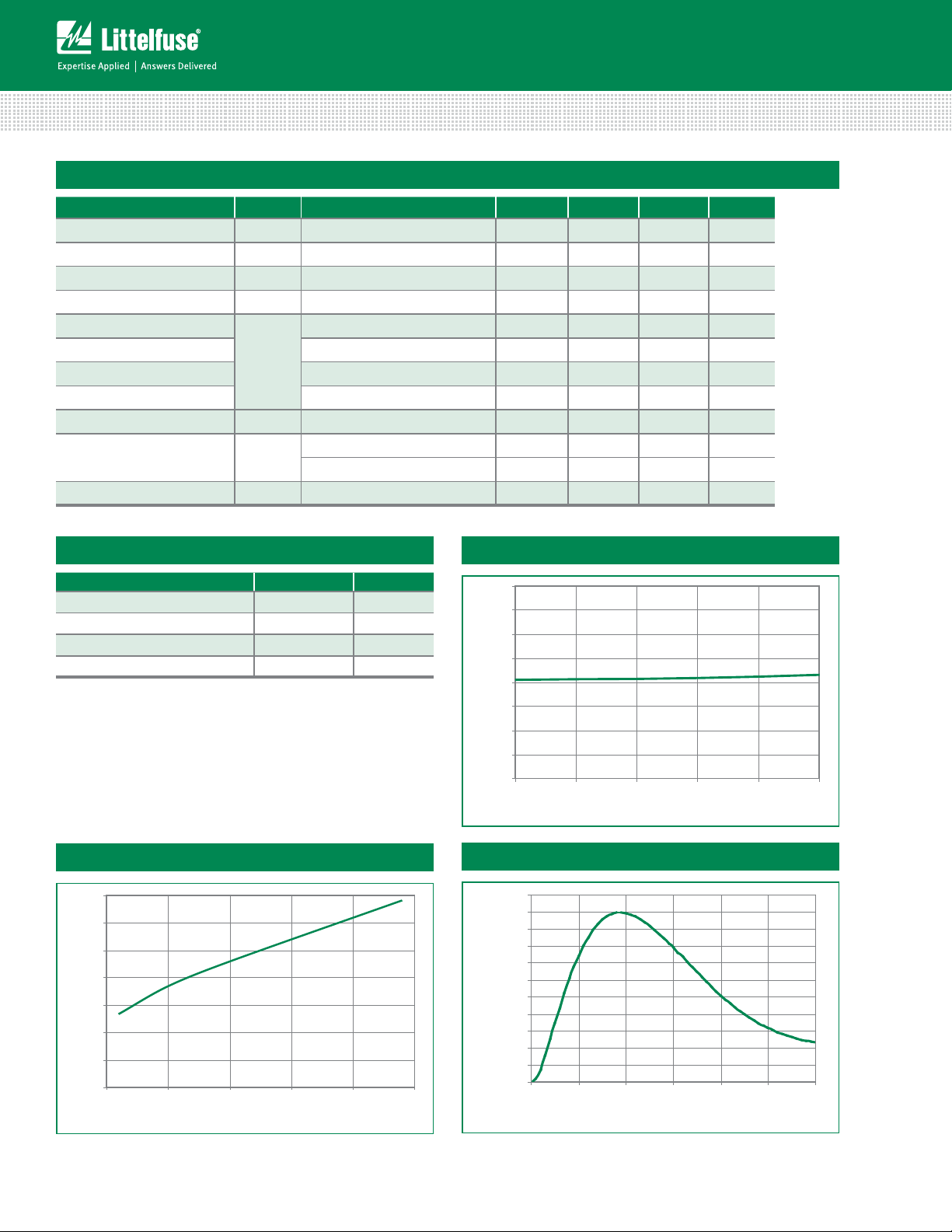
Electrical Characteristics (TOP = 25°C)
0.0
0.5
1.0
1.5
2.0
2.5
3.0
3.5
4.0
0.0 0.5 1.0 1.5 2.0 2.5
DC Bias (V)
Capacitance (pF)
0%
10%
20%
30%
40%
50%
60%
70%
80%
90%
100%
110%
0.0 5.0 10.0 15.0 20.0 25.0 30.0
Time (μs)
Percent of I
PP
0
2
4
6
8
10
12
14
0510 15 20 25
Peak Pulse Current-IPP (A)
Clamping Voltage-V
C
(V)
Parameter Symbol Test Conditions Min Typ Max Units
Reverse Standoff Voltage V
Reverse Breakdown Voltage V
Snap Back Voltage V
Reverse Leakage Current I
Clamping Voltage
Clamping Voltage
Clamping Voltage
Clamping Voltage
1
1
1
1
Dynamic Resistance R
ESD Withstand Voltage
Diode Capacitance
1
Note:
Parameter is guaranteed by design and/or device characterization.
1
1
V
RWM
BR
SB
LEAK
V
DYN
ESD
C
C
D
TVS Diode Arrays (SPA
®
Diodes)
Lightning Surge Protection - SLVU2.8 Series
IR≤1μA 2.8 V
IT=2μA 3.0 V
IT=50mA 2.8 V
VR=2.8V (Pin 2 or 3 to 1) 1 μA
IPP=5A, tP=8/20μs (Pin 3 to 1) 5.7 7. 0 V
IPP=24A, tP=8/20μs (Pin 3 to 1) 8.3 12.5 V
IPP=5A, tP=8/20μs (Pin 2 to 1) 7. 0 8.5 V
IPP=24A, tP=8/20μs (Pin 2 to 1) 13.9 15.0 V
(VC2 - VC1) / (I
IEC61000-4-2 (Contact) ±30 kV
VR=0V, f=1MHz (Pin 2 to 1)
- I
) (Pin 2 to 1) 0.4 Ω
PP2
PP1
IEC61000-4-2 (Air)
±30 kV
2.0 2.5 pF
Absolute Maximum Ratings
Parameter Rating Units
Peak Pulse Power (tP=8/20µs) 600 W
Peak Pulse Current (tP=8/20µs) 40 A
Operating Temperature –40 to 125 ºC
Storage Temperature –55 to 150 ºC
CAUTION: Stresses above those listed in “Absolute Maximum Ratings” may cause
permanent damage to the device. This is a stress only rating and operation of the device
at these or any other conditions above those indicated in the operational sections of this
specification is not implied.
Figure 2: Clamping Voltage vs. I
PP
Figure 1:
Capacitance vs. Reverse Voltage
Figure 3: Pulse Waveform
Specifications are subject to change without notice.
© 2013 Littelfuse, Inc.
Revised: 04/24/13
 Loading...