

Page 1
Transient Voltage Suppression Diodes
Surface Mount – 500W > SACB series
SACB Series
Uni-directional
Agency Approvals
AGENCY AGENCY FILE NUMBER
E230531
Maximum Ratings and Thermal Characteristics
(T
=25°C unless otherwise noted)
A
Parameter Symbol Value Unit
Peak Pulse Power Dissipation at
ta=25°C by 10/1000μs Waveform
(g.1)( Note 1)
Power Dissipation on Innite Heat
Sink at TL=50ºC
Peak Pulse Power Dissipation at
Ta=25ºC by 10/1000μs Waveform
(Fig. 3) (Note 1)
Operating Junction and Storage
Temperature Range
Typical Thermal Resistance Junction
to Lead
Typical Thermal Resistance Junction
to Ambient
Note:
1. Non-repetitive current pulse , per Fig. 3 and derated above T
P
PPM
P
M(AV)
I
PPM
, T
T
J
R
uJL
R
uJA
500 W
3.0 W
See
Table 1
-55 to 150 °C
STG
30 °C/W
120 °C/W
= 25°C per Fig. 2.
A
Amps
RoHS
Description
SACB series is designed specifically to protect sensitive
electronic equipment from voltage transients induced by
lightning and other transient voltage events.
Features
• For surface mounted
applications in order to
optimize board space
• Low prole package
• Built-in strain relief
• Typical failure mode is
short from over-specied
voltage or current
• Whisker test is conducted
based on JEDEC
JESD201A per its table 4a
and 4c
• IEC-61000-4-2 ESD
15kV(Air), 8kV (Contact)
• ESD protection of data
lines in accordance with
IEC 61000-4-2 (IEC801-2)
• EFT protection of data
lines in accordance with
IEC 61000-4-4 (IEC801-4)
•
VBR @TJ= VBR@25°C × (1+αT
x (TJ - 25))
(αT: Temperature Coefcient)
• Glass passivated chip
• 500W peak pulse power
capability at 10/1000μs
waveform, repetition rate
(duty cycles):0.01%
• Fast response time:
typically less than 1.0ps
from 0V to BV min
• Excellent clamping
capability
• Low incremental surge
resistance
• High temperature
soldering guaranteed:
260°C/40 seconds at
terminals
• Plastic package has
underwriters laboratory
ammability 94V-O
• Meet MSL level1, per
J-STD-020, LF maximum
peak of 260°C
• Matte tin lead–free plated
• Halogen free and RoHS
compliant
junction
Applications
TVS devices are ideal for the protection of I/O Interfaces,
V
bus and other vulnerable circuits used in Telecom,
CC
Computer, Industrial and Consumer electronic applications.
Additional Information
Datasheet
Resources
Specifications are subject to change without notice.
Samples
© 2014 Littelfuse, Inc.
Revised: 01/20/14
Page 2
Transient Voltage Suppression Diodes
0.1µ
1.0µ
10µs
100µs
1.0ms
10ms
Non-repetitive Pulse
Current Waveforms
Square
P
td=7tp
td
td
P
Half Sine
Impulse
td
P
Exponential
Decay
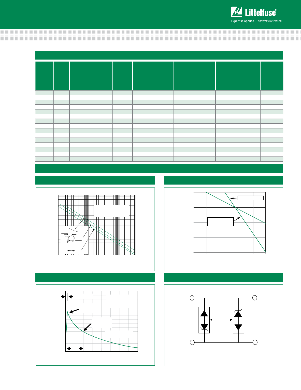
SACB: Revised Figure 1 - Peak Pulse Power Rating Curve
Surface Mount – 500W > SACB series
Electrical Characteristics (T
Stand-Off
Part
Number
Marking
Code
Voltage
(Note1) V
(V)
=25°C unless otherwise noted)
A
BR
Maximum
Reverse
Leakage
at V
(V)
Minimum
Breakdown
Voltage at
R
=1.0MA
I
T
V
A)
R IR
Maximum
Clamping
Voltage at
I
=5.0A
PP
V
C
(V)
Maximum
Peak
Pulse
Current
per (Fig.3)
(A)
I
PP
Maximum
Junction
Capacitance
at
0 Volts (pF)
Working
Inverse
Blocking
Voltage
V
(V)
WIB
Inverse
Blocking
Leakage
Current at
@ I
V
WIB
IB
(mA)
Peak Inverse
Blocking
Voltage V
(V)
PIB
Recognition
SACB5.0 SKE 5.0 7.60 300 10.0 44.0 45 75 1.0 100 X
SACB6.0 SKG 6.0 7.90 300 11.2 41.0 45 75 1.0 100 X
SACB7.0 SKM 7.0 8.33 300 12.6 38.0 45 75 1.0 100 X
SACB8.0 SKR 8.0 8.89 100 13.4 36.0 45 75 1.0 100 X
SACB8.5 SKT 8.5 9.44 50 14.0 34.0 45 75 1.0 100 X
SACB10 SKX 10.0 11.10 5 16.3 29.0 45 75 1.0 100 X
SACB12 SLE 12.0 13.30 5 19.0 25.0 45 75 1.0 100 X
SACB15 SLM 15.0 16.70 5 23.6 20.0 45 75 1.0 100 X
SACB18 SLT 18.0 20.00 5 28.8 15.0 45 75 1.0 100 X
SACB22 SLX 22.0 24.40 5 35.4 14.0 45 75 1.0 100 X
SACB26 SME 26.0 28.90 5 42.3 11.1 45 75 1.0 100 X
SACB30 SMK 30.0 33.30 5 48.6 10.0 45 75 1.0 100 X
SACB36 SMP 36.0 40.00 5 60.0 8.6 45 75 1.0 100 X
SACB45 SMV 45.0 50.00 5 77.0 6.8 45 150 1.0 200 X
SACB50 SMZ 50.0 55.50 5 88.0 5.8 45 150 1.0 200 X
Ratings and Characteristic Curves (T
Ratings and Characteristic Curves (T
=25°C unless otherwise noted
= 25°C unless otherwise noted)
A
A
Figure 1 - Peak Pulse Power Rating Curve Figure 2 - Pulse Derating Curve
100
30
10
- Peak Pulse Power (kW)
".5"
PK
1
PPM
I
PK
PK
0.1
s
s
Waveform shown in Fig. 3
T
=25°C
A
td - Pulse Width (sec.)
100
Average Power
75
50
Peak Power
(Single Pulse)
25
Percentage of Rated Power (%)
0
0255075100 125 150
TL - Lead Temperature (ºC)
UL
Figure 3 - Pulse Waveform
150
RSM
100
50
- Peak Pulse Current, % I
PPM
I
0
© 2014 Littelfuse, Inc.
Specifications are subject to change without notice.
Revised: 01/20/14
tr=10µsec
Peak Value
I
PPM
t
d
0
1.0 2.0 3.0 4.0
Half Value
I
PPM
I
PPM
( )
2
10/1000µsec. Waveform
as defined by R.E.A
t-Time (ms)
TJ=25°C
Pulse Width(td) is defined
as the point where the peak
current decays to 50% of I
PPM
Figure 4 - AC Line Protection Application
Low Capacitance
Application Note: Device must be used with two
units in parallel, opposite in polarity as shown in
circuit for AC signal line protection.
Page 3

Soldering Parameters
Transient Voltage Suppression Diodes
Surface Mount – 500W > SACB series
Reflow Condition Lead–free assembly
Pre Heat
- Temperature Min (T
- Temperature Max (T
) 150°C
s(min)
) 200°C
s(max)
- Time (min to max) (ts) 60 – 180 secs
Average ramp up rate (Liquidus Temp
(T
) to peak
L
to TL - Ramp-up Rate 3°C/second max
T
S(max)
Reflow
- Temperature (TL) (Liquidus) 217°C
- Time (min to max) (ts) 60 – 150 seconds
Peak Temperature (TP) 260
Time within 5°C of actual peak
Temperature (t
)
p
3°C/second max
+0/-5
°C
20 – 40 seconds
Ramp-down Rate 6°C/second max
Time 25°C to peak Temperature (T
) 8 minutes Max.
P
Do not exceed 280°C
Physical Specifications
Weight 0.003oz., 0.093g
Case
JEDEC DO-214AA molded plastic body
over glass passivated junction.
t
T
P
Ramp-up Critical Zone
T
L
T
s(max)
T
s(min)
Temperature (T)
25˚C
t
s
Preheat
t 25˚C to Peak
Time (t)
p
Flow/Wave Soldering (Solder Dipping)
Peak Temperature : 265OC
Dipping Time : 10 seconds
Soldering : 1 time
Environmental Specifications
High Temp. Storage JESD22-A103
HTRB JESD22-A108
T
T
to
L
t
L
P
Ramp-down
Polarity
Terminal
Dimensions
A
D
E
Color band denotes cathode except
Bidirectional
Matte Tin-plated leads. Solderable per
JESD22-B102.
DO-214AA (SMB J-Bend)
Cathode Band
B
F
G
Temperature Cycling JESD22-A104
MSL JEDEC-J-STD-020, Level 1
H3TRB JESD22-A101
RSH JESD22-B106
Dimensions
Inches Millimeters
Min Max Min Max
A 0.077 0.086 1.950 2.200
B 0.160 0.180 4.060 4.570
C
C 0.130 0.155 3.300 3.940
D 0.084 0.096 2.130 2.440
E 0.030 0.060 0.760 1.520
F - 0.008 - 0.203
H
G 0.205 0.220 5.210 5.590
H 0.006 0.012 0.152 0.305
Specifications are subject to change without notice.
© 2014 Littelfuse, Inc.
Revised: 01/20/14
Page 4

Transient Voltage Suppression Diodes
(for uni-directional products only)
0.47
(12.0)
0.315
(8.0)
0.157
(4.0)
0.49
(12.5)
0.80 (20.2)
Arbor Hole Dia.
13.0 (330)
Dimensions are in inches
(and millimeters).
Direction of Feed
0.059
DIA
(1.5)
Cover tape
Surface Mount – 500W > SACB series
Part Numbering System
SACB
Series Type
XX
Stand Off Voltage
Part Marking System
F
XX
YMXXX
Packaging
Part number
SACBXX DO-214AA 3000 Tape & Reel - 12mm tape/13” reel EIA STD RS-481
Component
Package
Quantity
Schematic
Packaging
Option
Packaging Specification
Cathode Band
Littelfuse Logo
Marking Code
Trace Code Marking
Y:Year Code
M: Month Code
XXX: Lot Code
Tape and Reel Specification
Transient
Voltage
Suppressor
Diode
Cathode
© 2014 Littelfuse, Inc.
Specifications are subject to change without notice.
Revised: 01/20/14
 Loading...