

Littelfuse Qxx12xHx User Manual
Qxx12xHx Series
Teccor® brand Thyristors
12 Amp Alternistor (High Communitation) Triacs
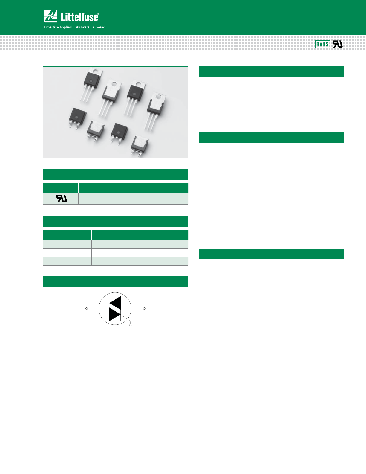
Description
12 Amp bi-directional solid state switch series is designed
for AC switching and phase control applications such as
motor speed and temperature modulation controls, lighting
controls, and static switching relays.
Alternistor type devices only operate in quadrants I, II, & III
and are used in circuits requiring high dv/dt capability.
Features & Benefits
Agency Approval
Agency Agency File Number
®
L Package: E71639
Main Features
Symbol Value Unit
I
T(RMS)
V
DRM/VRRM
I
GT (Q1)
12 A
400 to 1000 V
10 to 50 mA
Schematic Symbol
MT2 MT1
G
t3P)4$PNQMJBOU
t(MBTToQBTTJWBUFE
junctions
t7PMUBHFDBQBCJMJUZVQUP
1000 V
t4VSHFDBQBCJMJUZVQUP
120 A
t&MFDUSJDBMMZJTPMBUFE
“L-Package” is UL
recognized for 2500Vrms
t4PMJETUBUFTXJUDIJOH
contact bounce that
create voltage transients
t/PDPOUBDUTUPXFBS
out from reaction of
switching events
t3FTUSJDUFEPSMJNJUFE3'*
generation, depending
on activation point sine
wave
t3FRVJSFTPOMZBTNBMM
gate activation pulse in
each half-cycle
eliminates arcing or
Applications
Excellent for AC switching and phase control applications
such as heating, lighting, and motor speed controls.
Typical applications are AC solid-state switches, light
dimmers, power tools, lawn care equipment, home/brown
goods and white goods appliances.
Alternistor Triacs (no snubber required) are used in
applications with extremely inductive loads requiring
highest commutation performance.
Internally constructed isolated packages are offered for
ease of heat sinking with highest isolation voltage.
Qxx12xHx Series
107
Specifications are subject to change without notice.
©2013 Littelfuse, Inc
Revised: 09/23/13
Teccor® brand Thyristors
12 Amp Alternistor (High Communitation) Triacs
Absolute Maximum Ratings — Alternistor (3 Quadrants)
Symbol Parameter Value Unit
Qxx12LHy T
I
T(RMS)
RMS on-state current (full sine wave)
Qxx12RHy
Qxx12NHy
I
TSM
2
tI
I
Non repetitive surge peak on-state current
(full cycle, TJ initial = 25°C)
2
t Value for fusing tp = 8.3 ms 60 A2s
f = 50 Hz t = 20 ms 110
f = 60 Hz t = 16.7 ms 120
di/dt Critical rate of rise of on-state current f = 120 Hz
10 s;
t
I
GTM
P
G(AV)
T
stg
T
J
Note: xx = voltage, y = sensitivity
Operating junction temperature range -40 to 125 °C
Peak gate trigger current
Average gate power dissipation
Storage temperature range -40 to 150 °C
p
IGT I
GTM
= 90°C
C
= 105°C
T
C
= 125°C
T
J
= 125°C
T
J
T
= 125°C
J
12 A
70 A/s
2.0 A
0.5 W
A
Electrical Characteristics (T
= 25°C, unless otherwise specified) — Alternistor Triac (3 Quadrants)
J
Symbol Test Conditions Quadrant Qxx12xH2 Qxx12xH5 Unit
I
GT
V
GT
V
GD
I
H
dv/dt
VD = 12V RL = 60
VD = V
RL = 3.3 k TJ = 125°C *o**o*** MIN. 0.2 0.2 V
DRM
IT = 100mA MAX. 15 50 mA
VD = V
VD = V
Gate Open TJ = 125°C
DRM
Gate Open TJ = 100°C 1000V 150 300
DRM
*o**o*** MAX. 10 50 mA
*o**o*** MAX. 1.3 1.3 V
400V
600V 200 650
800V 150 500
MIN.
300 750
V/s
(dv/dt)c (di/dt)c = 6.5 A/ms TJ = 125°C MIN. 2 30 V/s
t
gt
IG = 2 x IGT PW = 15s IT = 17.0 A(pk) TYP. 4 4 s
Static Characteristics
Symbol Test Conditions Value Unit
V
I
I
TM
DRM
RRM
ITM = 17.0A tp = 380 µs MAX. 1.60 V
VD = V
DRM
/ V
RRM
TJ = 25°C 400-1000V
= 125°C 400-800V 2
T
J
= 100°C 1000V 3
T
J
MAX.
10 A
mA
Thermal Resistances
Symbol Parameter Value Unit
R
(J-C)
R
(J-A)
Note: xx = voltage, y = sensitivity
Qxx12xHx Series
Junction to case (AC)
Junction to ambient (AC)
Qxx12RHy
Qxx12NHy
Qxx12LHy 2.3
Qxx12RHy 45
Qxx12LHy 90
108
1. 2
Specifications are subject to change without notice.
°C/W
°C/W
©2013 Littelfuse, Inc
Revised: 09/23/13
Teccor® brand Thyristors
12 Amp Alternistor (High Communitation) Triacs
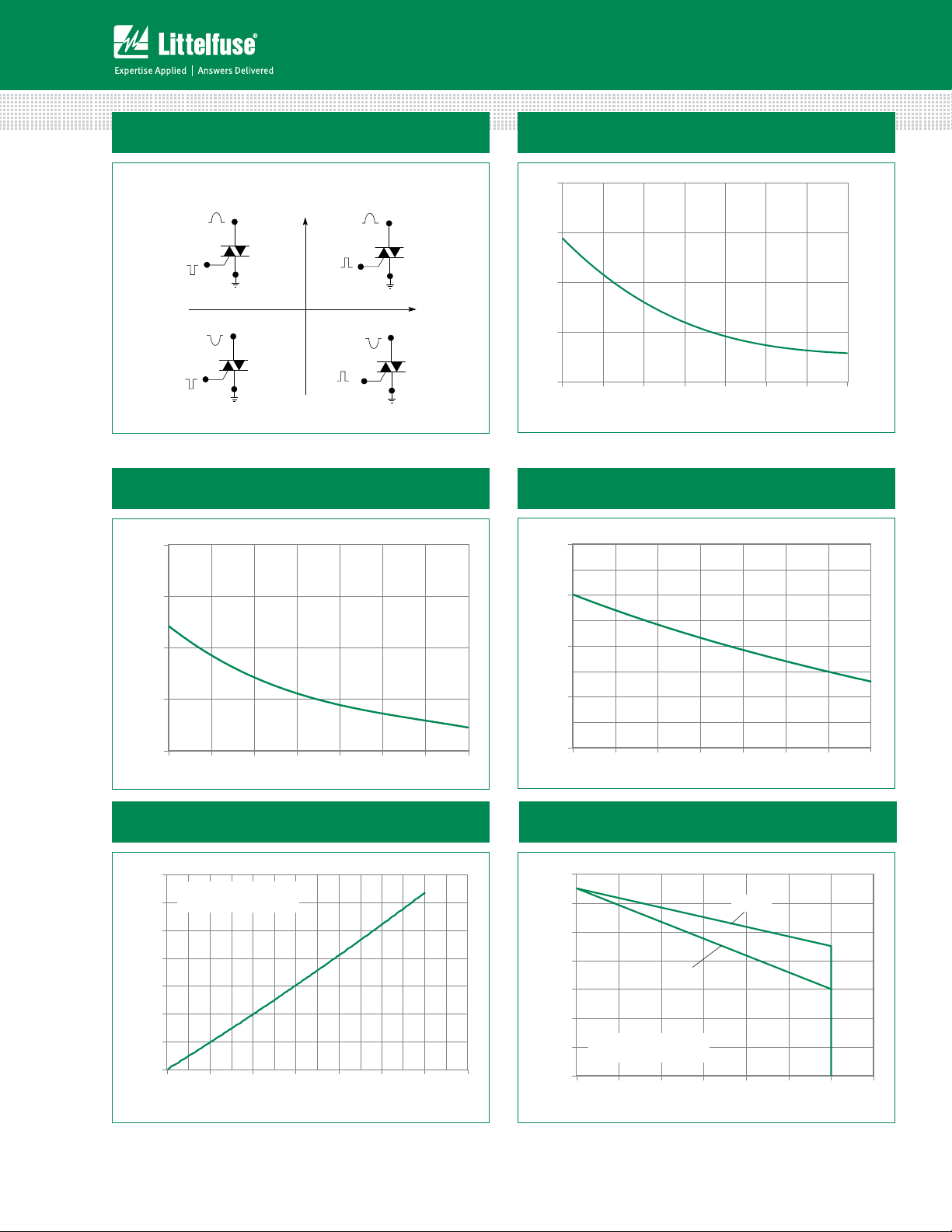
Figure 1: Definition of Quadrants
ALL POLARITIES ARE REFERENCED TO MT1
MT2 POSITIVE
(Positive Half Cycle)
(-)
I
GT
GATE
MT2
+
(+)
MT1
I
REF
-
GT
(-)
I
GT
GATE
MT2
QII
QIII
QI
QIV
(+)
MT1
REF
-
MT2 NEGATIVE
(Negative Half Cycle)
I
GT
GATE
I
GT
GATE
MT2
MT1
REF
+ I
MT2
MT1
REF
Note: Alternistors will not operate in QIV
Figure 3: Normalized DC Holding Current
vs. Junction Temperature
4.0
Figure 2: Normalized DC Gate Trigger Current for
All Quadrants vs. Junction Temperature
4.0
3.0
= 25 ºC)
J
(T
GT
/ I
2.0
GT
GT
1.0
Ratio of I
0.0
-65 -40 -15 10 35 60 85 110
Junction Temperature (TJ) - C
Figure 4: Normalized DC Gate Trigger Voltage for
All Quadrants vs. Junction Temperature
2.0
3.0
= 25ºC)
J
(T
H
2.0
/ I
H
1.0
Ratio of I
0.0
-65 -40 -15 10 35 60 85 110
Junction Temperature (TJ) - ºC
Figure 5: Power Dissipation (Typical)
vs. RMS On-State Current
14
CURRENT WAVEFORM: Sinusoidal
LOAD: Resistive or Inductive
12
CONDUCTION ANGLE: 360°
10
8
] -- Watts
6
D(AV)
[P
4
2
Average On -State P ower Dissipation
0
02468101
RMS On -Sta te Curre nt [I
T(RMS )
] -- Amps
214
1.5
= 25ºC)
J
(T
GT
1.0
/ V
GT
0.5
Ratio of V
0.0
-65 -40 -15 10 35 60 85 110
Junction Temperature (TJ) - ºC
Figure 6: Maximum Allowable Case Temperature
vs. On-State Current
130
120
110
100
) - °C
C
(T
90
80
CURRENT WAVEFORM: Sinusoidal
70
LOAD: Resistive or Inductive
Maximum Allowable Case Temperature
CONDUCTION ANGLE: 360°
60
02468101
Qxx12LH5
RMS On-State Current [I
Qxx12RH5
Qxx12NH5
T(RMS)
] - Amps
214
Qxx12xHx Series
109
Specifications are subject to change without notice.
©2013 Littelfuse, Inc
Revised: 09/23/13
 Loading...