

Page 1
LITE-ON TECHNOLOGY CORPORATION
Property of LITE-ON Only
FEATURES
* High current transfer ratio
( CTR : MIN. 600% at IF = 1mA, VCE = 2V )
* High input-output isolation voltage
( Viso = 5,000Vrms )
* Response time
( tr : TYP. 60µs at VCE = 2V, IC = 10mA, RL = 100Ω )
* Dual-in-line package :
LTV-815 : 1-channel type
LTV-825 : 2-channel type
LTV-845 : 4-channel type
* Wide lead spacing package :
LTV-815M : 1-channel type
LTV-825M : 2-channel type
LTV-845M : 4-channel type
* Surface mounting package :
LTV-815S : 1-channel type
LTV-825S : 2-channel type
LTV-845S : 4-channel type
* Tape and reel packaging :
LTV-815S-TA1, LTV-825S-TA1
* UL approved ( No. E113898 )
* TUV approved ( No. R9653630 )
* CSA approved ( No. CA91533-1 )
* FIMKO approved ( No. 193422-01 )
* NEMKO approved ( No. P96103013 )
* DEMKO approved ( No. 303986 )
* SEMKO approved ( No. 9646047 / 01-30 )
* VDE approved ( No. 094722 )
Part No. : LTV-815 / 825 / 845 ( M, S, S-TA1 ) Page : 1 of 12
BNS-OD-C131/A4
Page 2
LITE-ON TECHNOLOGY CORPORATION
Property of LITE-ON Only
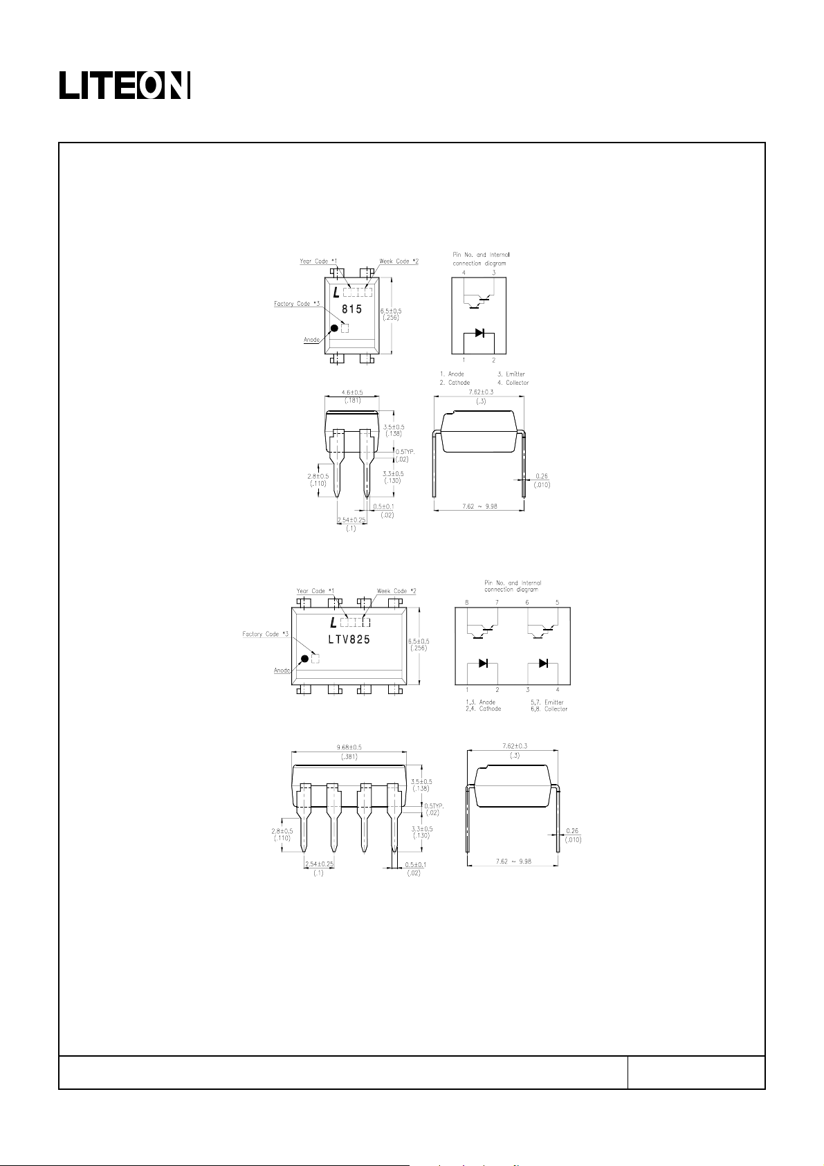
OUTLINE DIMENSIONS
LTV-815 :
LTV-825 :
*1. Year date code.
*2. 2-digit work week.
*3. Factory identification mark shall be marked (Z : Taiwan, Y : Thailand, X : China).
Part No. :
BNS-OD-C131/A4
LTV-815 / 825 / 845 ( M, S, S-TA1 )
Page :
2 of 12
Page 3
LITE-ON TECHNOLOGY CORPORATION
Property of LITE-ON Only
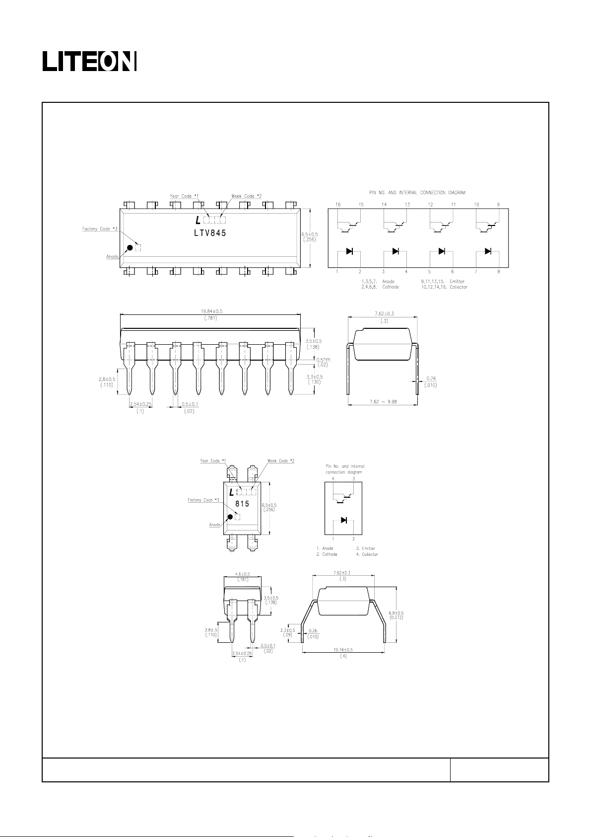
OUTLINE DIMENSIONS
LTV-845 :
LTV-815M :
*1. Year date code.
*2. 2-digit work week.
*3. Factory identification mark shall be marked (Z : Taiwan, Y : Thailand, X : China).
Part No. :
BNS-OD-C131/A4
LTV-815 / 825 / 845 ( M, S, S-TA1 )
Page :
3 of 12
Page 4
LITE-ON TECHNOLOGY CORPORATION
Property of LITE-ON Only
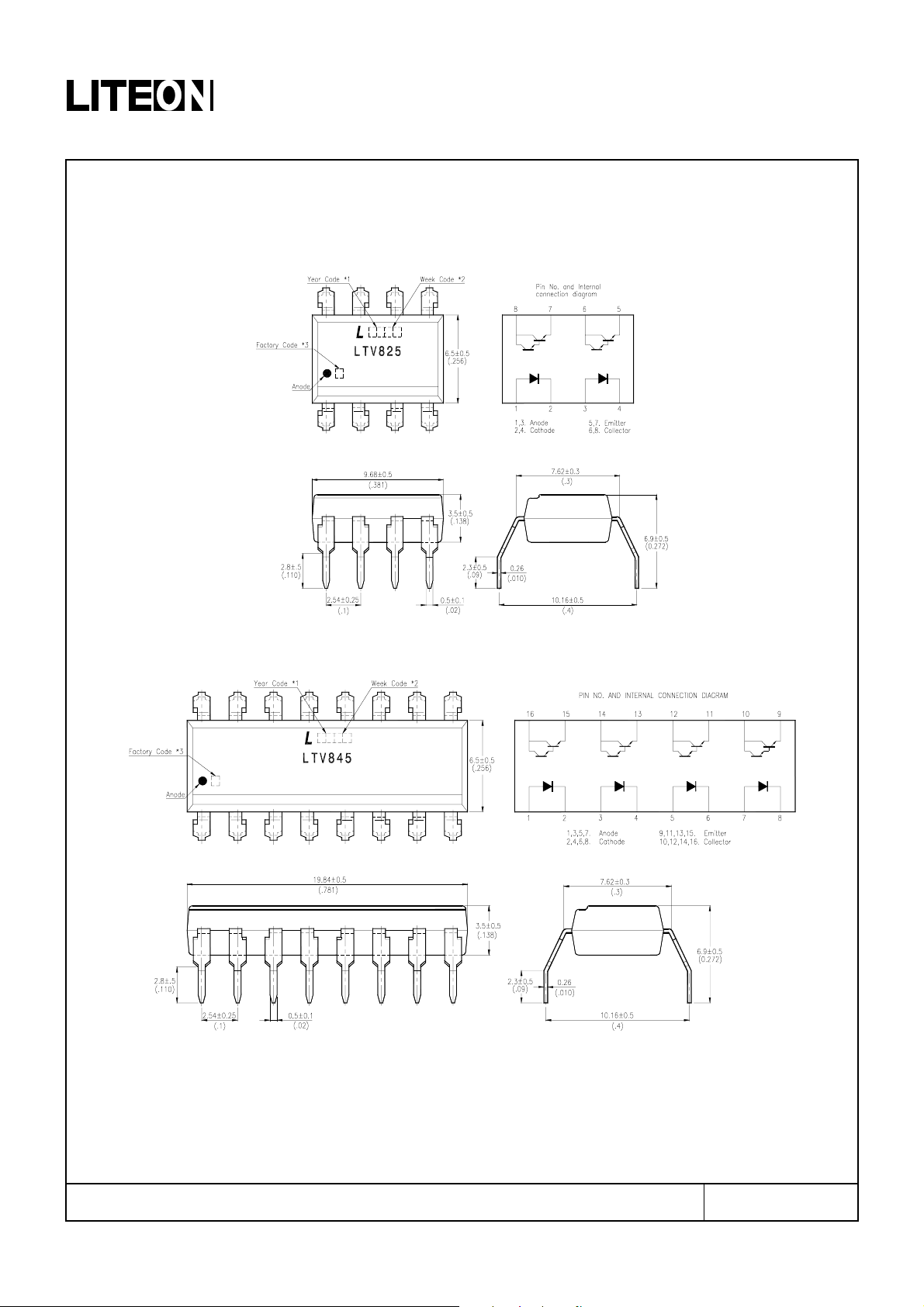
OUTLINE DIMENSIONS
LTV-825M :
LTV-845M :
*1. Year date code.
*2. 2-digit work week.
*3. Factory identification mark shall be marked (Z : Taiwan, Y : Thailand, X : China).
Part No. :
BNS-OD-C131/A4
LTV-815 / 825 / 845 ( M, S, S-TA1 )
Page :
4 of 12
Page 5

LITE-ON TECHNOLOGY CORPORATION
Property of LITE-ON Only
OUTLINE DIMENSIONS
LTV-815S :
LTV-825S :
*1. Year date code.
*2. 2-digit work week.
*3. Factory identification mark shall be marked (Z : Taiwan, Y : Thailand, X : China).
Part No. :
BNS-OD-C131/A4
LTV-815 / 825 / 845 ( M, S, S-TA1 )
Page :
5 of 12
Page 6

LITE-ON TECHNOLOGY CORPORATION
Property of LITE-ON Only
OUTLINE DIMENSIONS
LTV-845S :
*1. Year date code.
*2. 2-digit work week.
*3. Factory identification mark shall be marked (Z : Taiwan, Y : Thailand, X : China).
Part No. :
BNS-OD-C131/A4
LTV-815 / 825 / 845 ( M, S, S-TA1 )
Page :
6 of 12
Page 7

LITE-ON TECHNOLOGY CORPORATION
Property of LITE-ON Only
TAPING DIMENSIONS
LTV-815S-TA1 :
LTV-825S-TA1 :
Description Symbol Dimensions in mm ( inches )
Tape wide W
Pitch of sprocket holes P
Distance of compartment
Distance of compartment to compartment P
F
P
16 ± 0.3 ( .63 )
0
2
1
4 ± 0.1 ( .15 )
7.5 ± 0.1 ( .295 )
2 ± 0.1 ( .079 )
12 ± 0.1 ( .472 )
Part No. :
LTV-815 / 825 / 845 ( M, S, S-TA1 )
BNS-OD-C131/A4
Page :
7 of 12
Page 8

LITE-ON TECHNOLOGY CORPORATION
Property of LITE-ON Only
ABSOLUTE MAXIMUM RATING
INPUT
OUTPUT
Total Power Dissipation Ptot 200 mW
*1 Isolation Voltage Viso 5,000 Vrms
Operating Temperature Topr -30 ~ +100
Storage Temperature Tstg -55 ~ +125
PARAMETER SYMBOL RATING UNIT
Forward Current IF 50 mA
Reverse Voltage VR 6 V
Power Dissipation P 70 mW
Collector - Emitter Voltage VCEO 35 V
Emitter - Collector Voltage VECO 6 V
Collector Current IC 80 mA
Collector Power Dissipation P
C 150 mW
( Ta = 25°C )
°C
°C
*2 Soldering Temperature T
*1. AC For 1 Minute, R.H. = 40 ~ 60%
Isolation voltage shall be measured using the following method.
(1) Short between anode and cathode on the primary side and between collector and
emitter on the secondary side.
(2) The isolation voltage tester with zero-cross circuit shall be used.
(3) The waveform of applied voltage shall be a sine wave.
*2. For 10 Seconds
Part No. :
LTV-815 / 825 / 845 ( M, S, S-TA1 )
sol 260
Page :
°C
8 of 12
BNS-OD-C131/A4
Page 9

LITE-ON TECHNOLOGY CORPORATION
Property of LITE-ON Only
ELECTRICAL - OPTICAL CHARACTERISTICS
PARAMETER SYMBOL MIN. TYP. MAX. UNIT CONDITIONS
( Ta = 25°C )
Forward Voltage VF — 1.2 1.4 V IF=20mA
INPUT
OUTPUT
Reverse Current IR — — 10
Terminal Capacitance C
t — 30 250 pF V=0, f=1KHz
Collector Dark Current ICEO — — 1
Collector-Emitter
Breakdown Voltage
Emitter-Collector
Breakdown Voltage
BV
CEO 35 — — V
BV
ECO 6 — — V
Collector Current IC 6 — 75 mA
* Current Transfer Ratio CTR 600 — 7,500 %
Collector-Emitter
Saturation Voltage
V
CE(sat) — 0.8 1 V
VR=4V
µA
VCE=10V, IF=0
µA
I
I
I
I
I
V
I
I
C=0.1mA
F=0
E=10µA
F=0
F=1mA
CE=2V
F=20mA
C=5mA
TRANSFER
CHARACTERISTICS
I
*
CTR
C
=×
100%
I
F
Isolation Resistance Riso
5×10101×10
11
—
DC500V
Ω
40 ~ 60% R.H.
Floating Capacitance Cf — 0.6 1 pF V=0, f=1MHz
CE=5V, IC=2mA
Cut-Off Frequency fc 1 6 — kHz
Response Time (Rise) tr — 60 300
Response Time (Fall) t
f — 53 250
V
L=100Ω, -3dB
R
µs
V
CE=2V, IC=10mA
RL=100Ω
µs
Part No. :
LTV-815 / 825 / 845 ( M, S, S-TA1 )
BNS-OD-C131/A4
Page :
9 of 12
Page 10

LITE-ON TECHNOLOGY CORPORATION
Property of LITE-ON Only
CHARACTERISTICS CURVES
Fig.1 Forward Current vs. Ambient Fig.2 Collector Power Dissi pation vs.
Temperature
60
50
)
A
m
(
40
F
I
t
n
e
r
r
30
u
c
d
r
20
a
w
r
o
F
10
0
0 25 50 75 100 125
-30
Ambient temperature Ta ( C) Ambient temperature Ta ( C)
O
Ambient Temperature
200
)
W
m
(
c
P
150
n
o
i
t
a
p
i
s
s
i
100
d
r
e
w
o
p
r
50
o
t
c
e
l
l
o
C
-3000 12525 50 75 100
O
Fig.3 Collector-emitter Saturation
Voltage vs. Forward Current
8
e
g
a
7
t
l
o
v
6
n
o
i
t
a
r
5
u
t
a
s
4
r
e
t
t
i
3
m
e
-
r
)
2
t
o
t
a
c
s
e
(
l
l
1
E
o
C
V
C
0
0 0.5 1.0 1.5 2.0 2.5 4.03.0 3.5
A
A
A
m
0
m
m
3
5
7
A
A
m
m
1
3
A
m
5
.
0
=
c
I
A
m
0
5
F
Ta= 25 C
o
Fig.5 Current Transfer Ratio vs. Forward
Current
2000
)
%
(
1600
R
T
C
o
i
t
1200
a
r
r
e
f
s
n
800
a
r
t
t
n
e
r
r
400
u
C
0
0.1 0.2 0.5 1 2 5 10
Forward current I (mA) Collector-emitter voltage V (V)
V = 2V
Ta= 25 C
F
CE
o
Fig.4 Forward Current vs. Forward
Voltage
500
200
)
A
m
100
(
F
I
t
50
n
e
r
r
u
20
c
d
r
10
a
w
r
5
o
F
2
010.5 1.0 3.01.5 2.0 2.5
Ta= 75 C
50 C
Forward voltage V (V)Forward current I (mA)
o
o
-25 C
F
Fig.6 Collector Current vs.
Collector-emitter Voltage
100
)
80
A
m
(
c
I
t
n
e
r
r
u
c
r
o
t
c
e
l
l
o
C
I = 10mA
F
60
5mA
40
20
0
0
12345
Ta= 25 C
Pc(MAX.)
2mA
25 C
0 C
CE
o
o
o
1mA
o
Part No. :
LTV-815 / 825 / 845 ( M, S, S-TA1 )
BNS-OD-C131/A4
Page :
10 of 12
Page 11

LITE-ON TECHNOLOGY CORPORATION
Property of LITE-ON Only
CHARACTERISTICS CURVES
Fig.7 Relative Current Transfer Ratio
vs. Ambient Temperature
150
)
%
(
o
i
t
a
r
r
e
100
f
s
n
a
r
t
t
n
e
r
r
u
50
c
e
v
i
t
a
l
e
R
0
-30
0 255075100
Ambient temperature Ta ( C) Ambient temperature Ta ( C)
F=1mA
I
V
CE=2V
o o
Fig.9 Collector Dark Current vs.
Ambient Temperature
-5
10
V = 10V
)
A
(
O
E
C
I
t
n
e
r
r
u
c
k
r
a
d
r
t
o
c
e
l
l
o
C
CE
-6
10
-7
10
-8
10
-9
10
-10
10
-11
10
-25
Ambient temperature Ta ( C)
o
Fig.8 Collector-emitter Saturation Voltage
vs. Ambient Temperature
e
g
1.0
a
t
l
o
v
n
0.8
o
i
t
a
r
u
t
0.6
a
s
r
e
t
t
i
0.4
)
m
V
e
(
-
r
)
t
o
t
a
c
s
0.2
(
e
l
l
E
o
C
V
C
0
-20
0 20406080100
I
F=20mA
I
C=5mA
Fig.10 Response Time vs. Load
Resistance
500
V
CE=2V
C=10mA
I
200
Ta=25 C
100
)
s
50
(
e
20
m
i
t
10
e
s
n
5
o
p
s
2
e
R
1
0.5
0.2
0.1 0.2 0.5 1 2 5 10
0.050 255075100
Load resistance RL(k )
tr
o
td
tf
ts
Fig.11 Frequency Response
)
B
d
(
v
A
n
i
a
g
e
g
a
t
l
o
V
Part No. :
LTV-815 / 825 / 845 ( M, S, S-TA1 )
BNS-OD-C131/A4
-10
-20
0
0.02
0.1 10 1001
Frequency f (kHz)
1k
V
CE=2V
IC= 2mA
Ta= 25 C
100
Test Circuit for Response Time
Output
Input
Output
td
tr tf
10%
90%
ts
Vcc
R
o
Input
RD
L
Test Circuit for Frequency Response
Vcc
RD
RL
Output
Page :
11 of 12
Page 12

LITE-ON TECHNOLOGY CORPORATION
Property of LITE-ON Only
RECOMMENDED FOOT PRINT PATTERNS (MOUNT PAD)
Unit : mm
4 PIN 8 PIN
16 PIN
Part No. :
BNS-OD-C131/A4
LTV-815 / 825 / 845 ( M, S, S-TA1 )
Page :
12 of 12
 Loading...