

LITEON GBU808, GBU806, GBU804, GBU802, GBU801 Datasheet
...
LITE-ON
SEMICONDUCTOR
GBU8005 thru GBU810
GLASS PASSIVA T ED BRIDGE RECTIFIERS
FEATURES
Rating to 1000V PRV
Ideal for printed circuit board
Reliable low cost construction utilizing molded plastic
technique
The plastic material has UL flamma b ility classification
94V-0
UL Recognition File # E95060
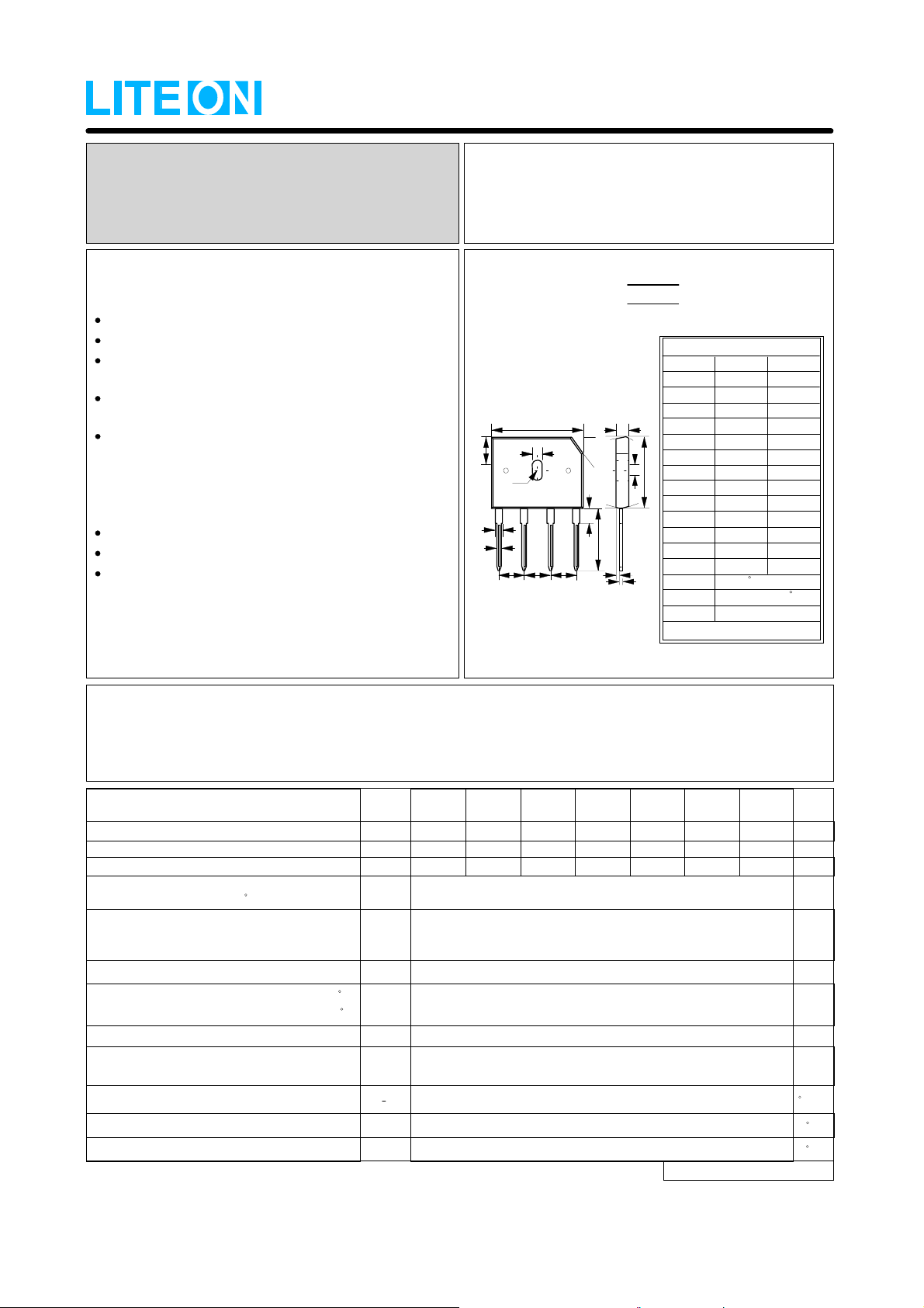
MECHANI CAL DATA
Polarity : Symbols molded on body
Weight : 0.15 ounces, 4.0 grams
Mounting position : Any
REVERSE VOLTAGE
FORWARD CURRENT
GBU
A
G
H
P
----
K
L
~~~~
~~~~
M
C
N
N
O
B
J
++++
I
NN
D
E
F
- 50 to 1000
- 8.0
Amperes
DIM.
All Dimensions in millimeter
MIN.
A
21.80
B
C
D
17.50
E
F
G
H
I
J
K
L
M
N
O
P
Volts
GBU
MAX.
22.30
18.8018.30
3.30
0.76 1.00
0.46 0.56
7.40
3.50
1.65
2.25 2.75
1.02 1.27
4.83
7.0 TYPICAL
1.90 RADIUS
3.56
18.00
7.90
4.10
2.16
2.351.95
5.33
3.2 x 45
MAXIMUM RATINGS AND ELECTRICAL CHA RACTERISTICS
Ratings at 25℃ ambient temperature unless otherwise specified.
Single phase, half wave, 60Hz, resistive or inductive load.
For capacitive load, der a te current by 2 0%
GBU
801
100
70
100
GBU
802
200
140
200
RRM
RMS
DC
F
R
I
2
J
C
0JC
J
T
STG
GBU
8005
50
35
50
CHARACTERISTICS
Maximum Recurren t Peak Reverse Voltage
Maximum RMS Voltage
Maximum DC Blocking Voltage
Maximum Average Forward
Rectif ied Current
Peak Forward Surge Current
8.3ms single half sine-wave
superimposed on rated load (JEDEC METHOD)
Maximum forward Voltage at 4.0A DC
Maximum DC Reverse Current
at Rated DC Blocking Voltage
2
I t Rating for fusing (t < 8.3ms)
Typical Junction
Capacitance per element (Note 1)
Typical Thermal Resistance (Note 2)
Operating Temperature Range
Storage Temperature Range
@TC=100 C
(with heat sink
(without heatsink )
Note 2
@TJ =25 C
@TJ =125 C
SYMBOL
V
V
V
)
(AV)
I
FSM
I
V
I t
R
T
NOTES : 1.Measured at 1.0MHz and applied reverse voltage of 4.0V DC.
2.Device mounted on 100mm x 100mm x 1.6mm Cu Plate Heatsink.
GBU
804
400
280
400
GBU
806
600
420
600
GBU
808
800
560
800
GBU
810
1000
700
1000
UNIT
8.0
3.2
200
1.0
5.0
500
166
60
2.2
A S
pF
C/W
-55 to +150
-55 to +150 C
REV. 2, 01-Dec-2000, KBDJ03
V
V
V
A
A
V
uA
2
C
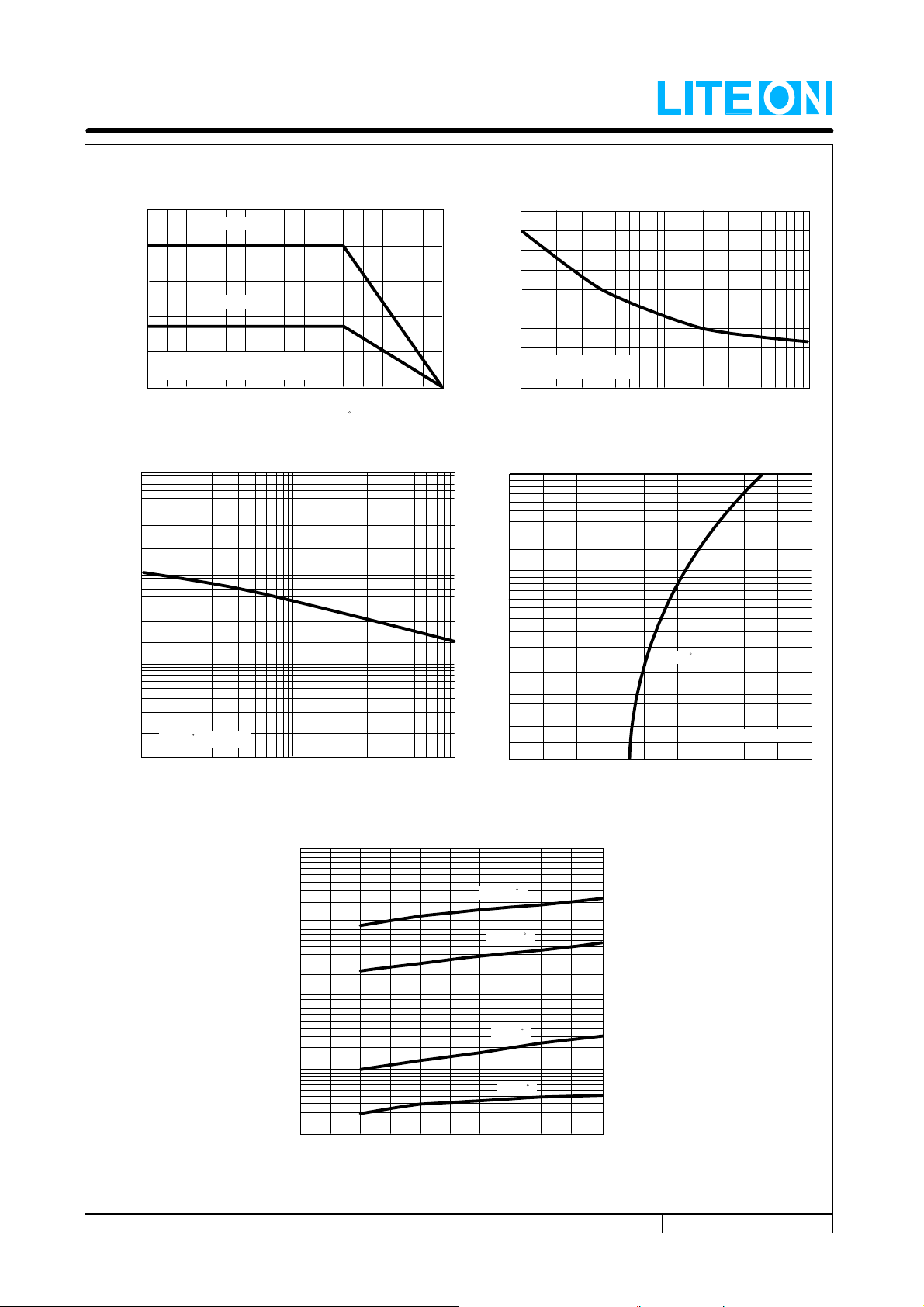
RATING AND CHARACTERISTIC CURVES
GBU8 00 5 thru GBU81 0
FIG.1 - FORWARD CURRENT DERATING CURVE
10.0
8.0
6.0
4.0
2.0
AVERAGE FORWARD CURRENT
AMPERES
0
0
1000
100
WITH HEATSINK
WITHOUT HEATSINK
SINGLE PHASE HALF WAVE 60Hz
RESISTIVE OR INDUCTIVE LOAD
40 60 100 120
20
80
CASE TEMPERATURE , C
FIG.3 - TYPICAL JUNCTION CAPACITANCE
140
FIG.2 - MAXIMUM NON-REPETITIVE SURGE CURRENT
200
150
100
50
Single Half-Sine-Wave
(JEDEC METHOD)
0
PEAK FORWARD SURGE CURRENT,
AMPERES
1 5 10 50 1002
20
NUMBER OF CYCLES A T 60Hz
FIG.4 - TYPICAL FORWARD CHARACTERISTICS
100
10
CAPACITANCE , ( p F)
10
TJ= 25 C, f = 1MHz
1
1.0
4
10
REVERS E VOLTAGE , VOLTS
100
1.0
INSTANTANEOUS FORWARD CURRENT ,(A)
0.1
0.4
0.2
0
0.6 0.8 1.0
INSTANTANEOUS FORWARD VOLTAGE , VOLTS
TJ= 25 C
PULSE WIDTH 300us
1.6
1.4
1.2
1.8
FIG.5 - TYPICAL REVERSE CHARACTERISTICS
1000
TJ= 125 C
100
10
REVERSE CURRENT ,(uA)
1.0
INSTANTANEOUS
0.1
0
20
40
PERCENT OF RATED PEAK REVERSE VOLTAGE, (%)
TJ= 100 C
TJ= 50 C
TJ= 25 C
60 80 100
REV. 2, 01-Dec-2000, KBDJ03
 Loading...