

Page 1

Service Manual
17-inch LCD Monitor
B17AAU/B17ANU/B17AAY
Page 2

Service Manual Versions and Revision
No. Version Release Date Revision
1. 1.0 Feb. 5, 2002 Original release
Copyright
Copyright 2002 LiteOn Technology Corp.
All Rights Reserved
This manual may not, in whole or in part, be copied,
photocopied, reproduced, translated, or converted to
any electronic or machine readable form without
prior written permission of LiteOn Technology
Corp.
B17AAU / B17ANU / B17AAY Service Manual.
Printed in Taiwan.
Trademarks
LiteOn is a registered trademark of LiteOn
Technology Corp.
All other trademarks are the property of their
respective owners.
Page 3

B17AAU / B17ANU / B17AAY
Table of Contents
1. Audio circuit --------------------------------------------------------------------------------------------------------------- 1
1.1 Audio input ------------------------------------------------------------------------------------------------------------ 1
1.2 Audio output ---------------------------------------------------------------------------------------------------------- 1
2. Power supply -------------------------------------------------------------------------------------------------------------- 1
3. Video input circuit -------------------------------------------------------------------------------------------------------- 1
4. Definition converter LSI peripheral circuit ---------------------------------------------------------------------------- 1
5. System reset, LED control circuit --------------------------------------------------------------------------------------- 1
6. E2PROM for PNP --------------------------------------------------------------------------------------------------------- 1
7. E2PROM -------------------------------------------------------------------------------------------------------------------- 2
8. CPU circuit ----------------------------------------------------------------------------------------------------------------- 2
8.1 Dection of POWER switch status ---------------------------------------------------------------------------------- 2
8.2 Display mode identification ----------------------------------------------------------------------------------------- 2
8.3 User control ----------------------------------------------------------------------------------------------------------- 4
8.4 Control of identification converter LSI (IC 14) ------------------------------------------------------------------ 5
8.5 I2C bus control -------------------------------------------------------------------------------------------------------- 5
8.6 Power ON sequence -------------------------------------------------------------------------------------------------- 6
8.7 Power OFF sequence ------------------------------------------------------------------------------------------------- 7
8.8 List of CPU assignments --------------------------------------------------------------------------------------------- 8
9 Power Board Operation Therory ------------------------------------------------------------------------------------------- 8
Circuit Description Index
Page 4

B17AAU / B17ANU / B17AAY
1. Audio circuit (Circuit diagrams Main PWB) KT
1.1 Audio input
The audio signal input received from the audio input terminal (P311) is applied to the amplifier I332 of 4 (L-CH)
and 9 (R-CH) through the low-pass filter consisting of R408, R410, R409, R407, C598 and C599.
In this amplifier, controls of Volume, and mute are conducted. The audio signal controlled at the pin 6 deter-
mines the attenuation of output of the amplifiers. Since then, the signal is output to the jack P312.
1.2 Audio output
The audio signal is output from the jack output terminal (P312) of the jack board to the internal speaker system.
2. Power supply (Circuit daigrams MAIN PWB 6/8, 7/8)
2.1 P310 connector
A 5V power supply for LCD module, CPU, and logic is generated from the P310 connector.
2.2 I323:3-terminal regulator
A 3.3V power supply for Scaler IC I315, LVDS IC I319, I320 is generated from the 5V source.
2.3 I324:3-terminal regulator
A 2.5V power supply for Scaler IC I315 is generated from the 5V source.
Q307, I321 ON/OFF control for LCD Module
ON/OFF control is performed for power ON/OFF and also for the power saving sequence.
3. Video input circuit (Circuit diagram MAIN PWB 3/8)
The analog video signal input entered from P304, the AC-coupled video signal is used to clamp the black level at
0V).
4. Definition converter LSI peripheral circuit (Circuit diagram MAIN PWB)
I315 gm5020 is the definition converter LSI.
The analog R, G, B signal input entered from the video input circuit is converted into the digital data of video
signal through the incorporated A/D converter. Based on this conversion, this device performs interpolation
during pixel extension. The source voltage for this device is 3.3V, 2.5V and the system clock frequency is
24MHz. The withstand voltage level for the input signal voltage if I315 is 3.3V and 5V.
5. System reset, LED control circuit (Circuit diagram MAIN PWB 2/8)
5.1 System reset
System reset is performed by detecting the rising and falling of the 5V source voltage at I301.
5.2 LED control circuit
Green / amber is lit with the control signal of the LED GREEN and LED AMBER signal pin 25, 26 from I302
(Circuit diagram MAIN PWB 2/8).
6. E2PROM for PnP (Circuit diagram MAIN PWB 3/8)
Page 1Circuit Description
Page 5

B17AAU / B17ANU / B17AAY
7. E2PROM (Circuit diagram MAIN PWB 2/8)
Data transfer between I305 (24LC16) and CPU (Circuit diagram MAIN PWB 2/8 (I302) is effected through the
IIC bus SCL (pin 17) and SDA (pin 16) of I302. The data to be transferred to each device are stored in I305.
l I315 control data.
l OSD related setting data.
l Other control data for service menu.
8. CPU circuit (Circuit diagram MAIN PWB 2/8)
I302 (87C51RD2) functions as the CPU.
The source voltage for the device is 5.0V and the system clock frequency is 24MHz.
8.1 Detection of POWER switch status
The CPU identifies the ON status of the two power supplies. The identification is made when the power supply
is turned off. For example, if the power supply is turned off with the POWER switch, the POWER switch must be
turned on when activating the power supply again. If the power supply is turned off by pulling out the power
cord, then this power supply can be turned on by connecting the power cord, without pressing the POWER
switch.
8.2 Display mode identification
8.2.1 Functions
(1) Display mode identification
l The display mode of input signal is identified based on Table 1.
l When the mode has been identified through the measurement of horizontal and vertical frequencies, the total
number of lines is determined with a formula of Horizontal frequency / Vertical frequency = Total number
of lines. Final identification can be made by examining the coincidence of the obtained figure with the
number of lines for the mode identified from the frequency. The boundary number of lines in each mode is
shown in Table 2.
l When the detected frequency if the sync signal has changed, the total number of lines should be counted even
through it is rge identified frequency in the same mode.
(2) Power save mode.
This power save mode is assumed when the frequency of the horizontal / vertical signal is as specified below.
l Vertical frequency : 50 ~ 86 Hz
l Horizontal frequency : 24 ~ 92 KHz
l VTOTAL : 1200 or more.
(3) Power save mode.
The power save mode is assumed when the horizontal / vertical signals are as specified below.
l If there is no horizontal sync signal input.
l If there is no vertical sync signal input.
l If the horizontal sync signal is outside the measuring range of gm5020.
l If the vertical sync signal is outside the measuring range of gm5020.
Page 2 Circuit Description
Page 6

Table 1
q
(
)
B17AAU / B17ANU / B17AAY
Band Width
KHz
1. VGA 720 x 400 70Hz 31.47 28.322 - +
2. VGA 640 x 480 60Hz 31.47 25.175 - -
3. MAC 640 x 480 66Hz 35 32.24 - -
4. VESA 640 X 480 72Hz 37.86 31.5 - -
5. VESA 640 X 480 75Hz 37.5 31.5 - -
6. VESA 800 x 600 56Hz 35.16 36 + +
7. VESA 800 x 600 60Hz 37.88 40 + +
8. VESA 800 x 600 75Hz 46.88 49.5 + +
9. VESA 800 x 600 72Hz 48.08 50 + +
10. MAC 832 x 624 75Hz 49.72 57.283 - -
11. VESA 1024 x 768 60Hz 48.36 65 - -
12. VESA 1024 x 768 70Hz 56.48 75 - -
13. VESA 1024 x 768 75Hz 60.02 78.75 + +
(MHz)
PolarityMode Resolution H-fre
HV
14. VESA 1280 x 1024 60Hz 64 108 + +
15. VESA 1280 x 1024 75Hz 80 135 + +
16. VESA 1152 x 864 75Hz 67.5 108 + +
17. VESA 1280 x 960 60Hz 60 108 + +
Page 3Circuit Description
Page 7

Table 2 the number of the lines, Vsync distinction
B17AAU / B17ANU / B17AAY
Indication resolution The number of the
distinction lines
640 x 480 487 < LINE < 607 fV < 63 Hz 2
800 x 600 607 < LINE < 777 fV < 58 Hz 6
832 x 624 640 < LINE -10
1024 x 768 768 < LINE < 870 fV < 63 Hz 11
1152 x 864 870 < LINE < 1031 16
1280 x 960 960 < LINE < 1027 17
1280 x 1024 1027 < LINE 14,15
8.3 User Control
8.3.1 Related ports of I315 and pin of I302
Distinction Vsync The fixed mode
63 Hz < fV < 68 Hz 3
68 Hz < fV < 74 Hz 4
74 Hz < fV < 78 Hz 5
58 Hz < fV < 63 Hz 7
63 Hz < fV < 73 Hz 9
73 Hz < fV < 78 Hz 8
68 Hz < fV < 73 Hz 12
73 Hz < fV < 78 Hz 13
Port Pin No. I/O Signal name Function Remarks
GPI04 I315, M1 1 MENU EXIT/ENTER switch input ENTER/Withdraw
from OSD
GPI05 I315, L1 1 DOWN switch input ( ) key
GPI06 I315, G18 1 - switch input ( ) key
GPI07 I315, G19 1 + switch input ( ) key
GPI0 I302, 15 1 POWER soft power switch input ( power ) key
8.3.2 Functions
Control is effected for the push-switches to be used when the user changes the parameters, in order to modify the
respective setting values. Whether the switch has been pressed is identified with the switch input level that is
turned L.
Each switch input port is pulled up at outside of ASIC
Each parameter is stored in the EEPROM, the contents of which are updated as required.
.
Page 4 Circuit Description
Page 8

8.4 Control of definition converter LSI I315
,
8.4.1 Ports related to control
Pin No. I/O Signal name Function
R3 I IRQ gmZan1 interrupt signal
P1 O HCLK gmZan1 serial clock
P3, P4,
R2
R1
P2 O HFS gmZan1 serial select
8.4.2 Functions
Major function of I315 are as follows:
(1) Expansion of the display screen.
(2) Timing control for various signal types.
(3) Power-supply sequence (LCD panel).
8.5 I2C bus control
8.5.1 Related ports of I302
Port Pin No. I/O Signal name Function
P3.5 17 I IICCLK IIC bus clock
P3.4 16 I/O IICDATA IIC bus data
I/O HDATA gmZan1 serial data
B17AAU / B17ANU / B17AAY
8.5.2 I2C-controlled functions
The following functional controls are effected by I2C.
(1) Control of EEPROM I305f for parameter setting.
(2) Control of audio preamplifier.
Page 5Circuit Description
Page 9

B17AAU / B17ANU / B17AAY
8.6 Power ON sequence
When the POWER switch is pressed, the POWER OFF signal is turned H. When this H potential is detected,
the CPU begins to establish the respective power supplies according to the sequence shown below.
POWER
LED
LVCC
(Audio_EN)
Panel_VCC
PCLK/DATA
Backlight_EN
Page 6 Circuit Description
Page 10

B17AAU / B17ANU / B17AAY
8.7 Power OFF sequence
When the POWER switch is pressed while the power supply is ON, the POWER ON signal is turned H. When
this H potential is detected, the CPU begins to turn off the respective power supplies according to the sequence
shown below.
POWER
LVCC
(Audio_EN)
LED
Panel_VCC
Backlight_EN
PCLK/DATA
Page 7Circuit Description
Page 11

B17AAU / B17ANU / B17AAY
8.8 List of CPU Pin Assignments
Port Pin No. Signal Name Initial Setting Function Remark
~
P1.0
P1.1
P1.2
P1.3
P1.4
P1.5
P1.6
P1.9
~
P3.0
~
P3.1
P3.2
P3.3
P3.4
P3.5
P3.6
P3.7
~
~
~
~
P2.0
P2.1
P2.2
P2.3
P2.4
P2.5
P2.6
P2.7
~
~
~
~
P0.7
P0.6
P0.5
P0.4
P0.3
P0.2
P0.1
P0.0
~
!
"
#
$
%
&
'
!
"
#
$
%
&
'
!
!
!
!!
!"
!#
!$
!%
!&
!'
"
"
"
"!
""
!
"
#
$
%
&
'
NC ~ ~
HDATA0 ~ gm5020 4bit interface data
HDATA1 ~ gm5020 4bit interface data
HDATA2 ~ gm5020 4bit interface data
HDATA3 ~ gm5020 4bit interface data
HCLK ~ gm5020 4bit interface Clock
HFS ~ gm5020 data Enable
Pand-EN H Panel VCC Enable
IIC-EN H IIC Enable
RST L Reset CPU Active H
RXD H Receive data
NC ~ ~
TXD H Transmit data
IRQ ~ gm5020 interrupt signal
PWR_SW ~ ON/OFF monitor power
SDA H IIC Bus Data
SCL ~ IIC Bus Data Active L
NC ~ ~
DDC_GND L Detect Dsub cable plug-in
XTAL2 ~ Crystal signal out
XTAL ~ Crystal signal in
GND ~ ~
NC ~ ~
NC ~ ~
LED GRN H LED Green ON / OFF
LED AMB H LED Amber ON / OFF
MUTE H Audio MUTE
CUSP H Audio SUSP
BACK_EN H Backlight Enable
LVDS_ON H LVDS IC ON / OFF
NC ~ ~
PSEN# H Program store enable
NC ~ ~
NC ~ ~
EA# H External Access Enable
NC ~ ~
NC ~ ~
NC ~ ~
NC ~ ~
NC ~ ~
NC ~ ~
NC ~ ~
NC ~ ~
VCC ~ VCC
Page 8 Circuit Description
Page 12

B17AAU / B17ANU / B17AAY
9. Power Board Operation Therory
9.1 Line filter consists of C801, T801, C802, C803, C804. It eliminates high frequency interference to meet EMIs
requirement.
9.2 Rec & Filter
Bridge diode D801 converts AC source into pulsed DC. This pulsed DC is smoothed and filtered by C805. R802
is an NTC ( negative thermal coefficient ) resistor, used to reduce inrush current to be within safe range.
9.3 Power transformer :
T802 converts energy for square wave from power source C805 to secondary side to generate +12V and +5V.
9.4 Output :
The square wave from T802 is rectified by D809, D810, then filtered by C817, C822 to generate +12V and +5V
respectively.
9.5 Driver :
Q803 drive T802 from PWM control of I801 for power converted.
9.6 FB :
Negative feedback CKT consists of photo coupler I802 and adjustable regulator I803. It can maintain output
voltages +5V and +12V at a stable level.
9.79.7
PWM :PWM :
9.7
PWM :
9.79.7
PWM :PWM :
9.7.19.7.1
9.7.1
9.7.19.7.1
9.7.29.7.2
9.7.2
9.7.29.7.2
9.7.39.7.3
9.7.3
9.7.39.7.3
Start : When power is turned on, Q801 conducts due to bias from C805 and R805,R803. C807 is charStart : When power is turned on, Q801 conducts due to bias from C805 and R805,R803. C807 is char
Start : When power is turned on, Q801 conducts due to bias from C805 and R805,R803. C807 is char
Start : When power is turned on, Q801 conducts due to bias from C805 and R805,R803. C807 is charStart : When power is turned on, Q801 conducts due to bias from C805 and R805,R803. C807 is char
16 volt and a starting current about 0.3mA to pin 7 of I801. I801 starts to oscillate and outputs a pulse train16 volt and a starting current about 0.3mA to pin 7 of I801. I801 starts to oscillate and outputs a pulse train
16 volt and a starting current about 0.3mA to pin 7 of I801. I801 starts to oscillate and outputs a pulse train
16 volt and a starting current about 0.3mA to pin 7 of I801. I801 starts to oscillate and outputs a pulse train16 volt and a starting current about 0.3mA to pin 7 of I801. I801 starts to oscillate and outputs a pulse train
through pin 6 to drive Q803.through pin 6 to drive Q803.
through pin 6 to drive Q803.
through pin 6 to drive Q803.through pin 6 to drive Q803.
OPP : When Q803 turns on, C805 supplies a linearly increasing triangle current through the primary induc-OPP : When Q803 turns on, C805 supplies a linearly increasing triangle current through the primary induc-
OPP : When Q803 turns on, C805 supplies a linearly increasing triangle current through the primary induc-
OPP : When Q803 turns on, C805 supplies a linearly increasing triangle current through the primary induc-OPP : When Q803 turns on, C805 supplies a linearly increasing triangle current through the primary induc-
tance of T802 to the driver Q803, once the peak value of this current multiplied by R81tance of T802 to the driver Q803, once the peak value of this current multiplied by R81
tance of T802 to the driver Q803, once the peak value of this current multiplied by R81
tance of T802 to the driver Q803, once the peak value of this current multiplied by R81tance of T802 to the driver Q803, once the peak value of this current multiplied by R81
pulse train will be turn ofpulse train will be turn of
pulse train will be turn of
pulse train will be turn ofpulse train will be turn of
Regulation : If output voltage +5V goes up, the R terminal of I803 gets more bias, accordingly photoRegulation : If output voltage +5V goes up, the R terminal of I803 gets more bias, accordingly photo
Regulation : If output voltage +5V goes up, the R terminal of I803 gets more bias, accordingly photo
Regulation : If output voltage +5V goes up, the R terminal of I803 gets more bias, accordingly photoRegulation : If output voltage +5V goes up, the R terminal of I803 gets more bias, accordingly photo
transistor and photo diode flows more current. The voltage of pin 2 goes up too, making the pulse width oftransistor and photo diode flows more current. The voltage of pin 2 goes up too, making the pulse width of
transistor and photo diode flows more current. The voltage of pin 2 goes up too, making the pulse width of
transistor and photo diode flows more current. The voltage of pin 2 goes up too, making the pulse width oftransistor and photo diode flows more current. The voltage of pin 2 goes up too, making the pulse width of
pin 6 to become narrower. So the output voltage +5V will be pulled down to a stable value.pin 6 to become narrower. So the output voltage +5V will be pulled down to a stable value.
pin 6 to become narrower. So the output voltage +5V will be pulled down to a stable value.
pin 6 to become narrower. So the output voltage +5V will be pulled down to a stable value.pin 6 to become narrower. So the output voltage +5V will be pulled down to a stable value.
f immediately to protect Q803, T802 from being burned out.f immediately to protect Q803, T802 from being burned out.
f immediately to protect Q803, T802 from being burned out.
f immediately to protect Q803, T802 from being burned out.f immediately to protect Q803, T802 from being burned out.
1 exceeds1 volt,1 exceeds1 volt,
1 exceeds1 volt,
1 exceeds1 volt,1 exceeds1 volt,
ged aged a
ged a
ged aged a
9.7.49.7.4
9.7.4
9.7.49.7.4
9.7.59.7.5
9.7.5
9.7.59.7.5
OVP : If +5V goes up too much, the induced voltage on pin 4 of T802 becomes larOVP : If +5V goes up too much, the induced voltage on pin 4 of T802 becomes lar
OVP : If +5V goes up too much, the induced voltage on pin 4 of T802 becomes lar
OVP : If +5V goes up too much, the induced voltage on pin 4 of T802 becomes larOVP : If +5V goes up too much, the induced voltage on pin 4 of T802 becomes lar
over 18 volts, ZD801 conducts, pin 3 of I801 is pulled up over 1 volt. The pulse train at pin 6 goes down toover 18 volts, ZD801 conducts, pin 3 of I801 is pulled up over 1 volt. The pulse train at pin 6 goes down to
over 18 volts, ZD801 conducts, pin 3 of I801 is pulled up over 1 volt. The pulse train at pin 6 goes down to
over 18 volts, ZD801 conducts, pin 3 of I801 is pulled up over 1 volt. The pulse train at pin 6 goes down toover 18 volts, ZD801 conducts, pin 3 of I801 is pulled up over 1 volt. The pulse train at pin 6 goes down to
zero, shutting Q803 ofzero, shutting Q803 of
zero, shutting Q803 of
zero, shutting Q803 ofzero, shutting Q803 of
SCP : If output terminal is short to ground, photo transistor does not conduct, hence Q806 does not conductSCP : If output terminal is short to ground, photo transistor does not conduct, hence Q806 does not conduct
SCP : If output terminal is short to ground, photo transistor does not conduct, hence Q806 does not conduct
SCP : If output terminal is short to ground, photo transistor does not conduct, hence Q806 does not conductSCP : If output terminal is short to ground, photo transistor does not conduct, hence Q806 does not conduct
eithereither
. Then oscillation of I801 is stop, shutting Q803 of. Then oscillation of I801 is stop, shutting Q803 of
either
. Then oscillation of I801 is stop, shutting Q803 of
eithereither
. Then oscillation of I801 is stop, shutting Q803 of. Then oscillation of I801 is stop, shutting Q803 of
f immediatelyf immediately
f immediately
f immediatelyf immediately
..
.
..
f immediatelyf immediately
f immediately
f immediatelyf immediately
..
.
..
ge also. Suppose that it isge also. Suppose that it is
ge also. Suppose that it is
ge also. Suppose that it isge also. Suppose that it is
B17AAU Power Board Block Diagram
Line
Filter
Rec. &
Filter
PWM Driver
Power
Transformer
FB
Outpur Rec. & Filter
Circuit Description Index
Page 13

B17AAU / B17ANU / B17AAY
Table of Contents
1. No display of screen (Screen is black, color of LED is amber) ----------------------------------------------------- 1
2. Nothing displays on screen (Screen is black, color of LED is green) ---------------------------------------------- 2
3. Checking the back light unit --------------------------------------------------------------------------------------------- 5
4. Abnormal screen ---------------------------------------------------------------------------------------------------------- 6
5. Abnormal Auto adjustment ---------------------------------------------------------------------------------------------- 8
5.1 NO OSM display ----------------------------------------------------------------------------------------------------- 8
5.2 OSD Adjust problem ------------------------------------------------------------------------------------------------- 8
6. Abnormal plug and play operation ------------------------------------------------------------------------------------- 9
6.1 Abnormal DDC2 ------------------------------------------------------------------------------------------------------ 9
7. Checking the interface circuit of sync signal -------------------------------------------------------------------------10
7.1 Checking the control circuit of horizontal sync pulse ---------------------------------------------------------- 10
7.2 Checking the control circuit of vertical sync pulse-------------------------------------------------------------- 10
8. Checking the resolution change IC movement -----------------------------------------------------------------------11
9. No power on -------------------------------------------------------------------------------------------------------------- 12
10. Checking the DC/DC converter circuit -------------------------------------------------------------------------------- 13
11. Checking the operation of CPU ---------------------------------------------------------------------------------------- 14
12. Power board --------------------------------------------------------------------------------------------------------------- 15
Index Trouble Shooting
Page 14

B17AAU / B17ANU / B17AAY
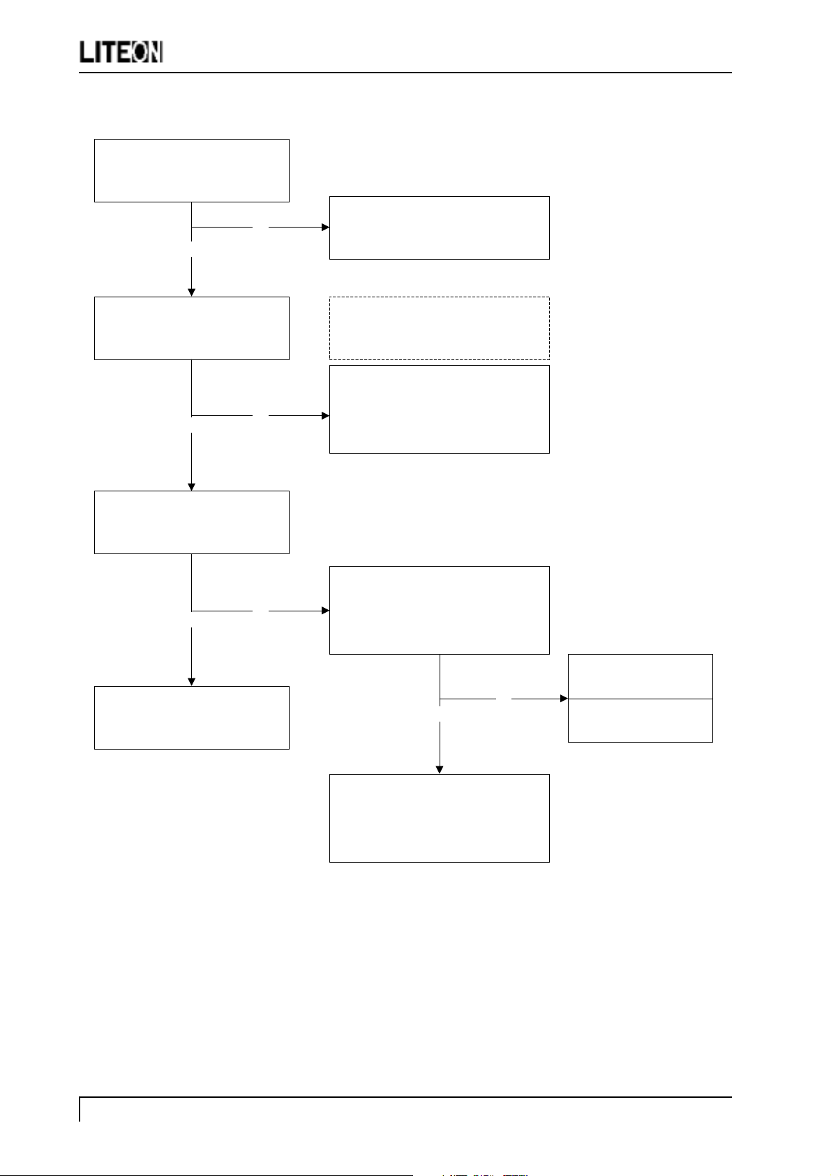
1. No display of screen (Screen is black, color of LED is amber)
Does OSM display when you push
PROCEED button.
When a signal isn't
being inputted, it is
indicated with "VIDEO
INPUT". It is indicated
with "OUT OF RANGE"
at the time of the
frequency that it can't be
distinguished.
Check if the sync signal from Computer
is output and if the video cable is
Yes
connected normally.
No
Preceed "No OSM display"section.
OK
NG
Proceed "Checking the resolution change
IC movement" section.
Input the sync signal of computer, or
change the cable.
Trouble Shooting Page 1
Page 15
B17AAU / B17ANU / B17AAY
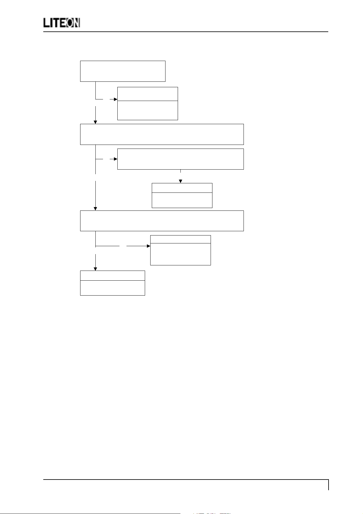
2. Nothing displays on screen (Screen is black, color of LED is green)
Is backlight lit?
NG Refer "Checking the backlight unit" section
OK
Does computer output RGB video signals?
OK
Check OSM menu is displayed on screen
when you push the "PROCEED" key.
OK
Proceed "Abnormal screen" section.
NG
NG
Check the video cable for failure. Check the host for
output signal with all black only.
1) Change pattern of video signal output on the
host.
2) Reconnect the video cable.
3) Change the video cable.
Check if the LCD video signal cable is connected
between the MAIN PWB and LCD module.
NG
OK
Failure Point
The Cable is disconnected.
Next Page
Page 2 Trouble Shooting
Page 16

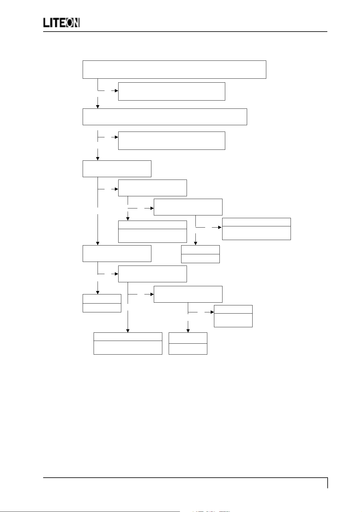
Continue
Check the 3.3 V power are supplied on I323, pin 2.
Check if the voltage on I323 pin 3 that
NG
is high level DC at 5V.
B17AAU / B17ANU / B17AAY
Failure point
OK
Failure point
I323 Failure
Is a dot clock being outputted under the
condition that a LCD module is
connected to L322 pin 2?
OK
Check the H-sync pulse of negative polarity
is output on RN314 pin 8 at TTL level.
OK
NG
NG
OK
NG
1) Printed wire broke between P310 pin 7, 8 and
and I323.
2) Check power board.
Failure point
1) I315 failure
2) Printed wire broke between I315 and L322 pin 2.
Failure point
1) I315 failure
2) Printed wire broke between I315 and RN314 pin 8.
Check the V-sync of negative polarity
are output on RN314 pin 7.
Failure point
OK
Next Page
NG
1) I315 failure
2) Printed wire broke between I315 and RN314 pin 7.
Trouble Shooting Page 3
Page 17

Continue
Check the data enable of positive polarity are output on RN314 pin 6.
OK
NG
1) I315 failure.
2) Printed wire broke between I315 and RN314 pin 6.
B17AAU / B17ANU / B17AAY
Failure point
Check the data signal output on I315 R, G, B
Check I319, I320 all LVDS signal pins.
1) The cable broke between P304 and LCD
module.
2) LCD module failure.
data pin.
OK
OK
Failure point
NG
NG
Failure point
1) I315 failure.
Failure point
1) I319, I320 failure.
2) Printed wire broke between I319, I320 and P307.
Page 4 Trouble Shooting
Page 18
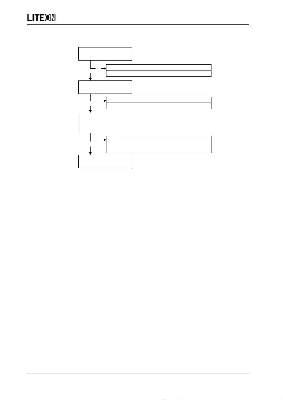
3. Checking the back light unit
Is +12V supplied to inverter PWB?
B17AAU / B17ANU / B17AAY
NG
OK
Check the BKLT_EN signal of the rectangle input P310 pin 2 at TTL high level
NG
OK
Check the PWM signal of the input from I315 pin M4 (R374 pin 2) is a PWM signal.
OK
Failure point
1) Inverter cable disconnection.
2) Power board failure.
Is a "H" level being output in the TTL level from I302 pin 29
Or, is BKLT_EN signal of the rectangle being output?
NG
Failure point
Printed wire broke between
I302 pin 29 and R326.
NG
Failure point
1) Printed wire broke between
I315 pin M4 and R374 pin 2.
2) I315 failure.
Failure point
1) Inverter cable disconnection.
2) Inverter of LCD module failure.
Trouble Shooting Page 5
Page 19

4. Abnormal screen
B17AAU / B17ANU / B17AAY
Check the R, G, B video signal from computer input on
Check the R, G, B input signals on I315 pin E1, D2, C1
Is the pulse of the TTL level being output to I319, I320
Check the negative horizontal sync pulse output to
D-Sub R, G, B connector.
OK
respectively that their level is 0.7Vp-p maximum.
OK
from the data line of I315?
OK
RN314 pin 8 from I315 pin F20 at TTL level.
NG
NG
NG
1) No R, G and B video signal output from host computer. Check
computer
2) Video signal cable disconnection.
In the case of the Red signal. (A Green and Blue signal is the same
path, too.)
1) Printed wire broke between D-Sub(R) and I315 pin E1.
2) R339 short.
3) C359 open.
4) R337 open.
1) Printed wire broke between I315 data line and I319, I320.
2) I315 failure.
Failure point
Failure point
Failure point
OK
Check the negative vertical sync pulse output to RN314
pin 7 from I315 pin F19 at TTL level.
OK
Check the positive DE pulse output to RN314 pin 6 from
I315 pin F18 at TTL level.
OK
Check the SHFCLK OUTPUT to L322 pin 2 from I315 pin
G20 at TTL level.
OK
Next Page
NG
NG
NG
NG
1) Printed wire broke between I315 pin F20 and RN314 pin 8.
2) I315 failure
1) Printed wire broke between I315 pin 73 and RN314 pin 7.
2) I315 failure
1) Printed wire broke between I315 pin F18 and RN314 pin 6.
2) I315 failure
1) Printed wire broke between I315 pin G20 and L322 pin 2.
2) L321 open
3) C583 short
4) C590 short
5) L322 short
6) I315 failure
Failure point
Failure point
Failure point
Failure point
Page 6 Trouble Shooting
Page 20

Continue
Check I319, I320 all LVDS signal pins.
OK
NG
B17AAU / B17ANU / B17AAY
Failure point
1) I319, I320 faulure.
2) Printed wire broken between I319, I320 and P307.
Process "Checking the resolution change IC movement"
section.
Trouble Shooting Page 7
Page 21

5. Abnormal OSM display
5.1 NO OSM display
Check the input of 3.3Vp-p pulse from I315 pin P3, P4, R1, R2, P2, P1.
1) Printed wire broke between I315 pin P3 and I302 pin 5.
2) Printed wire broke between I315 pin P4 and I302 pin 4.
NG
OK
3) Printed wire broke between I315 pin R1 and I302 pin 3.
4) Printed wire broke between I315 pin R2 and I302 pin 2.
5) Printed wire broke between I315 pin P2 and I302 pin 7.
6) Printed wire broke between I315 pin P1 and I302 pin 6.
7) RN301, RN303 open/short.
B17AAU / B17ANU / B17AAY
Failure point
Proceed "Checking the resolution change IC movement" section.
5.2 OSD Adjust problem
Check the input TTL level whether was changed when pressed function keys.
NG
OK
Failure point
1) Printed wire broke between P302 pin 3 and I302 pin 15.
2) Printed wire broke between P302 pin 4 and I315 pin G19.
3) Printed wire broke between P302 pin 5 and I315 pin G18.
4) Printed wire broke between P302 pin 6 and I315 pin L1.
5) Printed wire broke between P302 pin 7 and I315 pin M1.
6) C322, C323, C324, C326, C327 short.
7) RN306, RN307, short/open.
8) I315 failure.
Proceed "Checking the resolution change IC movement" section.
Page 8 Trouble Shooting
Page 22

6. Abnormal plug and play operation
6.1 Abnormal DDC2
Confirm the output of serial data on I312 pin 6 synchronize SCLK at TTL level.
B17AAU / B17ANU / B17AAY
NG
OK
Failure point
1) The host machine isn't communicating in DDC2 mode.
2) The video cable may have failed or may not to have connections for DDC.
3) Between I312 pin 6 and P304 pin 15 may have failed.
4) R335 open.
5) Cable failure.
Failure point
I312 failure.
Trouble Shooting Page 9
Page 23

7. Checking the interface circuit of sync signal
7.1 Checking the control circuit of horizontal sync pulse
B17AAU / B17ANU / B17AAY
Check the horizontal sync signal on I315
Process "Checking the resolution change IC
pin L2 TTL level.
NG
OK
movement" section.
1) Video cable may have failed.
2) Printed wire broke between P304 pin 13
and I315 pin L2
3) FB305, R329 open
4) R330, C352 short
7.2 Checking the control circuit of vertical sync pulse
Check the vertical sync signal on I315 pin
K1 TTL level.
Failure point
NG
1) Video cable may have failed.
OK
Process "Checking the resolution change IC
movement" section.
2) Printed wire broke between P304 pin 14 and I315
pin K1
3) FB328, FB304 open
4) R331, C353 short
Failure point
Page 10 Trouble Shooting
Page 24
8. Checking the resolution change IC movement
Is there +3.3V supply on I315 pin D13, D15, D16, E17, G17, J17, L17, N17, R17, U17, U15, U13,
U12, U10, U8, U6, U5, T4, L4, B2, B6, B7, B8, B9, B11, C3, D3, E3, F2, F4, G1, G3, H1, J1, J3.
NG
OK
Proceed "Checking the DC/DC converter circuit" section.
B17AAU / B17ANU / B17AAY
Is there +2.5V supply on I315 pin D12, D14, D17, F17, K17, M17, P17, T17, U16, U14,
OK
Is 24MHz clock input to I315 pin J4
OK
Is +5.0V supplied to I315 pin T1 at
High level (Reset signal)?
OK
U11, U9, U7, U4, N4, K4, A6, A7, A8, A9, A10, A11.
NG
Proceed "Checking the DC/DC converter circuit" section.
at TTL level?
Is 24MHz clock output from X303
NG
NG
pin 5 at TTL level?
OK NG
Print wire broke between X303 pin 5
and I315 pin J4.
Check the output of 5.0V "H" pulse
from I301 pin 6.
Is +3.3V supplied to X303 pin 8?
Failure point
OK
Failure point
X303 failure
NG
Failure point
Print wire broke between and X303
pin 8 and power supply.
Failure point
I315 failure
Failure point
Print wire broke between I301 pin 6
and I315 pin T1.
NG Is 5.0V supplied to I301 pin 7?
OK
NG
OK
Failure point
I301 failure
Failure point
1) I322 failure
2) L315 open
Trouble Shooting Page 11
Page 25

9. No power on
B17AAU / B17ANU / B17AAY
Check the +5V power is supplied
from power board.
OK
NG
Proceed "Checking the operation of
CPU".
Failure point
Power board failure.
Page 12 Trouble Shooting
Page 26

10. Checking the DC/DC converter circuit
B17AAU / B17ANU / B17AAY
Check if the 5V is output from P310
Check the output of 3.3V line voltage
Printed wire broke between I323 pin 2 and IC 315 power supply pin.
pin 7, 8.
NG
OK
from I323 pin 2.
NG
OK
Printed wire broke between P310 pin
7, 8 and I323 pin 3.
Is the output FB335 being inputted
OK
to I315 pin 3?
NG
Printed wire broke between I323
Failure point
I323 failure
Failure point
Failure point
pin 3 and output of FB335.
Trouble Shooting Page 13
Page 27
11. Checking the operation of CPU
Is there +5.0V supply on I302 pin 44
B17AAU / B17ANU / B17AAY
NG
OK
Is 24MHz clock input to I302 pin 20
and 21 at TTL level?
OK
Check the input of 5V "H" pulse from
I302 pin 10 are same as I306 pin 1.
OK
Printed wire broke between output of FB331 and I302 power supply pin.
NG
NG
1) Printed wire broke between I302 pin 10 and I306 pin 1.
2) I208 failure.
I302 failure.
Failure point
Failure point
X301 failure.
Failure point
Page 14 Trouble Shooting
Page 28

12. Power Board
B17AAU / B17ANU / B17AAY
Check output voltage +5V, +12V is
Check power switch is turn on or not.
P802, P803, CN102, CN103 is connected right or not.
Check C805 is about DC140V~330V
right or not.
Yes
No
No
Yes
Check power cord (P801), Signal cable (P302),
No
Yes
or not.
No
Yes
It is not power board problem
Turn switch on.
Connect it right
Check F801, D801, P801 and repair them.
Check C807 is over 10V or not.
No
Yes
Check pin 6 of I801 have same
pulse or not.
No
Yes
Check pin 1 of T802 have same
pulse or not.
No
Yes
Check peak voltage of R811 triangle
pulse is up to 1 volt or not.
No
Yes
Check D809, D810, C816, C821, T802 have same
short circuit, or the output +5V, +15V is over load.
Check R805, R803, I801 and repair them.
Check peripheral components of I801 and repair
them.
Check Q803, R813, R814, D806, R812 and
repair them.
Check D804, R807 and repair them.
No
Yes
Check feedback circuit around I802, I803 and the
other components and repair them.
Repair them
Trouble Shooting Page 15
Page 29
B17AAU / B17ANU / B17AAY
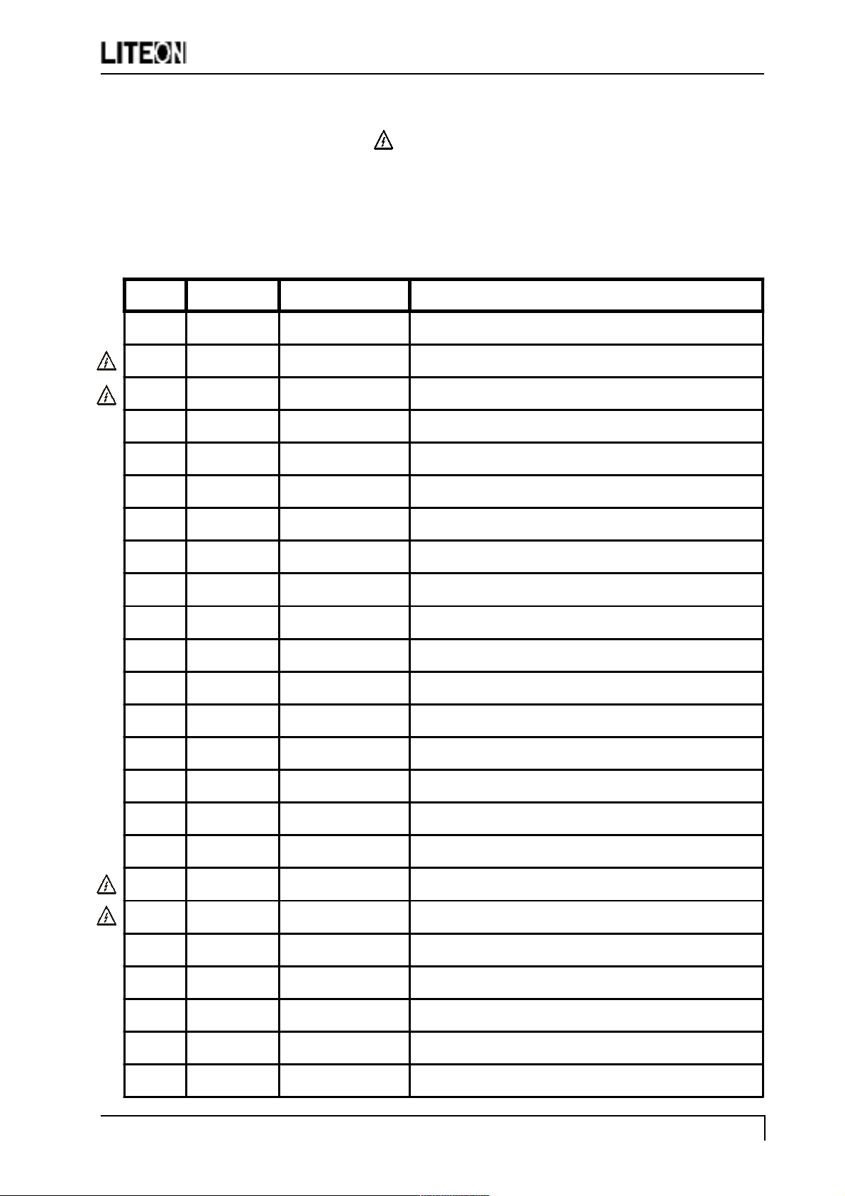
1. Recommended Parts List
Note: 1. The components identified by mark are critical for X-ray safety. Replace these with
only the same parts specified.
2. The components identified by * mark are critical parts.
3. There is only OTP IC at the model beginning (FPR stage or before). When it put in mass
production and there must be Mask coming out. Please checkyou have spart parts need, please
check BOM to get the last release part number and related information.
No. Location Part Number Description
1 V002 6711300030 HARNESS 30P 200mm 20276#28-3
2 * V170 6814002100 LCD L170E3 ACER (B17AAU)
3 * V170 6814002600 LCD HT17E11-100 REV=0 HYDIS (B17AAY)
4 D321 6412001778 DIODE MM4148 SMD GOODARK
5 I301 6444006108 IC MOS M51953AFP 8P SOP
6 * I302 6448015548 IC CPU PROM P87C51RD+IA 44P PL
7 I305 6448016508 IC 24LC16B/SN 8P SOP
8 I312 6448018208 IC 24LC02B 8PIN SOP MICROCHIP
9 * I315 6444007608 IC CMOS gm5020 292P BGA GENESI
10 I319 6444007708 IC CPU SN75LVDS83 56PIN DGG TI
11 I321 6442027308 IC Linear Si4431DY 8P SOP
12 I323 6442023326 IC Linear AIC1084 33CM 3P TO26
13 I324 6442028308 IC Linear Si3025LS 8P SOP SANK
14 L302 6855003500 EMI FILTER EF 1T2012 050T C&C
15 X301 6449002650 CRYSYAL 24MHz AT 49 50pp
16 0000 5114600001 CONTROL BD U170ATUAV(99)
17 D600 6418004401 LED LTL 36EDJP 1(Y)3(G) LITEON
18 * INVA 6716009600 INVERTER DC-AC 12V AMBIT (B17AAU)
19 * INVA 6716010000 INVERTER DC-AC 12V AMBIT T151005 (B17AAY)
20 I332 6442023100 IC-LINEAR TDA7496L 20P
21 L332 6111456131 COIL CHOKE 45uH DRWW10x10L
22 00000 5113800003 CONTROL BD for Mecury
23 00000 5113800013 CONTROL BD for Super Mecury
24 00000 5113800002 CONTROL BD for Eureka
Recommended Spare Parts List Page 1
Page 30

LITE-ON TECHNOLOGY CORP.
5 F, No. 16, Sec. 4, Nanking E. Road, Taipei, Taiwan
Tel: 886-2-25706999 Fax: 886-2-25706888
URL:// www.liteontc.com.tw
Printed in Taiwan
 Loading...