

Page 1
Service Manual
A1454 / A1554NEL
Color Monitor
Page 2
Service Manual V ersions and Revision
No. Vers ion Release Date Revision
1. 1.0 May 28, 1998 Original release
2 1.1 June 19, 1998 4-1- 3 (3)
4-2 - 2 Screen and White Balance Adjustment
6 (15) update model
6 (16) add spare parts
3 1.2 July 8, 1998 2-6 DPMS (Page 9)
3 (Page 10)
Copyright
Copyright 1998 LiteOn T echnology Corp.
All Rights Reserved
This manual may not, in whole or in part, be
copied, photocopied, reproduced, translated, or
converted to any electronic or machine readable
form without prior written permission of LiteOn
T echnology Corp.
A1454 / A1554 NEL Service Manual.
Printed in T aiwan.
T rademarks
LiteOn is a registered trademark of LiteOn
T echnology Corp.
All other trademarks are the property of their
respective owners.
Page 3

A1454 / A1554 NEL
Table of Contents
1. Precautions................................................................................................. 2
2. Product Specifications .............................................................................. 5
3. Operation Theory ...................................................................................... 9
4. Alignments and Adjustments .................................................................... 13
5. Troubleshooting......................................................................................... 17
6. Recommended Spare Parts List ................................................................ 21
7. Block Diagram .......................................................................................... 23
8. Exploded Diagrams..................................................................................... Inserted
9. PCB Diagrams ............................................................................................ Inserted
10. Schematic Diagrams................................................................................... Inserted
1
Page 4
A1454 / A1554 NEL
g
1 Precautions
Follow these safety and servicing precautions to prevent damage and to protect against potential hazards
such as electrical shock and X-rays.
1-1 Safety Precautions
1-1-1 Warnings
1. For safety purpose, do not attempt to modify
the circuit board, and always disconnect the AC
power before performing servicing on the
monitor.
2. Operation of the monitor outside its cabinet or
with the cover removed involves the risk of
shock hazard. Repair work on the monitor
should only be attempted by service personnel
who are thoroughly familiar with all necessary
safety precautions and procedures for working
on high voltage equipment.
3. Do not lift the CRT by the neck. After
completely discharging the high voltage anode,
handle the CRT only when wearing shatterproof
goggles. Try to keep the CRT away from the
body during handling.
4. High voltage should always be kept at the rated
value, no higher. Only when high voltage is
excessive are X-rays capable of penetrating the
shell of the CRT. Operation at high voltages
may also cause failure of the CRT or high
voltage circuitry.
nonmetallic control knobs, insulating materials,
cabinet backs, adjustment and compartment
covers or shields, isolation resistor-capacitor
networks, mechanical insulators, etc.
3. AC Leakage Current Check
Always perform the AC Leakage Current
Check on the exposed metal parts, including
metal cabinets, screwheads and control shafts,
as follows:
a) Plug the AC line cord directly into a rated
AC outlet. Do not use an isolation
transformer during the check.
b) Use an AC voltmeter with at least 5000
ohms per volt sensitivity as follows:
Connect a 1500 ohms, 10 watt resistor
paralleled by a 0.15uF AC capacitor in series
with all exposed metal cabinet parts and a
known earth ground, such as electrical
conduct or electrical ground connected to
earth ground, as shown in the Figure 1-1.
Measure the AC voltage across the
combination of resistor and capacitor .
Figure 1-1. Set Up For AC Leakage Current Check
5. The CRT is especially constructed to limit Xray emission to 0.5mR/HR at 300 microamperes
anode current. To ensure continued X-ray
protection, replace the CR T with only the same
or equivalent type as the original, and adjust the
anode’s voltage to the designated maximum
rating, never to exceed.
1-1-2 Safety Checks
Before returning the monitor to the user, perform
the following safety checks:
1. Inspect to make certain that each lead dress is
not pinched or that hardware is not lodged
between the chassis and other metal parts in
the monitor.
2. Inspect all protective devices such as
2 Precautions2
To kn own
earth
round
0.15ufd
1500 ohm 10 w att
To ex posed m e tal
cabinet part
c) Reverse the AC plug at the AC outlet and
repeat the steps for AC voltage
measurements for each exposed metal part.
d) Voltage reading must not exceed 0.3 volts
RMS, equivalent to 0.2 milliampere AC. Any
value exceeding this limit ill constitute a
potential shock hazard and must be
corrected immediately .
Page 5
A1454 / A1554 NEL
1-1-3 Product Safety Notices
Many electrical and mechanical parts in this chassis have special safety-related characteristics which are often
not evident from visual inspection, the protection afforded by them may not be obtained by replacing them
with components rated for higher voltage, wattage, etc. Before replacing any of these components, consult
the Recommended Spare Parts List given at the end of this manual. Any of the replacements that do not
provide the same safety characteristics may result in shock, fire, X-ray emission or other hazards.
1-2 Servicing Precautions
Warning: An electrolytic capacitor installed with the wrong polarity might explode.
Caution: Before performing servicing covered by this service manual, read and follow the Safety Precautions
section of this manual.
Note: If unforeseen conflict between the following servicing precautions and any of the safety precautions,
always follow the safety precautions
1. Follow closely the servicing precautions printed on the monitor cabinet and chassis.
2. Always unplug the AC power cord from the AC power source before removing or installing any component
or assembly , disconnecting PCB plugs or connectors and connecting a test component in parallel with a
capacitor.
3. When replacing parts or circuit boards, clamp the lead wires around the component before soldering.
4. When replacing a high wattage resistor (>0.5W metal oxide film resistor) in the circuit board, keep the
resistor about 1 cm (1/2 inch) away from the circuit board.
5. Keep wires away from the high voltage or high temperature components.
6. Keep wires in their original positions so as to minimize interference.
7. Always connect a test instrument’s ground lead to the instrument chassis ground before connecting the
positive lead; always remove the instrument’ s ground lead last.
After putting the rear cover back and make sure the monitor is working properly , the Hi-PoT &
Ground Continuity tests MUST BE performed before the monitor is returned to user.
1-3 Hi-Pot T est
1. T est Equipment
Puncture test model PM5530 ADT or KIKUSU TOS-8750 voltage tester or equivalent approved equipment.
Note : The test equipment must be calibrated in regular period.
2. Test Setup
a) Apply voltage : DC 2100 VDC
b) T est duration : 3 seconds
c) Cutoff current should be set to 3 mA
3. Test Procedure
a) Unplug power cord from AC source.
b) Put the power switch of the monitor in the “ON” position.
c) Leave signal cable un-connected.
Precautions
3
3
Page 6

d) Plug monitor power cord to the Hi Pot tester terminals.
e) Turn on tester and watch the indicator or beeper.
f) If the indicator lamp lighten, or beeper beeps, the test fails.
1-4 Ground Continuity T est
1. T est Equipment
AC low ohm tester TOS-6100 or equivalent approved equipment.
Note : The test equipment must be calibrated in regular period.
2. Test Setup
a) Test duration : 3 seconds
b) Set current limit at 25 A
c) The grounding resistance must be less than 0.1 ohm.
3. Test Procedure
a) Plug the monitor power cord to the tester terminals.
A1454 / A1554 NEL
b) Make sure all connections are well-contacted.
c) Turn on monitor power and tester power.
d) Press “Test” button.
e) If green light shows up, means test OK.
If red light shows up, means test fails.
f) If the T ester has a digital display, the resistance value must not exceed 0.1 ohm.
Note : Be sure not to touch the metal portion of the signal cable head during testing.
4 Precautions4
Page 7
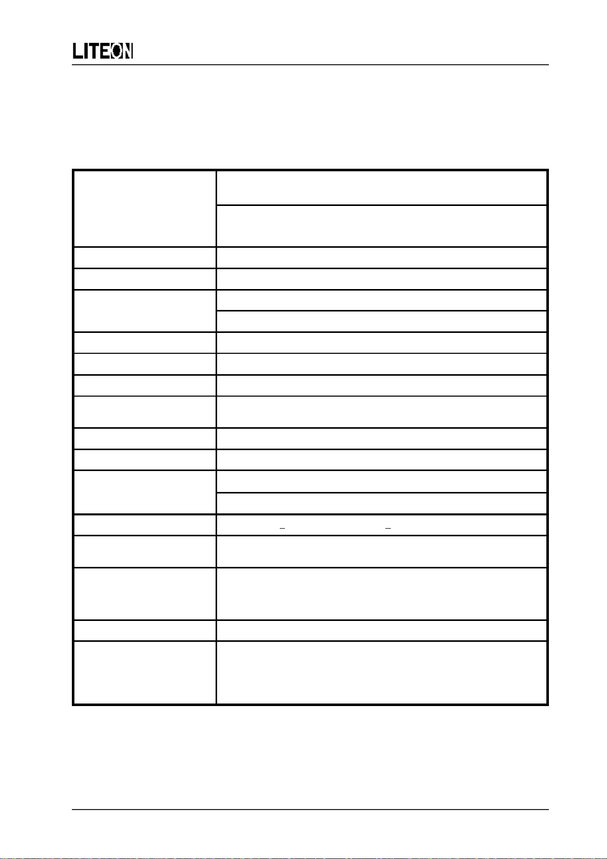
2 Product Specifications
2-1 Specifications
A1454 / A1554 NEL
Picture Tube
Scanning Frequency VGA, Super VGA, 800x600@60/72/75/85 Hz, 1024x768@60 Hz
Maximum Resolution 1024 dots (H) x 768 li nes (V) @60Hz refresh rate
Display Area 14-inch 250 mm (H) x 187 mm ( V) typical
Display Characters 80 char. x 60 rows on a 10 x 10 matrix
Display Colors Analog Input Unlimited Colors
Sync hroni zati n Signal s Se par ate S ync: ho ri zontal /ve rti cal , T TL, pos iti ve o r nega tiv e
Sync hroni zati on Fre quenc ies
Si gnal Co nnecto rs 15 -pi n, D-s hel l co nnecto r
Vi deo Signals Analog : 0.7 Vp-p, RG B p ositive
14-inch (13.3-inch Visual image area),
15-inch (14.0-inch Visual image area)
slote d ma sk, 90 degrees de flectio n, d ot type black matrix, medium s ho rt
persistence phosphor, dark tint, non-glar e/ anti-static screen, 0.28 mm dot
pitch
15-inch 262 mm (H) x 196 mm ( V) typical
Horizontal : 30 to 54 kHz
Vertical : 50 to 120 Hz
Powe r Inp ut
Misconvergence Center Area : <
User Controls Power On/Off, Contrast, Brightness, Vertical Sizs, Vertical Position,
Service Controls PWB-1402 : R-bias (VR910), G-bias (VR940), B-bias (VR970),
Preset Modes 12 (see Tabl e 2-2. Timing Chart)
Environmental Considerations Operati on temperature : 5
14-i nch 7 0 Watts ( nominal ) AC rated vol tage, 100VAC to 264VAC
15-i nch 7 5 Watts ( nominal ) AC rated vol tage, 100VAC to 264VAC
0.3 mm; Corner Area : < 0.4 mm
Horizontal Positi on, Horizontal Size, Pincushion, Trapezoid,
R-gain (VR599), G-gain (VR598)
PWB-1405 : power vol tage adjust (VR801), high voltage ad just (VR80 2),
, focus
o
C to 40oC ambient
o
Storage temperature : 0
Humidity : 5% to 95% ambient
Storage Humidity : 5% to 95% (non-condensi ng)
Altitude : up to 3000m a bove sea l evel
C to 65oC ambient
Note: The above specifications are subject to change without prior notice.
Product Specifications
5
5
Page 8
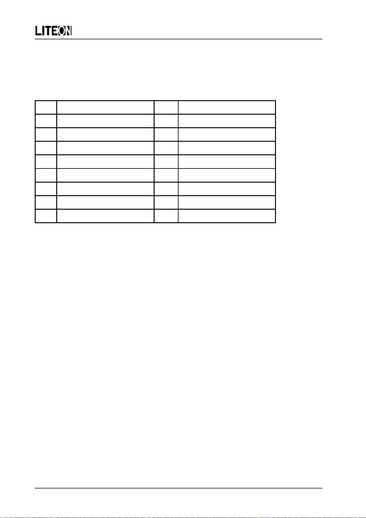
2-2 Signal Cable Pin Connections
Table 2-1. Pin Assignments
Pin Sig nal Pin Sig nal
1 Red video 9 No pin
2 Gr ee n vid eo 1 0 Dig ita l Gr ou nd
3 Blue video 11 Gro und
4 Gr ound 12 SDA
5* Selftest 13 H-Sync
6 Re d gr ound 14 V -Sync /VC L
7 Gr een ground 15 SC L
A1454 / A1554 NEL
8Blue ground
Note: * This pin is used for selftest detection. Connect this pin to ground at the PC end.
6 Product Specifications6
Page 9
A1454 / A1554 NEL
2-3 Timing Chart
This section of the service manual describes the timing that the computer industry recognizes as standard for
computer-generated video signals.
Table 2-2. T iming Chart
Mode 123456789101112
H. Do ts 720 720 640 640 640 800 800 800 800 640 1024 800
V. Dot s 350 400 480 480 480 600 600 600 600 480 768 600
H-freq (k Hz) 31.47 31.47 31.47 37.86 37.5 35.16 37.88 46.875 48.08 43.3 48.36 53.674
Sync Polarity +-- - -+/-+ + + - - +
A Perio d us 31.78 31.78 31.78 26.413 26.666 28.44 26.4 21.333 20.8 23.11 20.677 18.6
B Blking us 6.356 6.356 6.356 6.095 6.35 6.22 6.4 5.172 4.8 5.333 4.923 4.409
C Sy nc us 3.81 3.81 3.81 1.27 2.07 2 3.2 1.616 2.4 1.556 2.09 1.138
D B.P. us 1.907 1.907 1.907 4.06 3.81 3.556 2.2 3.232 1.28 2.222 2.462 2.702
E Acti ve us 25.42 25.42 25.42 20.317 20.32 22.22 20 16.162 16 17.778 15.75 14.222
F F.P. us 0.636 0.636 0.636 0.76 0.51 0.667 1 0.323 1.12 1.556 0.369 0.569
V-freq (H z) 70.08 70.08 59.95 72.81 75 56.25 60.32 75 72.18 85 60 85
Sync Polarity -+- - - +/-+ + + - - +
G Period ms 14.27 14.27 16.68 13.735 13.33 17.78 16.58 13.333 13.87 11.764 16.67 11.8
H Blking ms 3.146 1.557 1.43 1.057 0.533 0.711 0.739 0.533 1.373 0.67 0.786 0.578
I Sync ms 0.064 0.064 0.064 0.079 0.08 0.057 0.106 0.064 0.125 0.069 0.124 0.056
J B.P. ms 1.87 1.08 1.02 0.74 0.407 0.626 0.607 0.448 0.478 0.578 0.6 0.503
K Active ms 11.12 12.71 15.25 12.678 12.8 17.07 15.84 12.8 12.51 11.093 15.88 11.179
L F. P. ms 1.21 0.413 0.35 0.238 0.026 0.0284 0.026 0.021 0.770 0.023 0.062 0.019
Video
A
E
B
F
Sync
H orizontal
D
C
H.Parameters:
A: Period B: Blanking Time
C: Sync Width D:Back Porch
E : Active Time F: Front Porch
Seperate Sync
Ver tic a l
V .Parameters:
G : Period H: Blanking Time
I: Sync W idth J: Back Porch
K: Active Time L: Front Porch
K
Video
J
Sync
I
G
H
L
Product Specifications
7
7
Page 10
A1454 / A1554 NEL
2-4 Display Power Management Signaling (DPMS)
Note: These power-saving states exceed the Environmental Protection Agency (EPA) Energy Star
requirements and the Video Electronics Standard Association (VESA) for Display Power
Management Signaling (DPMS) .
T able 2-3. Display Power Management Signaling (DPMS)
State LED Color H-Sync V-Sync Power
Co ns umptio n
ON Green Pulse Pulse Normal
STANDBY Yellow No Pulse Pulse <15 watts
SUSPEND Yellow Pulse No Pulse <15 watts
OFF Amber No Pulse No Pulse <5 watts
8 Product Specifications8
Page 11

A1454 / A1554 NEL
3 Operation Theory
This is a fully digital multi-sync color monitor that is compliant with DDC1 and 2B Plug and Play VESA
standard and offers the following main features.
3-1 Main Features
1. Simplified design with minimum components.
2
2. The NOVATEK NT68P61A processor-- that has I
brightness-- offers the functions for: (a) Contrast, (b) Brightness, (c) H-size, (d) H-position, (e) V-size, (f)
V-position, (g) Pincushion, and (h) Trapezoid.
C BUS controlled geometric correction, contrast and
In addition, it also offers more functions as: (a) Sync. processor, I/P and O/P, (b) Mute, (c) Power saving
- Suspend & Stand-By , (d) Power saving override, (e) DDC1/2B, (f) I
signal cable (g) CS1/CS2 for linearity and size compensation.
3. Stores up to 12 factory preset modes and offers 6 user modes. Recall factory modes by pressing together
“+” and “-” keys from the front panel. Use “Select” key to select a parameter and “+” and “-” for
adjusting the value of the parameter. User setting data are stored automatically.
4. Powerful PHILIPS TDA4853 and TDA4866 present the following useful functions: (a) Pincushion, (b)
Trapezoid, (c) V-Position, (d) V-Size, (e) Vertical’s “C” and “S” correction -- factory adjust, (f) Pincushion’ s
V. position correction, (g) Corner correction -- factory adjust, (h) Pincushion unbalance correction -factory adjust, (i) Parallelogram distortion -- factory adjust, (j) Moire cancellation -- factory adjust, (k) Xray protection, and (l) Full horizontal plus with vertical auto sync capability .
5. Software controlled auto shut off function activated if fH < = 29 kHz and fH > = 56 kHz.
6. Full range AC input and simplified line filter design.
2
C Bus for auto-alignment through
3-2 Microcontrol Section
1. This monitor uses NOVATEK NT68P61 CPU. It contains a 6502 8-bit CPU core, 256 bytes of RAM
used as working RAM and stack area, 24k bytes of OTP ROM, 14-channel 8 bit PWM D/A converter,
2-channel A/D converters for key detection saving I/O pins, internal H. sync and V. sync signals processor
providing mode detection, and an I2C bus interface. When H/V sync through D-Sub signal cable enter pin
39 and pin 40, the CPU marks frequency polarity detection and calculate and send to H/V sync OUT.
Then CPU reads the data from I703 and write to device 4854 and some DAC in CPU. the above
operation takes about 500 ms.
2. There are 12 factory preset modes and 6 user modes. There are 8 functions, Contrast, Brightness, H.
Size, H. Position, V. Size, V. Position, Pincushion, and Trapezoid, all controlled by panel keys which can
be adjusted by user.
3. The user control parameters are selected in sequence listed as above by LEDs. When pressing “select”,
the function will be selected one by one. When a particular parameter is chosen, use “+” and “-” button
to adjust the value. LED will flash when reaching extreme value, which means the value cannot be
increased or decreased anymore. There are seven functions which can be controlled only by internal
setting. Through internal setting user can modify the factory preset data.
4. The pin 24 and pin 25 are used for ATE and DDC function. The DDC1 and DDC2 are implemented in
CPU. When power on the CPU is initial in DDC1 mode. At DDC1 mode when V. sync in, the data will
be sent out one by one. When SCL is lowized, the CPU will enter the DDC2 mode. In DDC2 mode, after
receiving A0 0 A1, the EDID data will be sent out. When CPU receive C6 as slave address, the CPU will
operate in ATE mode which is used for auto-alignment. After alignment the data will be stored in I703.
Operation Theory
9
Page 12

3-3 Deflection Section
1. I2C -- autosync deflection controller is TDA4853.
A1454 / A1554 NEL
2. The TDA4853 is a high performance and efficient solution for autosync monitors. All functions are
controllable by I
control all functions.
2
C bus. SDA and SCL signals come from microprocessor feed to pin 19 and pin 18 to
3-3-1 Horizontal Section
1. The oscillator is driven by the currents in R419 and R420. The minimum oscillator frequency is determined
by R419 and the maximum frequency is determined by R420.
2. Horizontal sync comes into pin 15 through R318. And horizontal flybok pulse comes into pin 1 through
R401, R402 and by pass filter C403 from pin 6 of FBT for AFC loop.
3. Horizontal driver (pin8) O/P to Q401 via C410.
3-3-2 V ertical Section
1. Vertical sync comes into pin 14 through R317.
2. The free running frequency is determined by R301 and C301.
3-3-3 V ertical O/P section
1. The differential output currents from pin 13 of Vout1 and pin 12 of V out2 can be directly coupled to the
vertical deflection booster pin 1 and pin 2 of TDA4866.
2. The TDA4866 has two output stages which are current driven in opposite phase and operate in combination
with the deflection coil in a full bridge configuration.
3-3-4 E-W/T rapezoid and H. Width Controls
1. The horizontal O/P stage uses diode modulator D419, D423, C411, C412, L409 and C418 for East-West
(Pincushion) Trapezoid and H. width controls.
2. The scan current is determined by B
is accomplished by Darlington pair Q418 and Q419 by coupling a parabola waveform from pin 11 of
TDA4853. The H. width size corner correction and trapezoid are also accomplished by this pin 11.
+
minus Vm ( the voltage of C418) values and the pincushion control
3-3-5 X-Ray Protection
1. T o avoid X-ray hazard, a DC voltage generated by pin 6 of FBT and rectified by D408, C432 and divided
by R403, R404 and R405 come into pin 2 of TDA4853.
2. If this voltage is higher than 6.39 V , then TDA4853 will be activated to float HUNLOCK (pin17), H. DR V(
pin 8), B DR V (pin 6), VOUT1 (pin 12), VOUT2 (pin13). After that all deflection circuit stop working.
3-3-6 G1, Blanking and Brightness
1. The vertical blanking signal comes from two ways. One is from pin 8 of I301 (TDA4866), the other is
from vertical sync (pin 32 of I701). This two positive vertical pulses through Q406 amplified and converted
into negative pulse and sent to G1 for vertical blanking.
2. In protection mode or an out of range situation HUNLock will send 5 V pulse to saturate Q405 and open
Q408 then G1 will go down to -140V. During the mode change, Mute acts as same as HUNLock’s.
3. The brightness is controlled by CPU pin 1 comes into PNP transistor Q408, low voltage causes high
10 Operation Theory
Page 13

A1454 / A1554 NEL
current to get brighter raster, high voltage gets lower brightness.
3-4 Power Supply Section
3-4-1 AC Rectifier
The circuit can accept 90 V to 264 V AC input through D801~D804 bridge diodes and C808 filtering to get
DC 126 V~364 V for power conversion in T802.
3-4-2 Line Filter
It consists of C801, C802, C803, C816 and T801 and meets EMI regulation.
3-4-3 Power LED Status
1. The LED has 3 leads common cathode with green and amber colors for different power saving indications.
It is controlled by CPU.
2. Normal : Green light
Amber LED is off because CPU pin10 is high and pin 9 is low , only green LED is turned on.
3. Standby / Suspend : Y ellow light
CPU pin 9 and pin 10 are low, then green and amber LED are turned on. That is yellow.
4. Off Mode : Amber light
CPU pin 9 is high and pin 10 is low, then green is of f and amber is on.
3-4-4 Auto Degaussing
1. A1454NEL : When SMPS works, the 6.3 V power source is applied to Q802 and CPU let Q802 turn on
a few seconds, then drive the armature of RL801 to perform the degaussing function.
2. A1554NEL : When power switch S801 on, the AC current flows through R862, D816 (D817) and
degaussing coil preforms the degaussing function.
3-4-5 PWM Control
1. Start Up
The I801 gets power from R807, R817, C812 and pin 7 voltage reaches 16 V for starting up. The I801
starts oscillation at 22 kHz, sawtooth on pin 4 and pin 6 output to drive Q803/T802. Once Q803 switches
on, D806, C804 set up an 15 V to keep I801 working through D808 auxiliary voltage.
2. Regulation
The DC O/P voltage is proportional to the auxiliary voltage, so I801 pin 2 senses the feedback voltage
from the divider R802, R823, VR801 and R821 to compare with built-in 2.5 volts reference voltage for
error amplifier operation. Finally pin 6 can modulate the different duty cycle by VR801 setting to achieve
regulation purpose.
Operation Theory
11
Page 14

A1454 / A1554 NEL
3-4-6 Synchronization
1. Normal Mode
The sync pulse from FBT (31 kHz~54 kHz) via C815, R826, D824 and R816 to pin 4 of I801 to keep I801
synchronized with horizontal sync input frequency .
2. Power Saving Modes: Standby/Suspend
Because there is no pulse from FBT, so the free-run frequency is decided by R815 and C814 and the
SMPS works at 22 kHz.
3. Override
The horizontal free run frequency is about 41 kHz under override condition, SMPS is synchronized to this
frequency .
3-4-7 O.V . P .
If the auxiliary voltage is higher than zener voltage ZD807 (18 volts) and makes pin 3 of I801 higher than
1 V, pin 6 duty cycle is limited to have the OVP activated.
3-4-8 O.P.P.
The excess current of T802 through R813 can develop enough voltage to pin 3 then limit the power delivered
because the pin 6 duty cycle is limited too.
3-4-9 Step Up Power Supply For FBT
1. The B+ of FBT is proportional to horizontal frequency , that is higher frequency , higher voltage. The basic
voltage is 75 volts from T802 pin 9 via D840, L812 and the gate control of Q807 comes from I401 pin 6 via
Q808, Q809 and Q810. The duty cycle is controlled by C843, C462, R489, R846 and R856, R857, R858
VR802 combination ratio.
2. The regulation and boost up (from 77 V to 92 V or more, on demand). The H.V. is set at 24.5 kV (zero
beam) by VR802 which senses the secondary O/P from FBT . The booster comprises Q807, L801, D820,
C425 and I802 to offer the required B+ for different frequency modes.
3-5 Video Amplifier Section
1. RGB signal inputs are terminated by R502, R532 and R562 then pass through the coupling capacitors
C501, C531 and C561 to the IC501 MM1375 pre-amplifier .
2. The amplifier RGB signals (0~3 Vpp) are adjusted by VR599 (R), VR598 (G). Pin 9 is for DC contrast
control input, pin 11 is for clamp pulse which comes from pin 16 of TDA4853 to set up the equal clamp
level.
3. The video output stages are cascode amplifiers with buffer of complementary emitter followers, the stray
capacitance is so small that the load resistor R906, R911, R936, R941, R966 and R971 can be 3.6 k ohm
and the power dissipation is minimized.
4. The RGB cathodes cut off are adjusted by VR910, VR940 and VR970.
5. Under override condition, the self test signal is supplied from pin 1 of CPU, the default value is about 1
volt. In this condition, G1 will increase 10 volts then get about 6 FL light out put.
12 Operation Theory
Page 15

A1454 / A1554 NEL
4 Alignments and Adjustments
This section of the service manual explains how to make permanent adjustments to the monitor settings.
4-1 General Adjustments
4-1-1 Adjustment Conditions
a) Power Supply
Apply AC 115 V or 220 V
b) Warm-up T ime
The monitor must be powered on for 15 minutes before starting any alignment, but requires 30 minutes of
warm-up time for convergence adjustment.
c) Signal Input
1. Video: RGB Analog, 0.7 Vp-p, positive
2. Synchronization: Horizontal and vertical TTL signal, separate, positive or negative
3. All adjustments should be made using a signal of FH = 31.468 kHz, FV = 60 Hz, unless otherwise
defined.
4-1-2 Equipment Required
The following equipments are necessary for adjustment procedures:
1. Volt-ohm-A meter (Sanwa FD-750C or equivalent)
2. 30 kV high voltage probe (HP3411 1A)
3. Oscilloscope (TEK2235 or equivalent)
4. Minolta Color Analyzer II
5. Signal generator (IBM PC with proper display cards or Chroma 2000)
6. Screwdriver
4-1-3 Switching Power Supply and Regulator Adjustment
The regulated B+ control has been preset in the factory and needs no adjustment. However, if any repair is
made on the power supply section, the following readjustment procedures are recommended:
1. Allow the monitor to warm-up for about 15 minutes.
2. Apply VGA (1024 x 768 @ 48.36 kHz/60 Hz) signal to the monitor.
3. Connect a DC voltage meter to D814 “-” (TP1 on the control PCB), and adjust VR801 for 13.3 + 0.2
V DC, 13.3 - 0 V DC.
4. If a fuse is broken during adjustment, remember to replace it with the exact same type of fuse.
Alignments and Adjustments
13
Page 16

A1454 / A1554 NEL
4-2 Alignment Procedures
4-2-1 High V oltage Adjustment
CONDITION
Display image : Crosshatch pattern
PROCEDURE
Connect DC meter to TP3 and adjust VR802 to obtain a DC voltage of 152 ± 1V DC for CPT CRT
M34AF A83x8. (M36AES83x-1)
4-2-2 Screen and White Balance Adjustment
CONDITION
Press “+”, “-” and “Select” buttons simultaneously when switching the power “On”.
Drive VRs : VR598, VR599
Bias VRs : VR910, VR940, VR970
Display image : No video
PROCEDURE
1-a. 14” Set brightness to -35 V at G1 and G2=530 V contrast to maximum.
or
15” Set brightness to -35 V at G1 and G2=600 V contrast to maximum.
1-b Adjust VR910, VR940 and VR970 to maximum.
1-c Adjust VR940 to raster just distinguish for green gun.
1-d Adjust brightness to raster light outpert to get 0.9 ~ 1.1 FL.
1-e Adjust VR910 to get x=280 ± 5 and VR970 to get y=280 ± 5
CONDITION
Display image : 50 mm x 50 mm white block pattern
PROCEDURE
2-a. Set brightness to cut-off and G1=-35 V
2-b Adjust contrast to get about 43 FL.
2-c. Adjust VR598 for y=0.311 and then adjust VR599 for x=0.281.
2-d Check item 2-b and 2-c again. If not, then adjust contrast VR to get 43 ± 1 FL light outpert.
CONDITION
Display image : Full white pattern
PROCEDURE
3-a. Set brightness to cut-off and contrast to maximum.
3-b. Adjust VR402 to 28FL +2/-0 FL.
4-a. Check the white balance in the VGA mode at 5 FL and 28 FL.
4-b. Repeat all the procedure in 4-2-2 section until the best white balance is obtained, then power off.
14 Alignments and Adjustments
Page 17

A1454 / A1554 NEL
4-2-3 Focus Adjustment
CONDITION
Display image : “e” character pattern
PROCEDURE
1. Set brightness and contrast used for a normal display.
2. Adjust the static focus control on the high voltage resistor block to obtain the best focus over the entire
display area.
4-2-4 Static Convergence Adjustments
Static convergence involves alignment of the red, blue and green lines in the center area of the display .
Note : The monitor requires 30 minutes of warm-up time for convergence adjustment.
CONDITION
Display image : Crosshatch pattern
W arm-up Time : 30 minutes
PROCEDURE
1. Set brightness and contrast to display a well-defined pattern.
2. Ensure the convergence magnet rings are correctly positioned on the CRT.
Figure 4-1. Convergence Magnets on the CR T
1
11
+
P
8 7 6 5 4 3 2
10
1) Setup Bolt 2) Bow Magnet 3) Band 4) 2-Pole Magnet
5) Spacer 7) Spacer
9) Holder
6) 4-Pole Magnet
9
11) Tabs10) Band
3. Rotate the individual rings of 4-pole convergence magnets by changing the spacing between the 2 tabs to
converge the vertical red and blue lines at the center of the screen.
CRT
FRONT
8) 6-Pole Magnet
4. Rotate the pair of rings of 4-pole convergence magnets by maintaining spacing between the 2 tabs to
converge the horizontal red and blue lines at the center of the screen.
5. Rotate the individual rings of 6-pole convergence magnets by changing the spacing between the 2 tabs to
converge the vertical red, blue and green lines.
6. Rotate the pair of rings of 6-pole convergence magnets by maintaining spacing between the 2 tabs to
converge the horizontal red, blue and green lines.
7. Repeat the steps from 3~6 until the best convergence is obtained.
Alignments and Adjustments
15
Page 18

Figure 4-2. 4-pole and 6-pole Magnets Movement
Blue Red
A1454 / A1554 NEL
Red/
Blue Gree n
Blue
Red
4-pole magn ets
movement
Red/
Blue
Green
6-pole magn ets
movement
Note : The 4-pole magnets and the 6-pole magnets interact, making dot movement complex.
4-2-5 Degaussing
Degaussing is required when poor color impurity appears on the screen. This monitor uses an automatic
degaussing circuit that is activated when the power is on. The automatic degaussing will be fully functional
after the monitor has been in operation for 20 minutes.
The degaussing effect is confined to the picture tube since the coils are mounted at the back of the tube.
Should any part of the chassis or cabinet becomes magnetized, it is necessary to degauss the affected area
with a manual degaussing coil.
4-2-6 Manual Degaussing
1. Apply line voltage to the degaussing coil and move it in a rotary motion over the front, sides, and top of the
monitor . The coil should be kept away from the rear of the monitor to avoid damaging the magnetic neck
components.
2. Slowly rotate and move the coil away from the monitor to about 6 feet beyond the point where no effect
on the CR T will be noticeable.
For proper degaussing, it is essential that the field be gradually reduced by moving the coil slowly away from
the monitor . The degaussing coil must never be shut off or disconnected while near the monitor, as this would
introduce a strong field instead of canceling the effect of the stray fields.
16 Alignments and Adjustments
Page 19

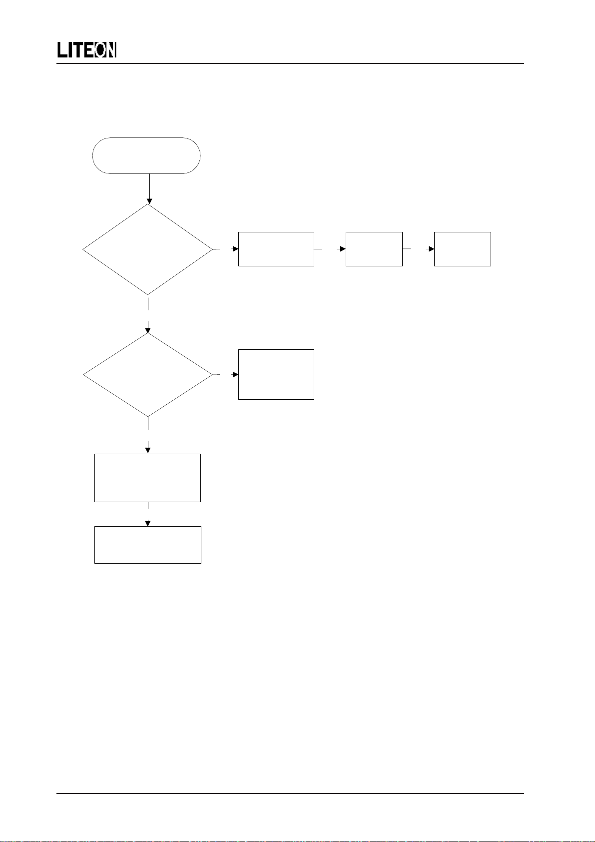
5 T roubleshooting
5-1 No Raster
A1454 / A1554 NEL
No Raster
Measure
voltage of B+ at
T402 pin 3 on
PWB-MAIN
0 V
Short Circuit
at load?
Yes
Check DC B+ line,
Q807, F801
Normal
(83 V, 31.5 kHz)
Check voltage of
No
Check AC I/P
on T801
I801, R813,
R805, R809,
Q803, D806,
D808, D813,
D814, D815, D810
cathode, heater,
Grid 1, Grid 2,
Yes
Check
High
(100 V or more)
Check I401,
Q402, Q401
etc.
No
Check
D801, D802,
D803, D804
T r oubleshooting
17
Page 20

5-2 Function Key Abnormal
Function Key Abnormal
A1454 / A1554 NEL
Check I701 and
I702 missing?
No
Power
ON/OFF again and
check X701,
oscillator OK?
Yes
Check
I702 EEPROM
content OK?
Yes
Yes
No
No
Put on
I701, I702
Replace X701
Replace I702 or
do ATE again
Replace I701 and
check uP OK?
Yes
Replace Q702
No
Replace I701
18 T roubleshooting
Page 21

5-3 Vertical Scan (Raster is one horizontal line)
Vertical Scan Abnormal
A1454 / A1554 NEL
Check voltage of
pin 3 at I301
(about 14 V)
Yes
Check
pin 4 or pin 6
waveform at I301
Normal
Check R311 short ?
No
Abnormal
Ckeck or replace
I301.
Check pin 12 &
pin 13 waveform
at I401
OK
Replace I301
T r oubleshooting
Still no vertical scan
Check or replace CRT
19
Page 22
5-4 R.G.B. Video Amplifier Abnormal
RGB Video AMP
Abnormal
A1454NEL
Check
the waveform at the I501
pin 17, pin 14, pin 20
Yes
Check
I902, Q932, Q962
collector voltage (normally
about 75V)
Yes
Video signal present at
the pin of the CRT
R.G.B. Cathode
Yes
No
No
(pin8, pin19)
Check I501,
R.G.B. O/P
voltage Q901,
Q931, Q961
Check B+
Yes
Check the
waveform at
pin 1, 3, 6
Yes
Check I501
Defective cut-off circuit
(DC restore)
20 T roubleshooting
Page 23

A1454NEL
6 Recommended Parts List
Note: The components identified by “ “ mark are critical for X-ray safety. Replace these with only
the same parts specified.
No. Location Part Number D e scription M odel
1
C417 6326239443 MPP uF 0.39 250V H F P=22.5HJC both
2
C808 6312615102 ALU uF 150 400V F 85C 25x31 both
D801 D802
3
D803 D804
4
D814 D815 6412002027 DIO DE FUF 5404AMP T52 3A/400V both
5
D820 6412002017 DIODE UF3004M T52 3A/400V 50nS both
6
D841 6412018400 DIODE SM- 3AP6 3A/600V O RIGIN both
6412010907 DIODE LT2A06 T52 2A/800V both
7
F801A 6851504050 FUSE TIME LAG H-BRK 4A/250V both
8
I301 6442012300 IC TDA4866 9P (PHILIPS) both
9
I401 6442022500 IC TDA4853 32P SDIP PHILIPS both
10
I501 6442021400 IC MM1375 22P SDIP (MITSUMI) both
11
I701 6448012200 IC NT68P61A 40P PDIP (NOVATEK) both
12
I702 6448007900 IC 24C04A/P (MIC ROCHIP) both
13
I801 6442022000 IC KA3842A 8P PDIP SAM SUNG both
14 L404 6111504130 COIL C HOK E 5mH K DR10x16 both
15 L405 6119004900 C OIL LINEAR TLN-1049 A1554
16 L405 6119004103 C OIL LINEAR TLN-1041 (C) A1454
17 L409 6111185131 COIL C HOK E L=188uH DR10x20 both
18 Q 402 6421003200 TR N PN 2SC 5339 (TOSHIBA) both
Q421 Q430
19
Q807
6426006400 FET N-C HNL IRFS630A SAMSUNG both
20
Q803 6426006700
21
R403 6224230124 MF KO HM 30.1 1/4W F A1454
22
R403 6224290914 MF KO HM 9.09 1/4W F T26 A1554
23
R404 6224286624 MF KO HM 86.6 1/4W F A1454
Recommended Spare Parts List
FET N- CHNL SSS7N60A
(SAMS UN G)
both
21
Page 24

A1454 / A1554 NEL
N o. Location Part Numbe r D escription M odel
24
R404 6224228024 M F KO HM 28 1/4W F T26 A1554
25
R405 6224216924 M F KO HM 16.9 1/4W F A1454
26
R405 6224256014 M F KO HM 5.6 1/4W F T26 A1554
27
R803 6203090002 PO SISTOR 9 O HM Q 2PIN PITC H=10 A1554
28
R804 6201160011 THERMISTOR 16 O HM 2A P=5 UEI both
29
R818 6220327852 FS O HM 0.27 1W J HO R both
30 R862
31 T401
32 T402
33 T801
34 T802 6131041900 X'FRM ER PW R TPW -1064 EE40 DEI both
35 X701 6449000700 CRYSTAL HC 49/U 8M HZ 50ppm 7pF both
6203090017
6135000103 X'FRM ER H OR DRIVE THD-1001(D) both
6133054020 F BT TFB-5402 C F1095 LIEN CHAN G both
6138001621 LINE FILTER TLF -1016A 16mH AXIS both
PO SISTOR 9 OHM
C3R9R0Q 27AWLSN
A1454
22 Recommended Spare Parts List
Page 25
Page 26

Page 27

Page 28

Page 29

Page 30

Page 31

LITE-ON TECHNOLOGY CORP.
5 F, No. 16, Sec. 4, Nanking E. Road, Taipei, Taiwan
T el: 886-2-25706999 Fax: 886-2-25706888
URL:// www.liteontc.com.tw
Printed in Taiwan
 Loading...