

Page 1

LITE-ON DCC
RELEASE
LITE-ON Technology Corp. / Optoelectronics
No.90,Chien 1 Road, Chung Ho, New Taipei City 23585, Taiwan, R.O.C.
Tel: 886-2-2222-6181 Fax: 886-2-2221-1948 / 886-2-2221-0660
http://www.liteon.com/opto
Photocoupler
Product Data Sheet
6N135-L / 6N136-L series
Spec No.: DS70-2008-0032
Effective Date: 04/12/2016
Revision: A
BNS-OD-FC001/A4
Page 2
Photocoupler
6N135-L 6N136-L series
Part No. : 6N135-L 6N136-L series
BNS-OD-FC002/A4
1. DESCRIPTION
The 6N135/ 6N136-L consists of a high efficient AlGaAs Light Emitting Diode and a high speed optical detector. This design
provides excellent AC and DC isolation between the input and output sides of the Optocoupler. Connection for the bias of the photodiode
improves the speed that of a conventional phototransistor coupler by reducing the base-collector capacitances. The internal shield
ensures high common mode transient immunity. A guaranteed common mode transient immunity is up to 1KV/μsec.
1.1 Features
High speed – 1MBd typical
Available in Dual-in-line, Wide lead spacing, Surface mounting package.
Storable output.
UL, CSA approval
1.2 Applications
Isolation in line receivers
Digital isolation for A/D, D/A conversion
Ground loop elimination
Feedback Element in Switching Mode Power Supplier
Pulse transformer replacement
Power transistor isolation in motor drives
Interface between Microprocessor system, computer and their peripheral
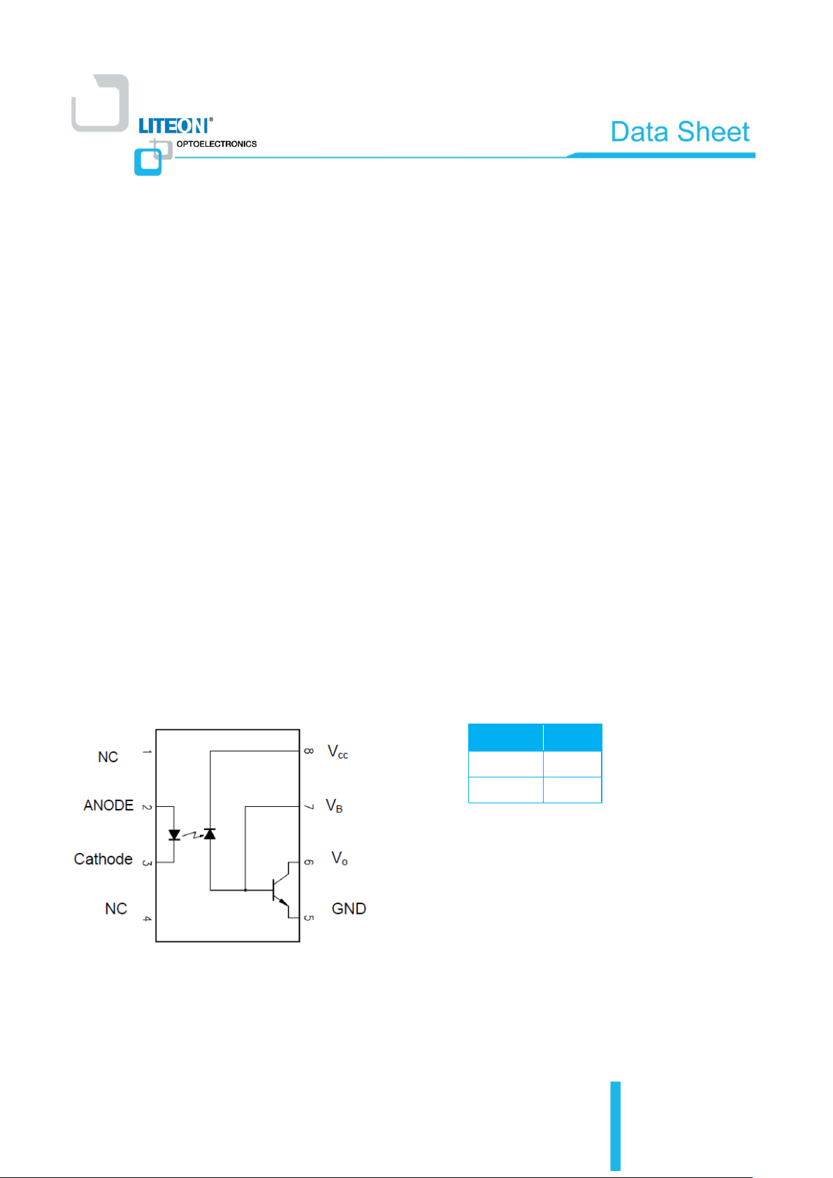
1.3 Functional Diagram
A 0.1μF bypass Capacitor must be connected between Pin8 and Pin5
Truth Table (Positive Logic)
LED
OUT
ON L OFF
H
1/15
Page 3
Photocoupler
6N135-L 6N136-L series
Part No. : 6N135-L 6N136-L series
BNS-OD-FC002/A4
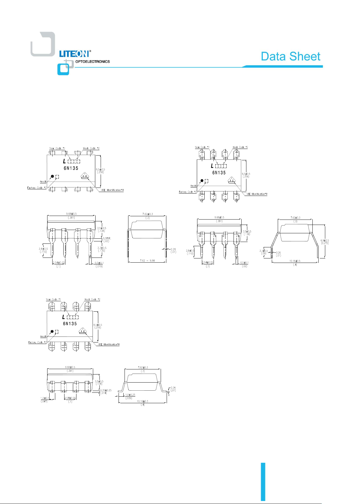
2. PACKAGE DIMENSIONS
2.1 6N135-L 2.2 6N135M-L
2.3 6N135S-L
Notes :
1. Year date code.
2. 2-digit work week.
3. Factory identification mark shall be marked
(Y: Thailand , W: China-CZ)
4. For VDE option.
Dimensions in millimeters (inches).
2/15
Page 4
Photocoupler
6N135-L 6N136-L series
Part No. : 6N135-L 6N136-L series
BNS-OD-FC002/A4
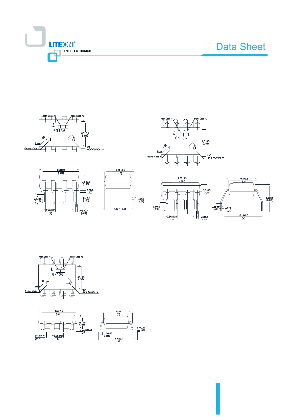
2.4 6N136-L 2.5 6N136M-L
2.6 6N136S-L
Notes :
1. Year date code.
2. 2-digit work week.
3. Factory identification mark shall be marked
(Y: Thailand , W: China-CZ)
4. For VDE option.
Dimensions in millimeters (inches).
3/15
Page 5
Photocoupler
6N135-L 6N136-L series
Part No. : 6N135-L 6N136-L series
BNS-OD-FC002/A4
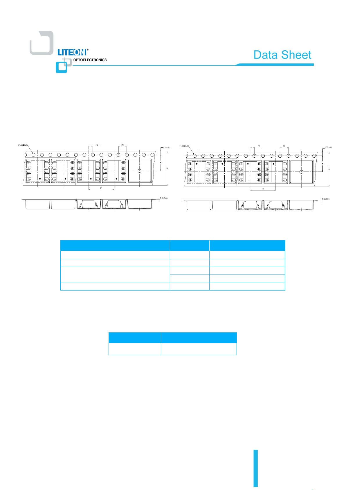
3. TAPING DIMENSIONS
3.1 6N135S-TA-L/ 6N136S-TA-L 3.2 6N135S-TA1-L/ 6N136S-TA1-L
3.3 Quantities Per Reel
Description
Symbol
Dimension in mm (inch)
Tape wide W 16±0.3 (0.63)
Pitch of sprocket holes
P0
4±0.1 (0.15)
Distance of compartment
F
7.5±0.1 (0.295)
P2
2±0.1 (0.079)
Distance of compartment to compartment
P1
12±0.1 (0.472)
Package Type
TA / TA1
Quantities (pcs)
1000
4/15
Page 6
Photocoupler
6N135-L 6N136-L series
Part No. : 6N135-L 6N136-L series
BNS-OD-FC002/A4
4. RATING AND CHARACTERISTICS
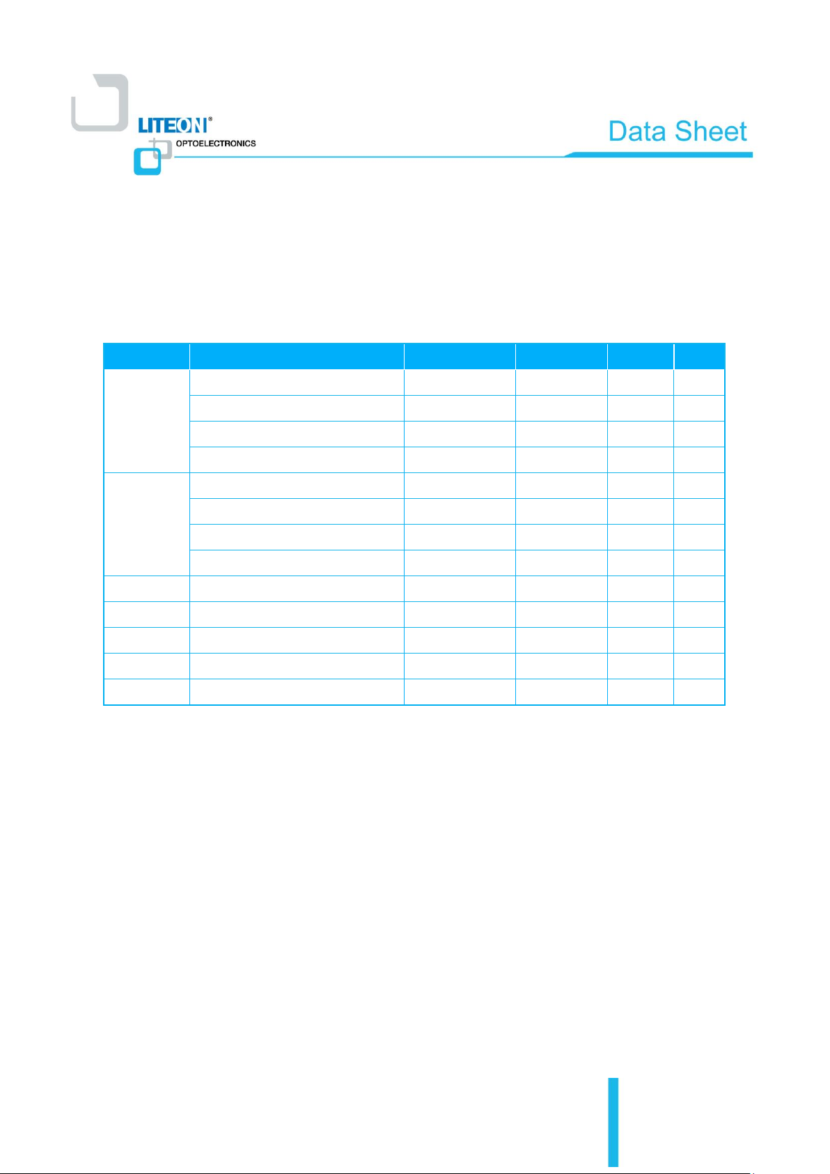
4.1 Absolute Maximum Ratings at Ta=25°C *1
Parameter
Symbol
Rating
Unit
Note
Input
Average Forward Input Current
IF
25
mA 2 Reverse Input Voltage
VR
5 V
Power Dissipation
PI
45
mW Junction temperature
TJ
125
o
C
Output
Output Collector Current
IO
8
mA Output Collector Voltage
VO
20
V Output Collector Power Dissipation
Po
100
mW Junction temperature
TJ
125
o
C
Isolation Voltage
V
ISO
5000
V
rms
Supply Voltage
VCC
15
V
Operating Temperature
T
opr
-40 ~ +85
oC
Storage Temperature
T
stg
-55 ~ +125
oC
Lead Solder Temperature *2
T
sol
260
oC
1. Ambient temperature = 25oC, unless otherwise specified. Stresses exceeding the absolute maximum ratings
can cause permanent damage to the device. Exposure to absolute maximum ratings for long periods of time
can adversely affect reliability.
2. 260oC for 10 seconds. Refer to Lead Free Reflow Profile.
5/15
Page 7
Photocoupler
6N135-L 6N136-L series
Part No. : 6N135-L 6N136-L series
BNS-OD-FC002/A4
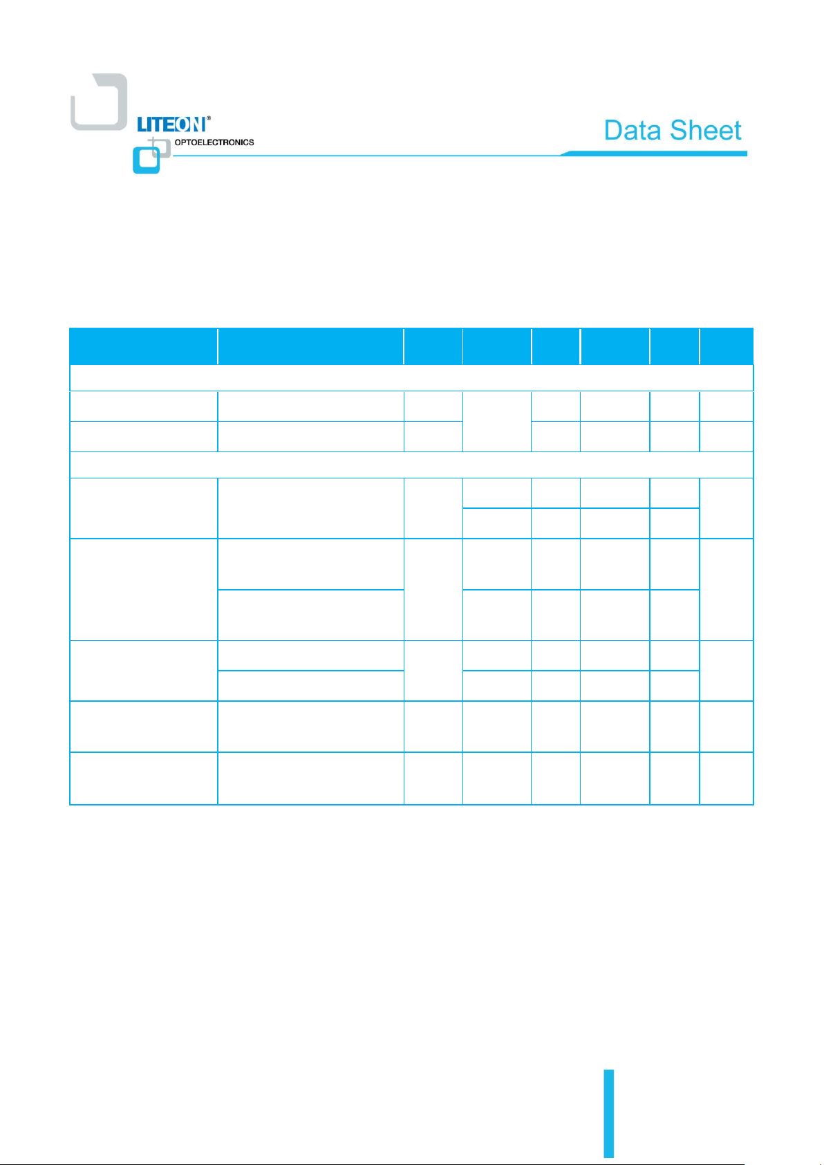
4.2 ELECTRICAL OPTICAL CHARACTERISTICS at TA = 25°C
Parameters
Test Condition
Symbol
Device
Min
Typ
Max
Units
Input
Input Forward Voltage
IF =16mA, TA=25℃
V
F
6N135
6N136
1.4
1.7
V
Input Reverse Voltage
IR = 10μA TA=25℃
BVR
5
- - V
Detector
Current transfer ratio
IF=16mA; Vo=0.4V;
VCC=4.5V; TA=25℃
CTR
6N135 7 18
50
%
6N136
19
24
50
Logic low output voltage
IF=16mA;Vcc=4.5V;
Io=1.1mA; TA=25℃
V
OL
6N135
-
0.18
0.4
V
IF=16mA;Vcc=4.5V;
Io=3mA; TA=25℃
6N136
-
0.25
0.4
Logic high output current
IF=0mA, Vo=Vcc=5.5V; TA=25℃
I
OH
6N135 - -
0.5
μA
IF=0mA, Vo=Vcc=15V; TA=25℃
6N136 - -
1
Logic low supply current
IF=16mA, Vo=open (Vcc=15V)
I
ccL
6N135
6N136
-
400
-
μA
Logic high supply current
IF=0mA, Vo=open ; TA=25℃
(Vcc=15V)
I
ccH
6N135
6N136
- - 1
μA
* All Typical at TA =25oC
.
6/15
Page 8
Photocoupler
6N135-L 6N136-L series
Part No. : 6N135-L 6N136-L series
BNS-OD-FC002/A4
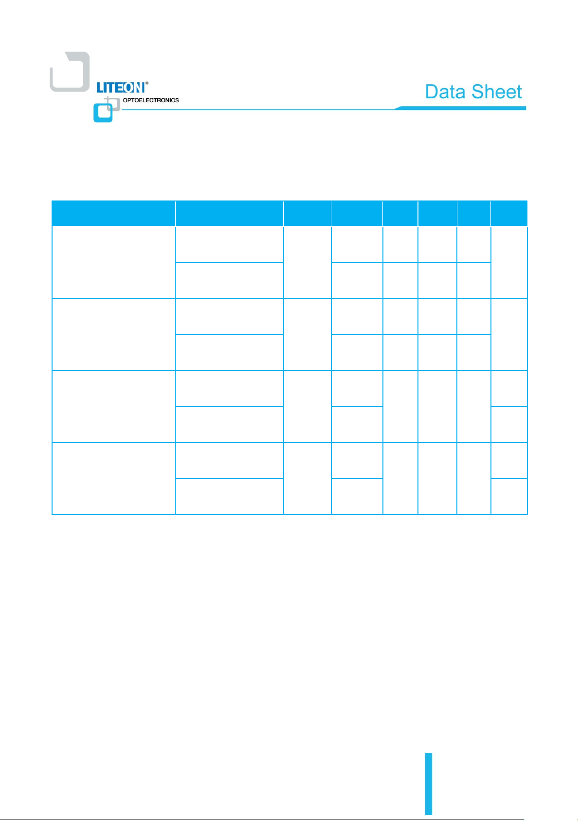
5. SWITCHING SPECIFICATION
Parameter
Test Condition
Symbol
Device
Min
Typ
Max
Units
Propagation Delay Time to
Low Output Level
TA=25℃
(R
L
=4.1KΩ, I
F
=16mA)
t
PHL
6N135
-
0.09
1.5
μs
TA=25℃
(R
L
=1.9KΩ, I
F
=16mA)
6N136
-
0.1
0.8
Propagation Delay Time to
High Output Level
TA=25℃
(R
L
=4.1KΩ, I
F
=16mA)
t
PLH
6N135
-
0.8
1.5
μs
TA=25℃
(R
L
=1.9KΩ, I
F
=16mA)
6N136
-
0.4
0.8
Logic High Common Mode
Transient Immunity
IF=0mA;VCM=10Vp-p;
R
L
=4.1KΩ; T
A
=25C
|CMH|
6N135
1
10
-
KV/μs
IF=0mA;VCM=10Vp-p;
R
L
=1.9KΩ; T
A
=25C
6N136
KV/μs
Logic Low Common Mode
Transient Immunity
IF=0mA;VCM=10Vp-p;
R
L
=4.1KΩ; T
A
=25C
|CML|
6N135
1
10
-
KV/μs
IF=0mA;VCM=10Vp-p;
R
L
=1.9KΩ; T
A
=25C
6N136
KV/μs
* TA=0~70℃, Vcc=5V, unless otherwise specified.
* All Typical at TA =25oC
7/15
Page 9
Photocoupler
6N135-L 6N136-L series
Part No. : 6N135-L 6N136-L series
BNS-OD-FC002/A4
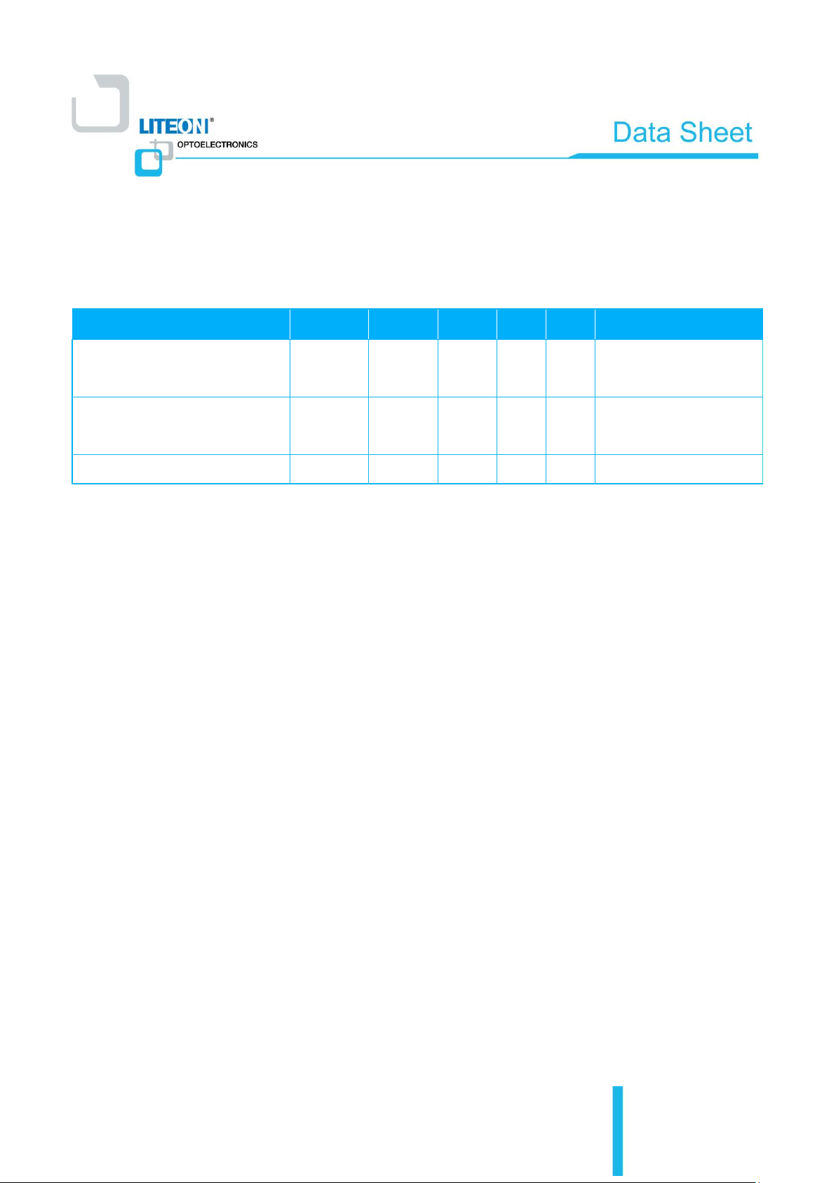
6. ISOLATION CHARACTERISTIC
Parameter
Symbol
Min.
Typ.
Max.
Unit
Test Condition
Input-Output Insulation Leakage
Current
I
I-O
— —
1.0
μA
45% RH, t = 5s,
V
I-O
= 3kV DC, TA =25oC
Withstand Insulation Test Voltage
V
ISO
5000
— — V
RMS
RH ≤ 50%, t = 1min,
TA = 25oC
Input-Output Resistance
R
I-O
—
1012 — Ω
V
I-O
= 500V DC
*All Typical at T
A
=25oC
Notes
1. A 0.1µF or bigger bypass capacitor for VCC is needed as shown in Fig.1
2. Current Transfer Ratio is defined as the ratio of output collector current Io , to the forward LED input current IF, times 100.
3. The 1.9KΩ load represents 1TTL unit load of 1.6mA and the 5.6KΩ pull-up resistor.
4. The 4.1KΩ load represents 1LSTTL unit load of 0.36mA and the 6.1KΩ pull-up resistor.
8/15
Page 10
Photocoupler
6N135-L 6N136-L series
Part No. : 6N135-L 6N136-L series
BNS-OD-FC002/A4
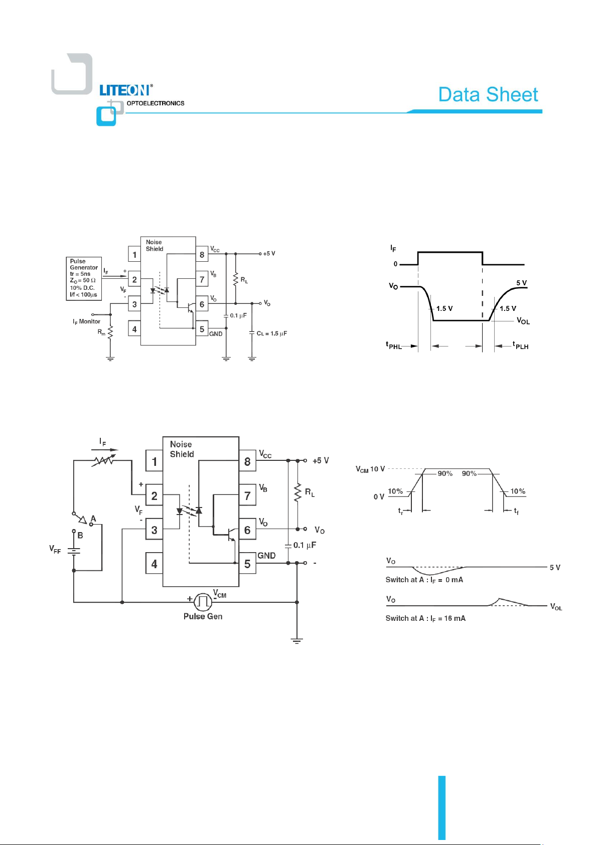
7. SWITCHING TIME TEST CIRCUIT
Figure 1: Test Circuit for t
PHL
and t
PLH
Figure 2: Single Channel Test Circuit for Common Mode Transient Immunity
9/15
Page 11
Photocoupler
6N135-L 6N136-L series
Part No. : 6N135-L 6N136-L series
BNS-OD-FC002/A4
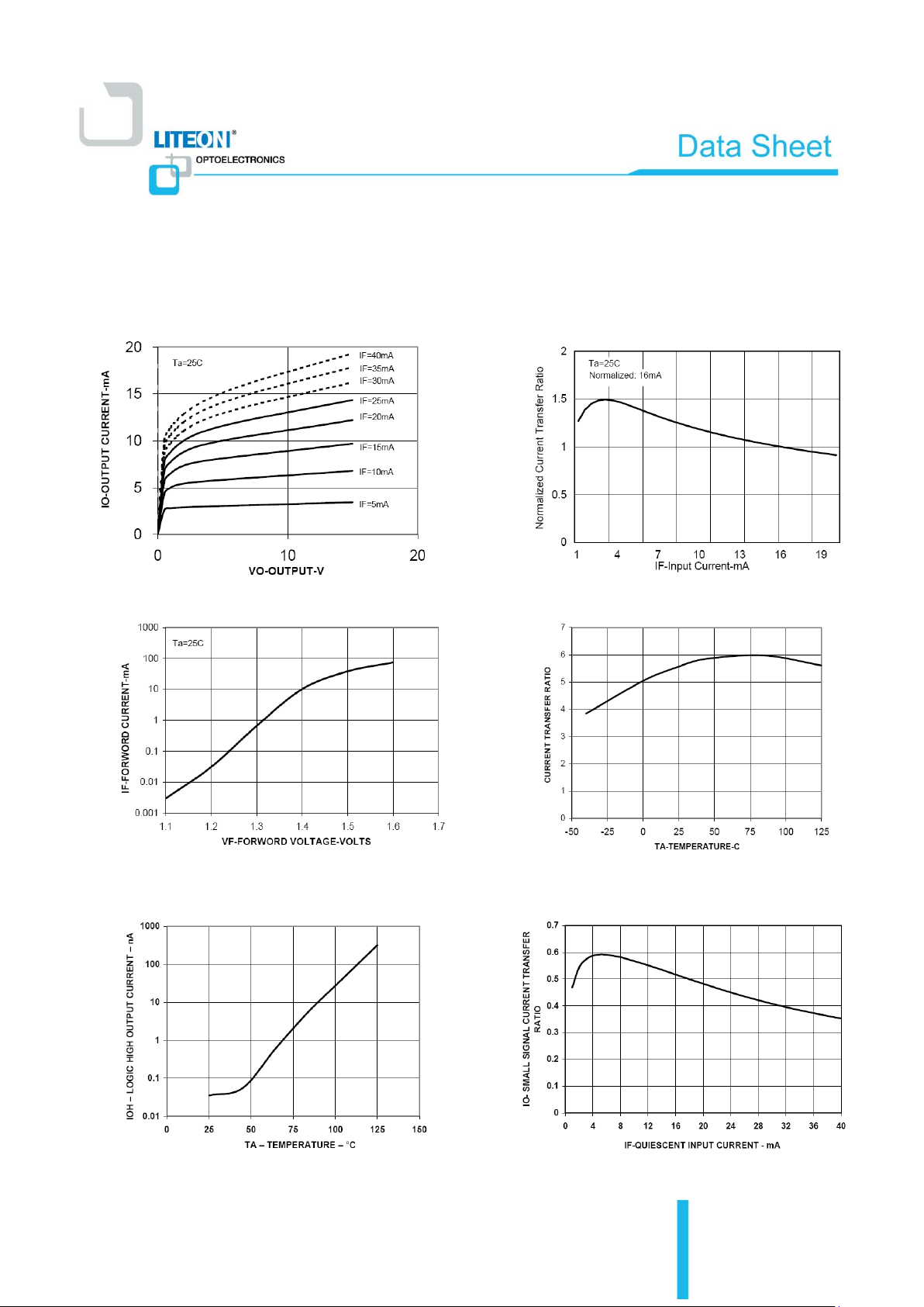
Figure 3: DC and pulsed transfer characteristics
Figure 6: Current transfer ratio vs. input current
Figure 7: Current transfer ratio vs. temperature
Figure 8: Small-signal current transfer ratio vs.
quiescent current
Figure 4: Input current vs. forward voltage
Figure 5: Logic high output current vs. temperature
8. CHARACTERISTIC CURVES
10/15
Page 12
Photocoupler
6N135-L 6N136-L series
Part No. : 6N135-L 6N136-L series
BNS-OD-FC002/A4
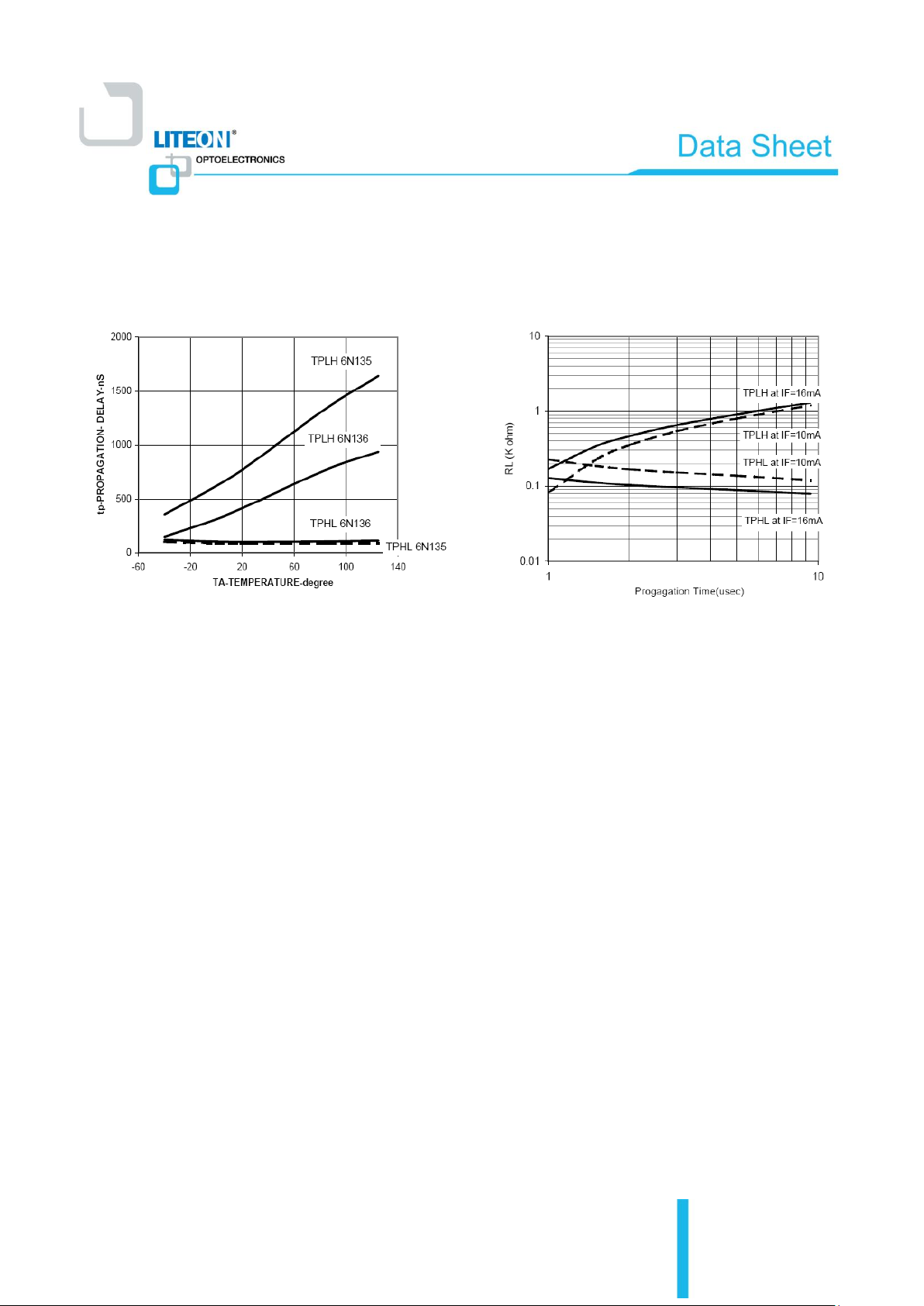
Figure 10: Propagation delay time vs. load resistance
Figure 9: Propagation delay time vs. temperature
11/15
Page 13
Photocoupler
6N135-L 6N136-L series
Part No. : 6N135-L 6N136-L series
BNS-OD-FC002/A4
Profile item
Conditions
Preheat
- Temperature Min (T
Smin
)
- Temperature Max (T
Smax
)
- Time (min to max) (ts)
150˚C
200˚C
90±30 sec
Soldering zone
- Temperature (TL)
- Time (tL)
217˚C
60 ~ 100 sec
Peak Temperature (TP)
260˚C
Ramp-up rate
3˚C / sec max.
Ramp-down rate
3~6˚C / sec
60 ~ 120 sec
25 C
150 C
200 C
260 C
217 C
60-100 sec
Time (sec)
Temperature ( C)
20 sec
Tsmax
ts (Preheat)
tL (Soldering)
Tsmin
TL
TP
Ramp-down
Ramp-up
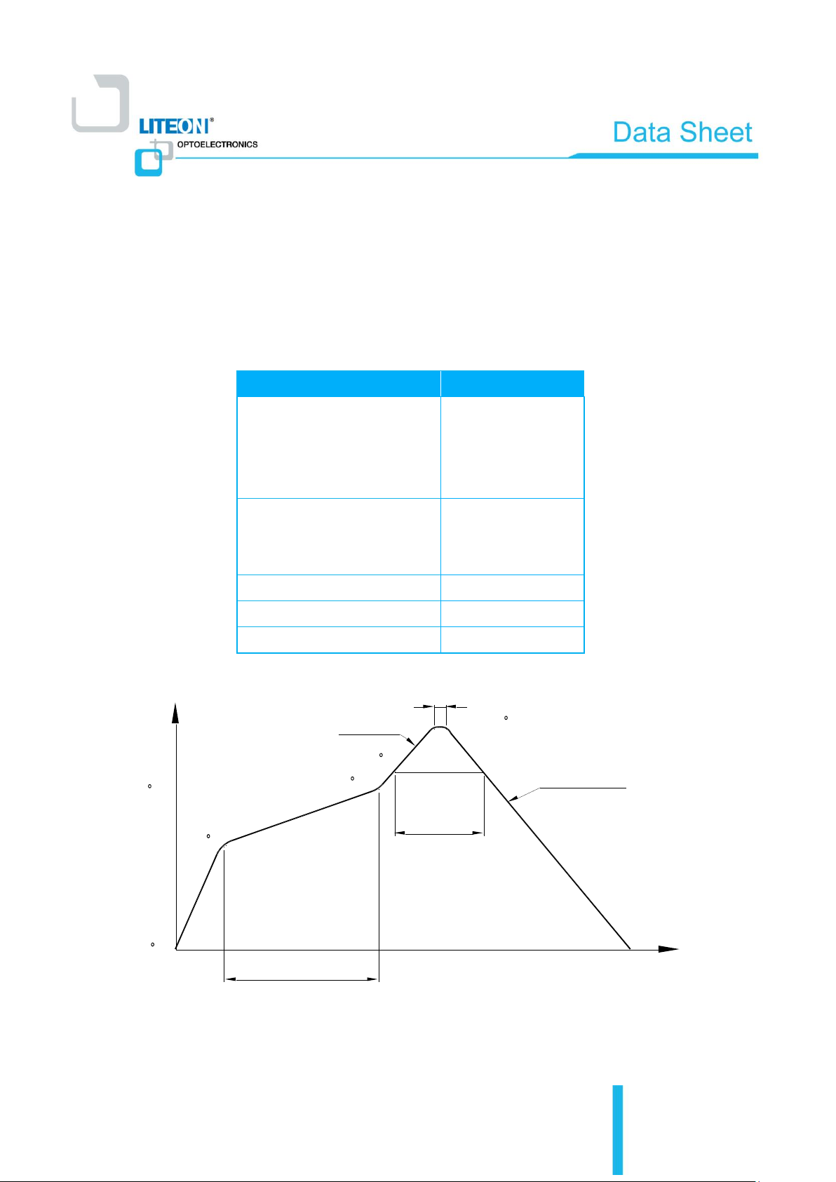
9. TEMPERATURE PROFILE OF SOLDERING
9.1 IR Reflow soldering (JEDEC-STD-020C compliant)
One time soldering reflow is recommended within the condition of temperature and time profile shown below. Do not solder more than three
times.
12/15
Page 14
Photocoupler
6N135-L 6N136-L series
Part No. : 6N135-L 6N136-L series
BNS-OD-FC002/A4
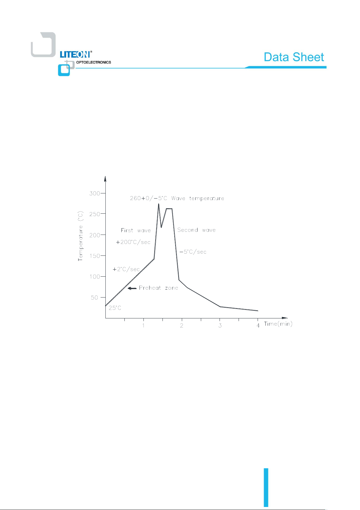
9.2 Wave soldering (JEDEC22A111 compliant)
One time soldering is recommended within the condition of temperature.
Temperature: 260+0/-5˚C
Time: 10 sec.
Preheat temperature:25 to 140˚C
Preheat time: 30 to 80 sec.
9.3 Hand soldering by soldering iron
Allow single lead soldering in every single process. One time soldering is recommended.
Temperature: 380+0/-5˚C
Time: 3 sec max.
13/15
Page 15
Photocoupler
6N135-L 6N136-L series
Part No. : 6N135-L 6N136-L series
BNS-OD-FC002/A4
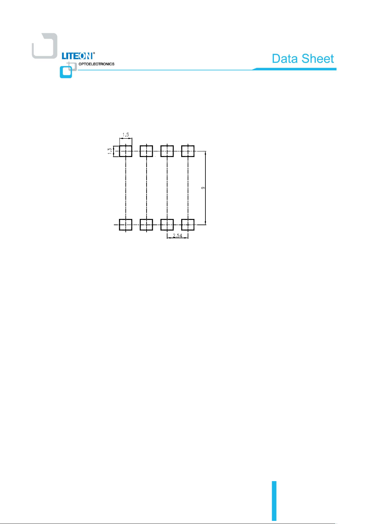
10. RECOMMENDED FOOT PRINT PATTERNS (MOUNT PAD)
Note :
Dimensions in millimeters.
14/15
Page 16
Photocoupler
6N135-L 6N136-L series
Part No. : 6N135-L 6N136-L series
BNS-OD-FC002/A4
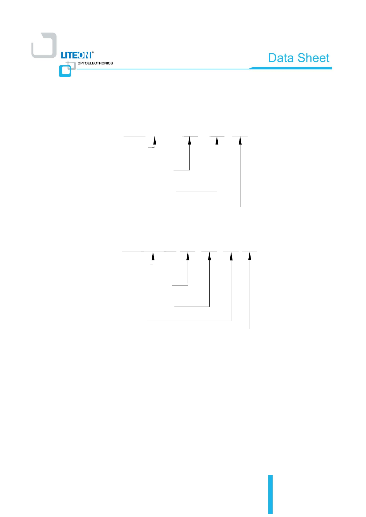
(2) TAPING TYPE (TA, TA1)
Please refer to orientation of taping on Page: P4
(1) No suffix = Dual-in-Line package
M = Wide lead spacing package
S = Surface mounting package
(3) VDE Option
6N13X (1)(2)-V -L
(4) Liteon P/N
DEVICE PART NUMBER
Classified by Electrical Characteristics
Please refer to the table on Page: P6
(2) TAPING TYPE (TA, TA1)
Please refer to orientation of taping on Page: P4
(1) No suffix = Dual-in-Line package
M = Wide lead spacing package
S = Surface mounting package
DEVICE PART NUMBER
Classified by Electrical Characteristics
Please refer to the table on Page: P6
6N13X (1)-(2) -L
(3) Liteon P/N
11. NAMING RULE
Example : 6N135S-TA1-L, 6N136S-TA1-L
Example : 6N135STA1-V-L, 6N136STA1-V-L
12. NOTES
LiteOn is continually improving the quality, reliability, function or design and LiteOn reserves the right to make changes
without further notices.
The products shown in this publication are designed for the general use in electronic applications such as office automation
equipment, communications devices, audio/visual equipment, electrical application and instrumentation.
For equipment/devices where high reliability or safety is required, such as space applications, nuclear power control
equipment, medical equipment, etc, please contact our sales representatives.
When requiring a device for any ―specific‖ application, please contact our sales in advice.
If there are any questions about the contents of this publication, please contact us at your convenience.
The contents described herein are subject to change without prior notice.
Immerge unit’s body in solder paste is not recommended.
15/15
 Loading...