

Page 1
LITEMAX DLF/DLH1744
Sunlight Readable 17” LED B/L LCD
(1st Edition 6/3/2007 )
All information is subject to change without notice.
Approved by Checked by Prepared by
David Sharline Jacky
LITEMAX Electronics Inc.
8F, No.137, Lane 235, Bau-chiau Rd.,
Shin-dian City, Taipei County, Taiwan R.O.C.
Tel : 886-2-8919-1858
Fax: 886-2-8919-1300
Homepage:
http://www.litemax.com.tw
Page 1
Page 2

Record Revision
Version and Date Page Old Description New Description Remark
Page 2
Page 3

Contents
Record Revision 2
Contents 3
Handling Precautions 4
General Description 5
Display Characteristics 5
Optical Characteristics 6
Optical Test 6
Reliability 6
Test Mode: 6
Functional Block Diagram 8
Absolute Maximum Ratings 9
TFT LCD Module 9
Backlight Unit 9
Absolute Ratings of Environment 9
Electrical characteristics 10
TFT LCD Module 10
Signal Characteristic 12
Pixel Format Image 12
The Input Data Format 12
Signal Description 13
Timing Characteristics 15
Connector & Pin Assignment 18
TFT LCD Module 18
Backlight Unit 19
Reliability Test 20
LED Backlight Dimming & Power Consumption and Temperature Relationship Test
Report 21
Mechanical Characteristics 23
Page 3
Page 4

Handling Precautions
1) Since front polarizer is easily damaged, be extremely careful when handling panel.
2) Be sure to turn off power supply when inserting or disconnecting from input
connectors.
3) Wipe off water immediately. Long contact with water may cause discoloration or spots.
4) When the panel surface is soiled, wipe it with absorbent cotton or other soft cloth.
5) Since the panel is made of glass, it may break or crack if dropped or bumped on a
hard surface.
6) Since CMOS LSI is used in this module, be careful of static electricity by grounding
those handling the display.
7) Do not open nor modify the module assembly.
8) Do not press or touch the panel surface with hands or tools.
9) Do not press or move the reflector sheet at the back of the module in any direction.
10) **At the insertion or removal of the signal Interface Connector, be sure not to rotate
nor tilt the interface connector of the TFT module.
11) After installation of the TFT module into an enclosure (Desktop monitor Bezel, for
example), do not twist nor bend the TFT Module even momentarily. Design the
enclosure so that no bending/twisting forces are applied to the TFT module. Otherwise
the TFT module may be damaged.
Page 4
Page 5
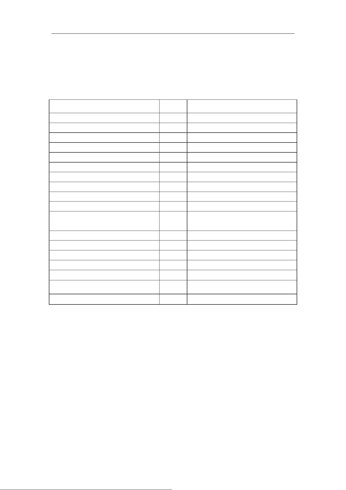
General Description
This specification applies to the 17 inch Color TFT-LCD Module M170EG01 VD.
The display supports the WSXGA+ (1280(H) x 1024(V)) screen format and 16.7M colors
(RGB 6-bits+Hi-RFC data).All input signals are 2 Channel LVDS interface compatible.
This module does not contain an LED driving board for backlight.
Display Characteristics
The following items are characteristics summary on the table under 25 ℃condition:
Items Unit Specifications
Screen Diagonal [mm] 432 (17.0”)
Active Area [mm] 337.920(H) ×270.336(V)
Pixel Pitch [mm] 0.264(per one triad) ×0.264
[cd/m
Optical ResponseTime [msec] 5 (Typ)
Nominal Input Voltage VDD [Volt] +5.0 (Typ)
2]
1280 × 3(RGB) ×1024 Pixels H x V
R.G.B. Vertical Stripe Pixel Arrangement
Normally White Display Mode
1000 (center,Typ) White Luminance
1000 : 1 (Typ) Contrast Ratio
Power Consumption [Watt] 34.5W (Typ) (PDD=6W, PBL=28.5W )
Weight [Grams] 2120
Physical Size (H x V x D)
Support Color
Temperature Range Operating Storage
(Non-Operating)
RoHS Compliance RoHS Compliance
[mm]
oC] [oC]
358.5*296.5*15.8
Dual Channel LVDS Electrical Interface
Anti-glare type, Hardness 3H Surface Treatment
16.7M colors (RGB 6-bits + FRC data)
0 to +50
-20 to + 60 [
Page 5
Page 6
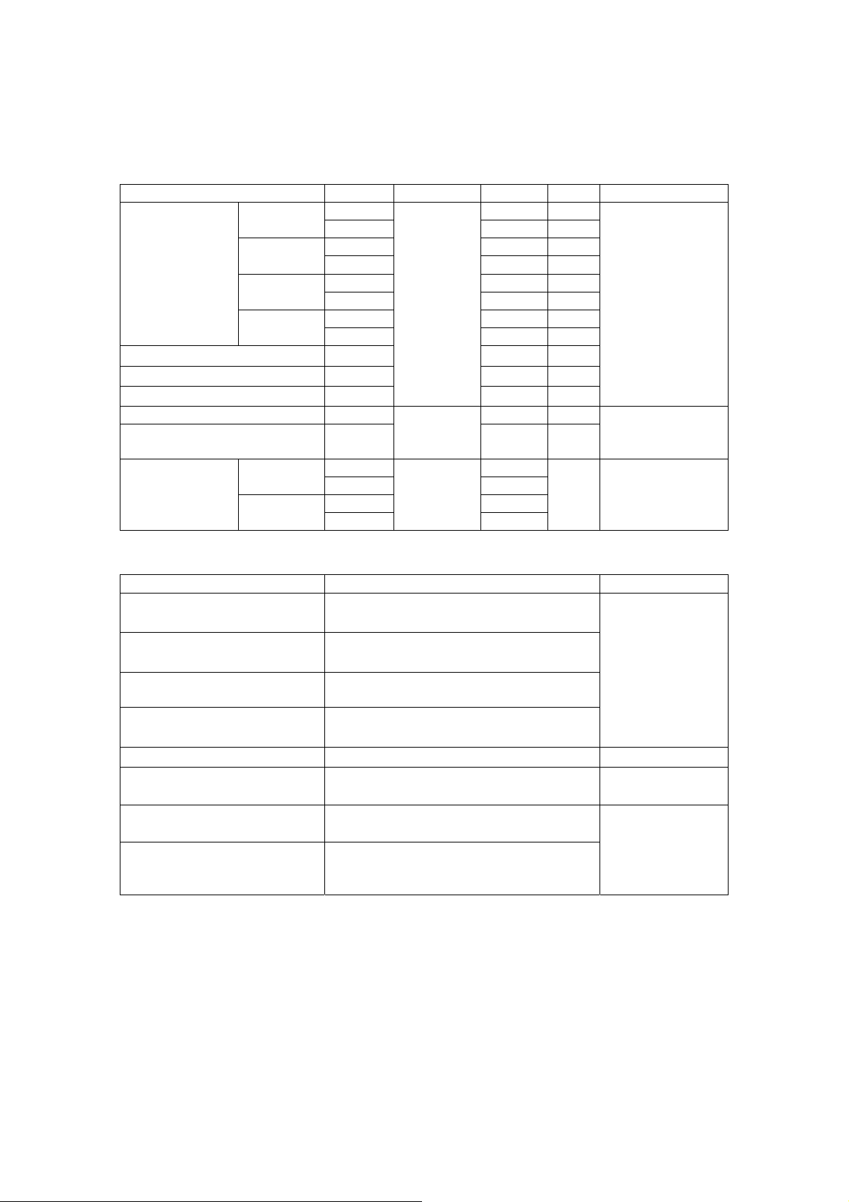
Optical Characteristics
The optical characteristics are measured under stable conditions at 25℃(Room Temperature):
Optical Test
Optical
Item Symbol Condition Data Unit Note
Red
Color
chromaticity
Center Luminance of White Lc 1060
Average La 880
Uniform Lu
Contrast Ratio CR 1000 -
Color Saturation 75
Viewing Angle
Green
Blue
White
Horizontal
Vertical
Rx 0.6386 Ry 0.3548 Gx 0.3356 Gy 0.598 Bx 0.1438 -
By 0.0724 Wx 0.3236 Wy 0.3533 -
NTSC
θx+ 80
θx- 80
θy+ 80
θy- 80
θx=0
θy=0
BM-7
θx=0
θy=0
Klein K-10
CR≧10
76
cd/㎡
cd/㎡
%
%
Deg
Test Mode:
(1)(2)(3)
Test Mode:
(1)(4)
Test Mode:
(1)(3)
Reliability
Item Fill the Bill Note
torage Temperature
Operating Temperature
High Temperature &
Humidity
Thermal Shock
Life
Vibration
Shock(white carton)
Drop (white carton)
Test Mode:
Max:60℃
Min:-20℃
Max:50℃
Min:-10℃
50℃,RH 80%,24 hours
-20℃,0.5hour to 60℃,0.5hour
100cycle,1hour/cycle
-----℃--------hours Test Mode(6)
1.5G,10-200-10Hz,30Min
each Axis (X,Y,Z)
50G,20ms ,
Half-sine wave (X,Y,Z)
Height: 60 cm
1corner,3edges,6surfaces
(ASTMD4169-I)
Time:24hours
Time:24hours
Time:24hours
Time:24hours
Test Mode:(5)
Test Mode:(7)
Test Mode:(7)
(1) (θx,θy)/Definition of Viewing Angle(θx,θy):
Page 6
Page 7
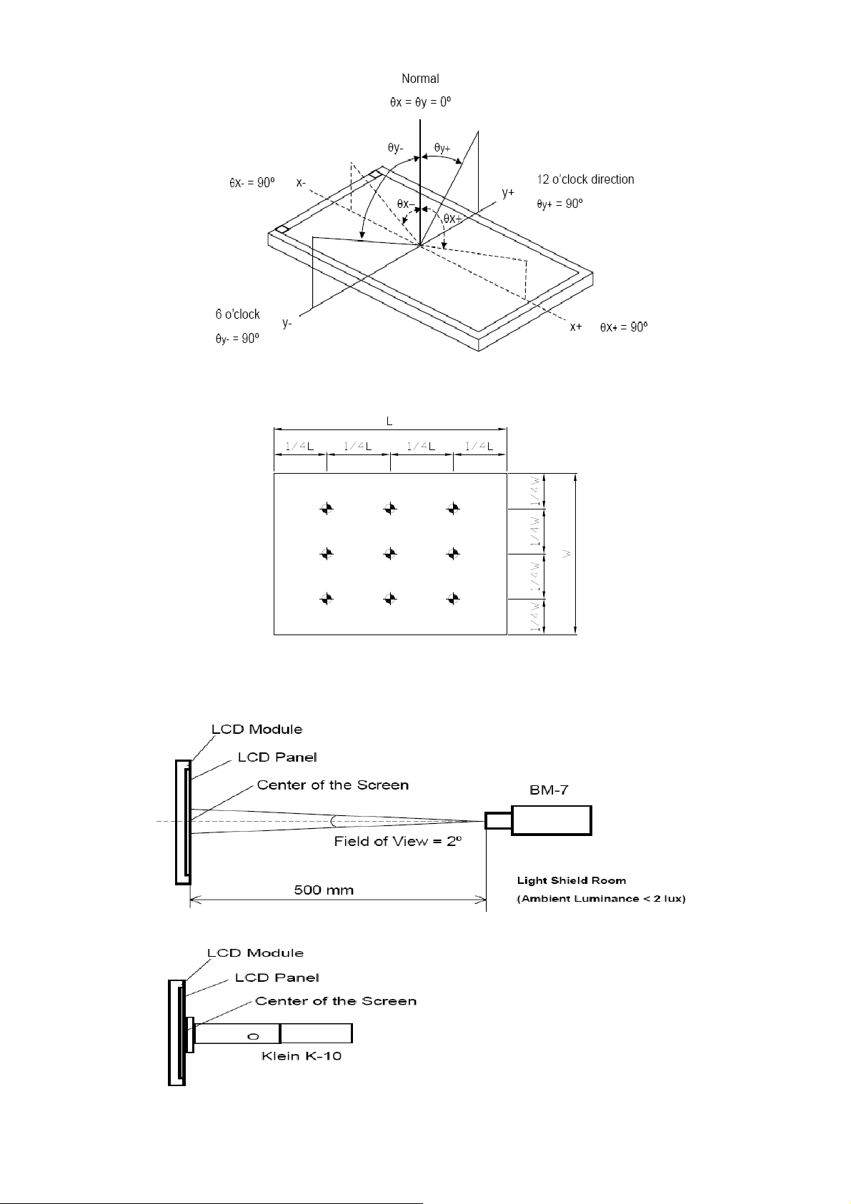
(2) Definition of Test Point:
1
2
3
BA C
Active Area
(3)BM-7 Measurement Setup:
(4)Klein K-10 Measurement Setup:
Page 7
Page 8
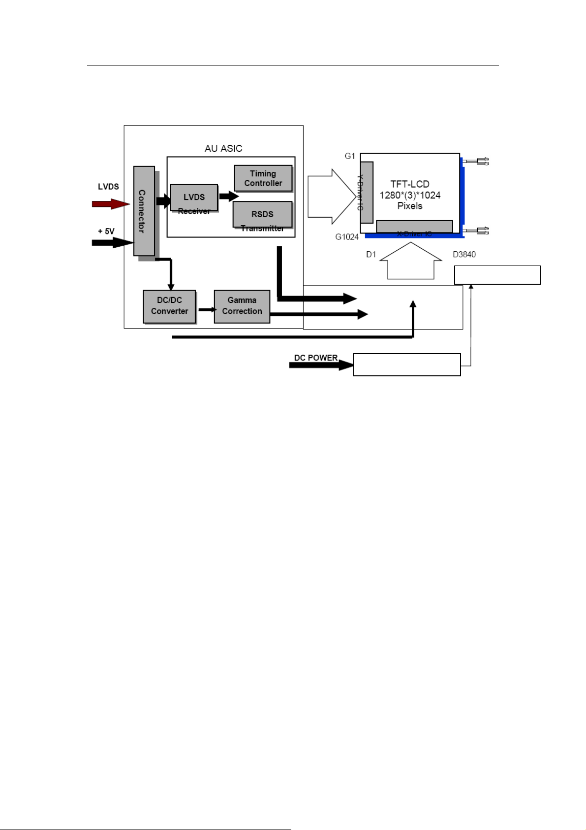
Functional Block Diagram
The following diagram shows the functional block of the 17.0 inches Color TFT-LCD
Module:
LLL
LED Bar Line
LED Driving Board
Page 8
Page 9
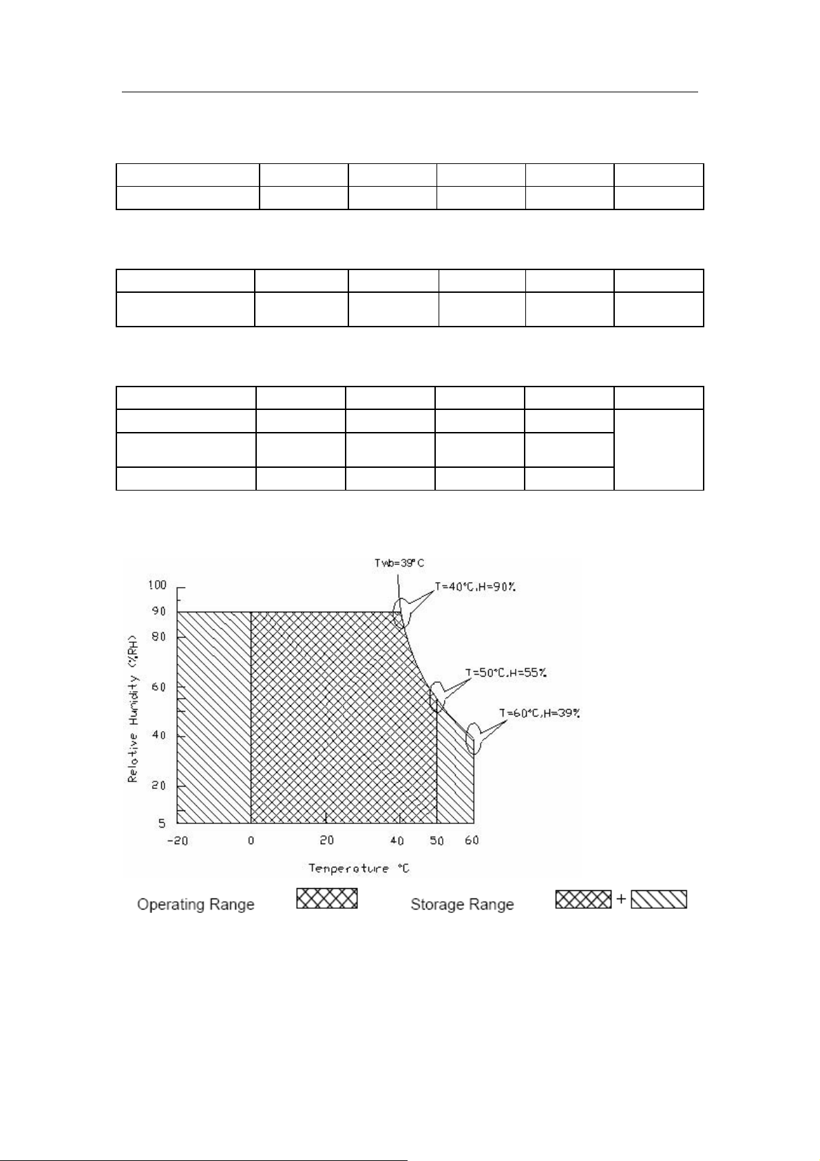
Absolute Maximum Ratings
Absolute maximum ratings of the module are as following:
TFT LCD Module
Item Symbol Min Max Unit Conditions
Logic/LCD Drive VIN -0.3 6 [Volt] Note 1,2
Backlight Unit
Item
LED Light bar
Current
Symbol Min Max Unit Conditions
I
LED
-
800 [mA] rms Note 1,2
Absolute Ratings of Environment
Item Symbol Min Max Unit Conditions
Operating Humidity HOP 5 90 [%RH]
Storage
Temperature
TST -20 +60 [
Storage Humidity HST
oC]
5 90 [%RH]
Note 3
Note 1: With in Ta (25℃ )Note 2: Permanent damage to the device may occur if exceed
maximum valuesNote 3:
Inspection Standard).
For quality performance, please refer to AUO IIS (Incoming
Note 2: Permanent damage to the device may occur if exceed maximum values
Note 3:
Standard).
For quality performance, please refer to LiteMax IIS (Incoming Inspection
Page 9
Page 10
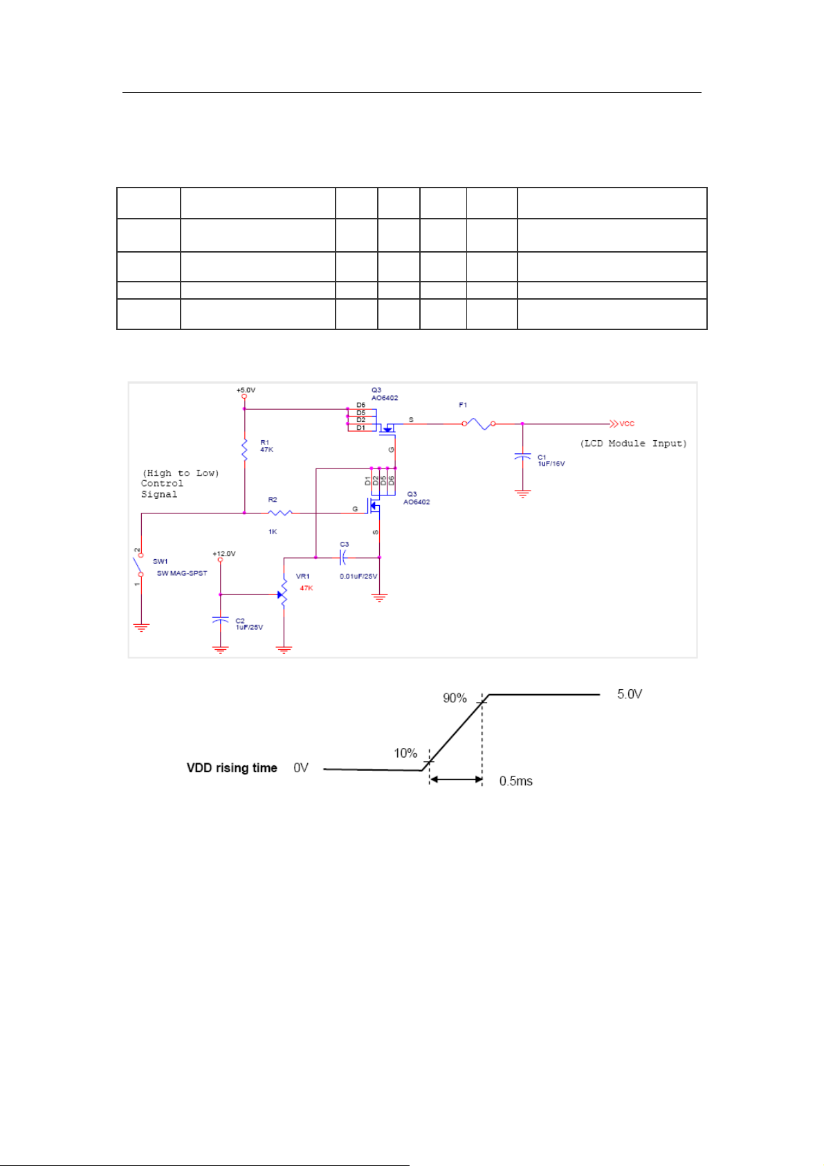
Electrical characteristics
TFT LCD Module
Power Specification
Input power specifications are as follows:
Symble Parameter Min. Typ. Max. Unit Condition
VCC
ICC Input Current - 1.2 1.56 [A]
IRush Inrush Current - - 3.0 [A] Note
PCC VCCPower - 6
Logic/LCD Drive
Voltage
4.5 5.0 5.5 [Volt]
7.8 [Watt]
±10%
Vin=5V , All Black Pattern, at
75Hz
Vin=5V , All Black Pattern, at
75Hz
Note: Measurement conditions:
Page 10
Page 11
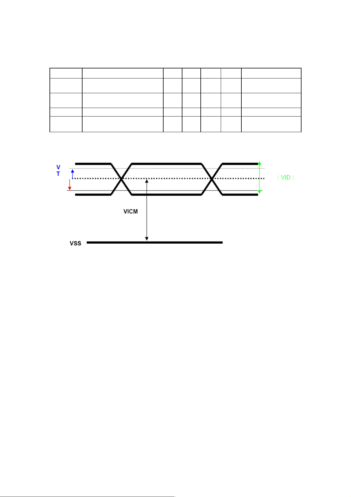
Signal Electrical Characteristics
Input signals shall be low or Hi-Z state when Vin is off It is recommended to refer the
specifications of SN75LVDS82DGG (Texas Instruments) in detail.
Each signal characteristics are as follows;
Symbol Parameter Min Typ Max Units Condition
VTH
VTL
│VID│
VICM
Differential Input High
Threshold
Differential Input Low
Threshold
- - +100 [mV]
-100 - - [mV]
Input Differential Voltage 100 400 600 [mV] Note
Differential Input Common
Mode Voltage
+1.0 +1.2
+1.5 [V]
VICM = 1.2V Note
VICM = 1.2V Note
VTH/VTL = ±
100MV Note
Note: LVDS Signal Waveform
Page 11
Page 12
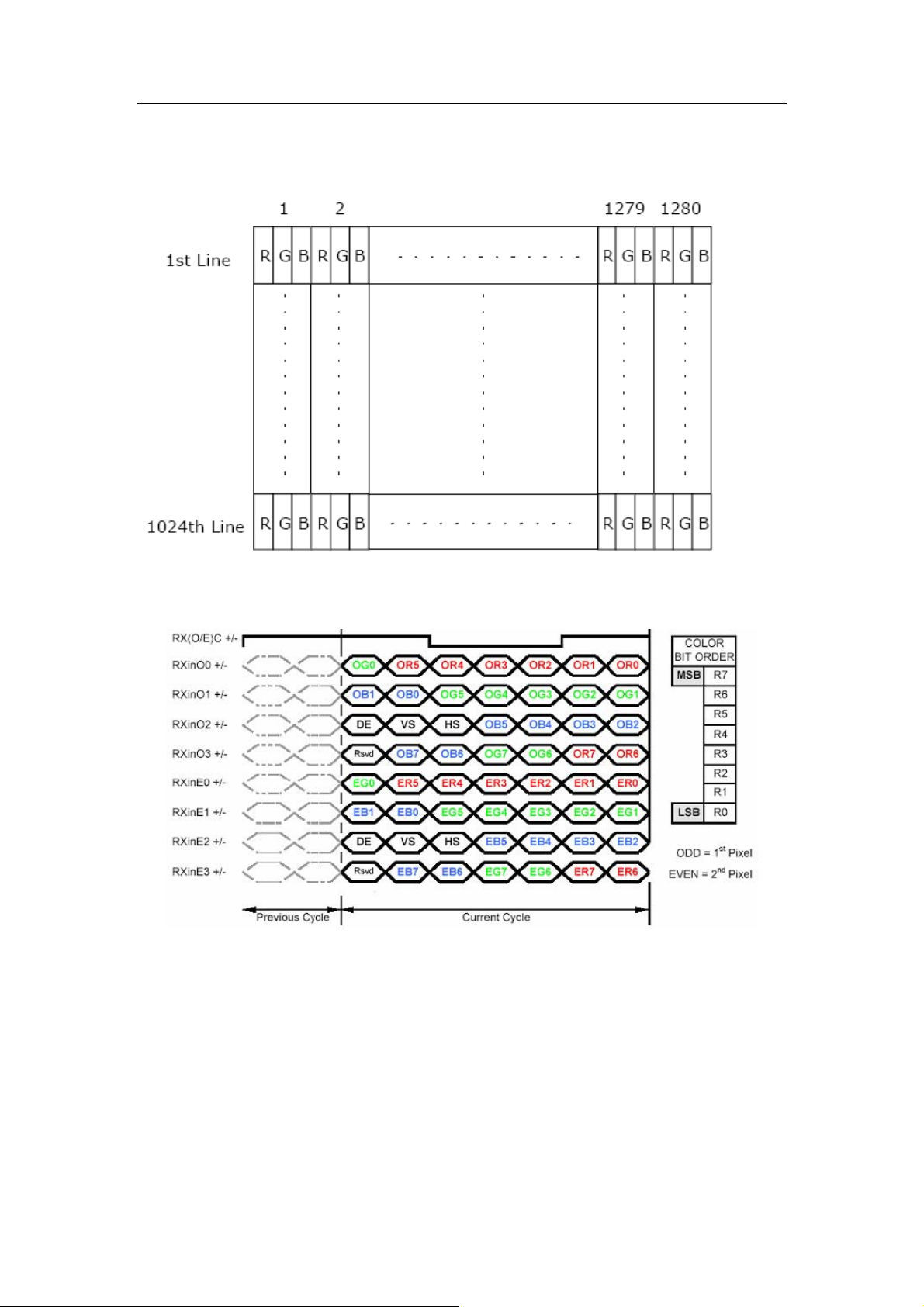
Signal Characteristic
Pixel Format Image
Following figure shows the relationship of the input signals and LCD pixel format.
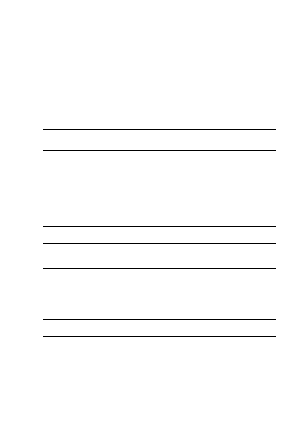
The Input Data Format
Note1: Normally, DE, VS, HS on EVEN channel are not used.
Note2: Please follow PSWG.
Note3: 8-bit in
Page 12
Page 13
Signal Description
The module using a pair of LVDS receiver SN75LVDS82(Texas Instruments) or
compatible. LVDS is a differential signal technology for LCD interface and high speed data
transfer device. Transmitter shall be SN75LVDS83 (negative edge sampling) or
compatible. The first LVDS port (RxOxxx) transmits odd pixels while the second LVDS port
(RxExxx) transmits even pixels.
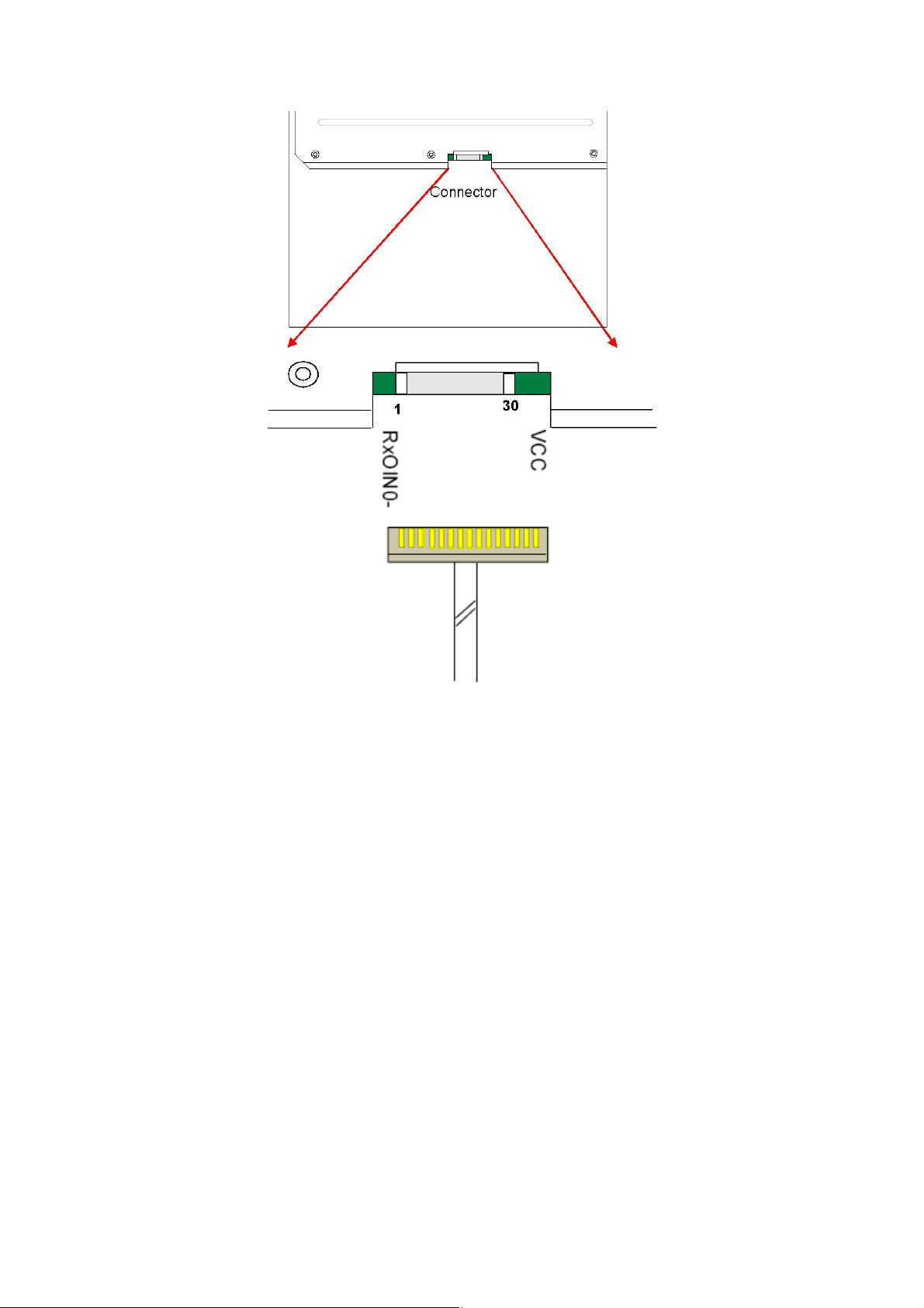
PIN # SIGNAL NAME DESCRIPTION
1 RxO0 Negative LVDS differential data input (Odd data)
2 RxO0+ Positive LVDS differential data input (Odd data)
3 RxO1 Negative LVDS differential data input (Odd data)
4 RxO1+ Positive LVDS differential data input (Odd data)
RxO2
6
7 GND Power Ground
8 RxOC- Negative LVDS differential clock input (Odd clock)
9 RxOC+ Positive LVDS differential clock input (Odd clock)
11 RxO3+ Positive LVDS differential data input (Odd data)
12 RxE0 Negative LVDS differential data input (Even clock)
13 RxE0+ Positive LVDS differential data input (Even data)
14 GND Power Ground
16 RxE1+ Negative LVDS differential data input (Even data)
17 GND Power Ground
18 RxE2 Negative LVDS differential data input (Even data)
19 RxE2+ Positive LVDS differential data input (Even data)
21 RxEC+ Positive LVDS differential clock input (Even clock)
22 RxE3 Negative LVDS differential data input (Even data)
23 RxE3+ Positive LVDS differential data input (Even data)
24 GND Power Ground
26 NC No contact (For AUO test only)
27 GND Power Ground
28 VCC +5.0V Power Supply
29 VCC +5.0V Power Supply
30 VCC +5.0V Power Supply
RxO2+
RxO3 Negative LVDS differential data input (Odd data)
RxE1 Positive LVDS differential data input (Even data)
RxEC- Negative LVDS differential clock input (Even clock)
GND Power Ground
Negative LVDS differential data input (Odd data,
H-Sync,V-Sync,DSPTMG)
Positive LVDS differential data input (Odd data,
H-Sync,V-Sync,DSPTMG)
Page 13
Page 14
Note1: Start from left side
Note2: Input signals of odd and even clock shall be the same timing. Note3: Please follow
PSWG.
Page 14
Page 15
Timing Characteristics
Basically, interface timings described here is not actual input timing of LCD module but
output timing of SN75LVDS82DGG (Texas Instruments) or equivalent.
Signal Item Symbol Min Typ Max Unit
Period Tv 1032 1066 2048 Th
Vertical Section
Horizontal Section
Clock
Frame rate Frame rate F 49 60 76 Hz
Note : DE mode only
Active Tdisp(v) 1024 1024 1024 Th
Blanking Tbp(v)+Tfp(v)+PWvs 8 42 1024 Th
Period Th 680 844 2048 Tclk
Active Tdisp(h) 640 640 640 Tclk
Blanking Tbp(h)+Tfp(h)+PWhs 40 204 1408 Tclk
Period Tclk 14.81 18.52 - ns
Frequency Freq 40 54 70 MHz
Page 15
Page 16
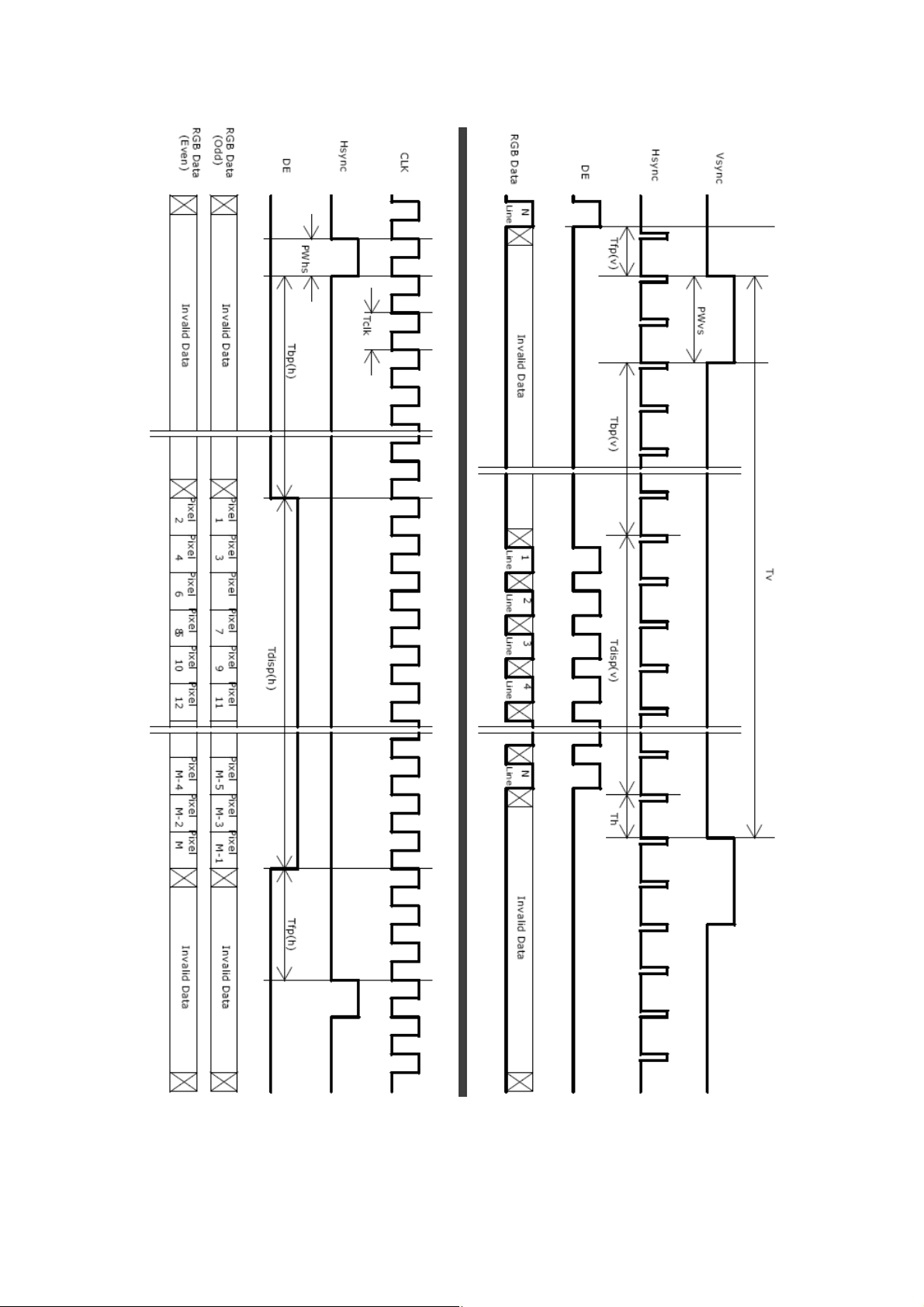
Timing Diagram
Page 16
Page 17
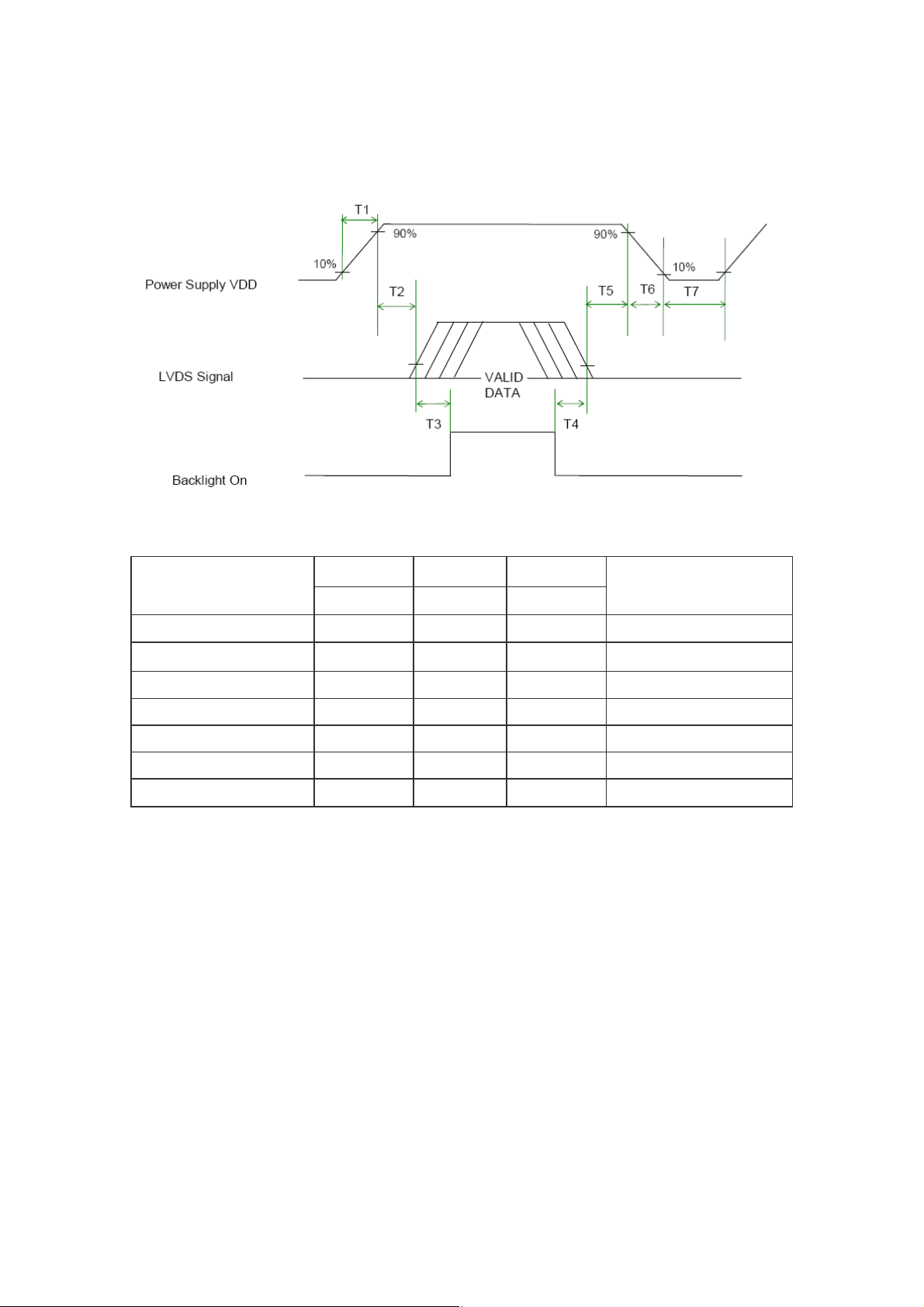
Power ON/OFF Sequence
VDD power and lamp on/off sequence is as follows. Interface signals are also shown in the
chart. Signals from any system shall be Hi-Z state or low level when VDD is off.
Power Sequence Timing
Parameter
Value
Unit
Min. Typ. Max.
T1 0.5 - 10 [ms]
T2 0 - 10 [ms]
T3 200 - - [ms]
T4 100 - - [ms]
T5 0 16 50 [ms]
T6 - - 10 [ms]
T7 1000 - - [ms]
Note: The values of the table are following PSWG.
Page 17
Page 18
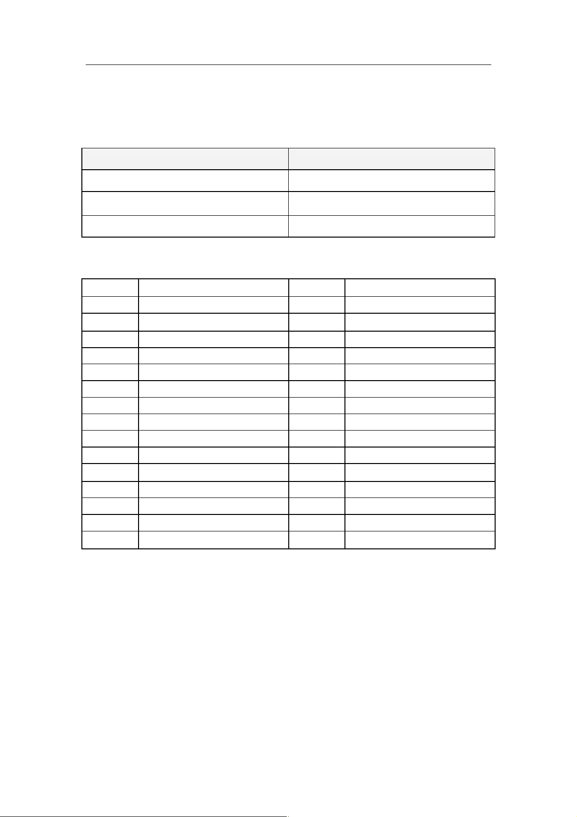
Connector & Pin Assignment
Physical interface is described as for the connector on module. These connectors are
capable of accommodating the following signals and will be following components
TFT LCD Module
Connector
Connector Name / Designation Interface Connector / Interface card
Manufacturer JAE / Hirose or compatible
.
Type Part Number
FI-XB30SSL-HF15 /
MDF76TW-30S-1H(58)
Mating Housing Part Number JAE FI-X30HL
Pin Assignment
Pin# Signal Name Pin# Signal Name
1 RxOIN0 2 RxOIN0+
3 RxOIN1 4 RxOIN1+
5 RxOIN2 6 RxOIN2+
7
9 RxOCLKIN+ 10 RxOIN3-
11 RxOIN3+ 12 RxEIN0-
13 RxEIN0+ 14
15 RxEIN1 16 RxEIN1+
17
19 RxEIN2+ 20 RxECLKIN-
21 RxECLKIN+ 22 RxEIN3-
GND
GND
8 RxOCLKIN-
GND
18 RxEIN2-
23 RxEIN3+ 24
25 NC 26 NC
27 NC 28 VCC
29 VCC 30 VCC
GND
Page 18
Page 19
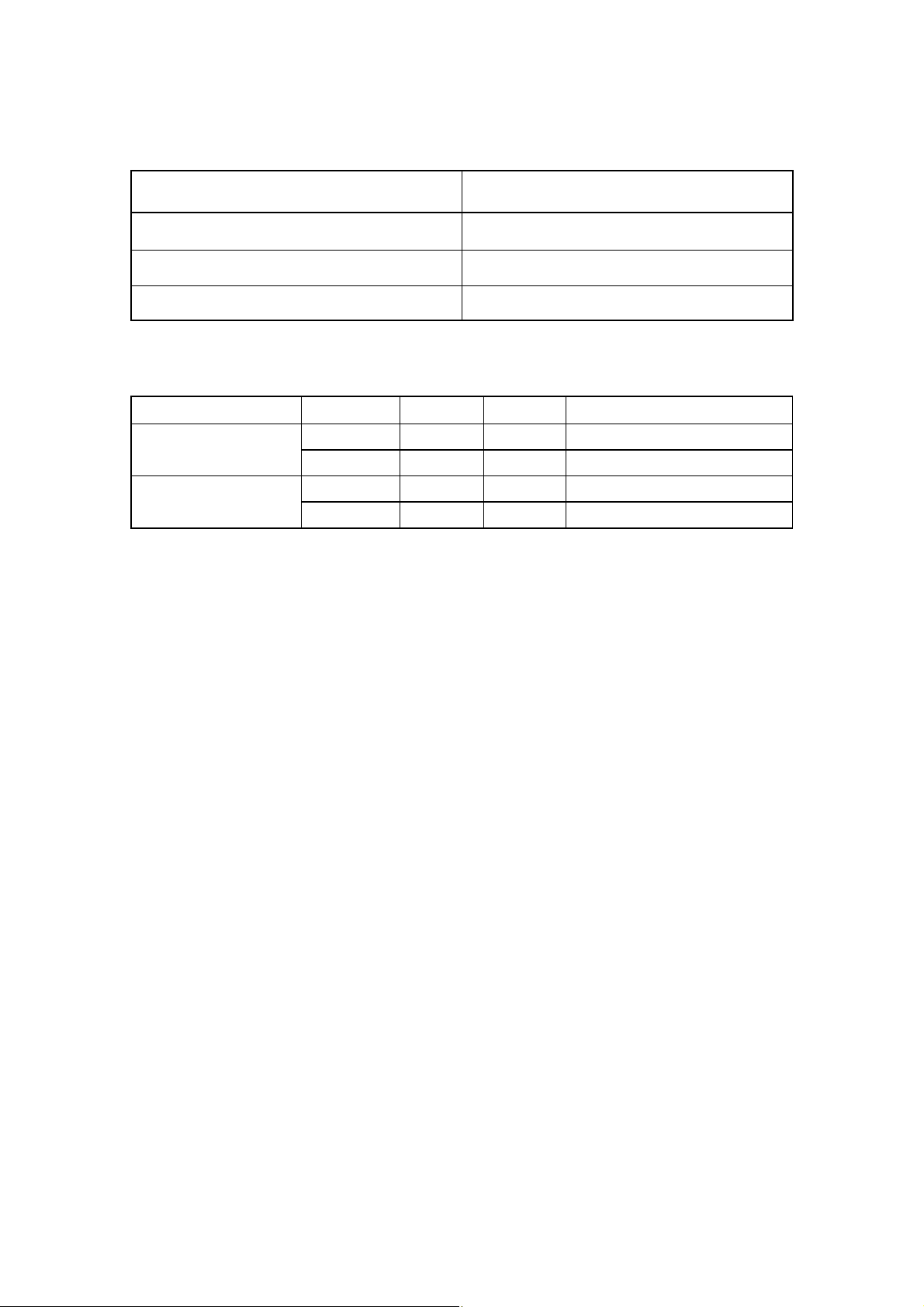
Backlight Unit
Physical interface is described as for the connector on module. These connectors are
capable of accommodating the following signals and will be following components.
Connector Name / Designation Lamp Connector / Backlight lamp
Manufacturer JST
Type Part Number
Mating Type Part Number
EHR-2 or Compatible
S2B-EH or Compatible
Signal for LED Backlight connector
Connector No. Pin No. Input Color Function
CN1
CN2
1 Vcc RED
2 Gnd Black
1
2 Gnd Black
Vcc RED
Positive pole
Negative pole
Positive pole
Negative pole
Page 19
Page 20
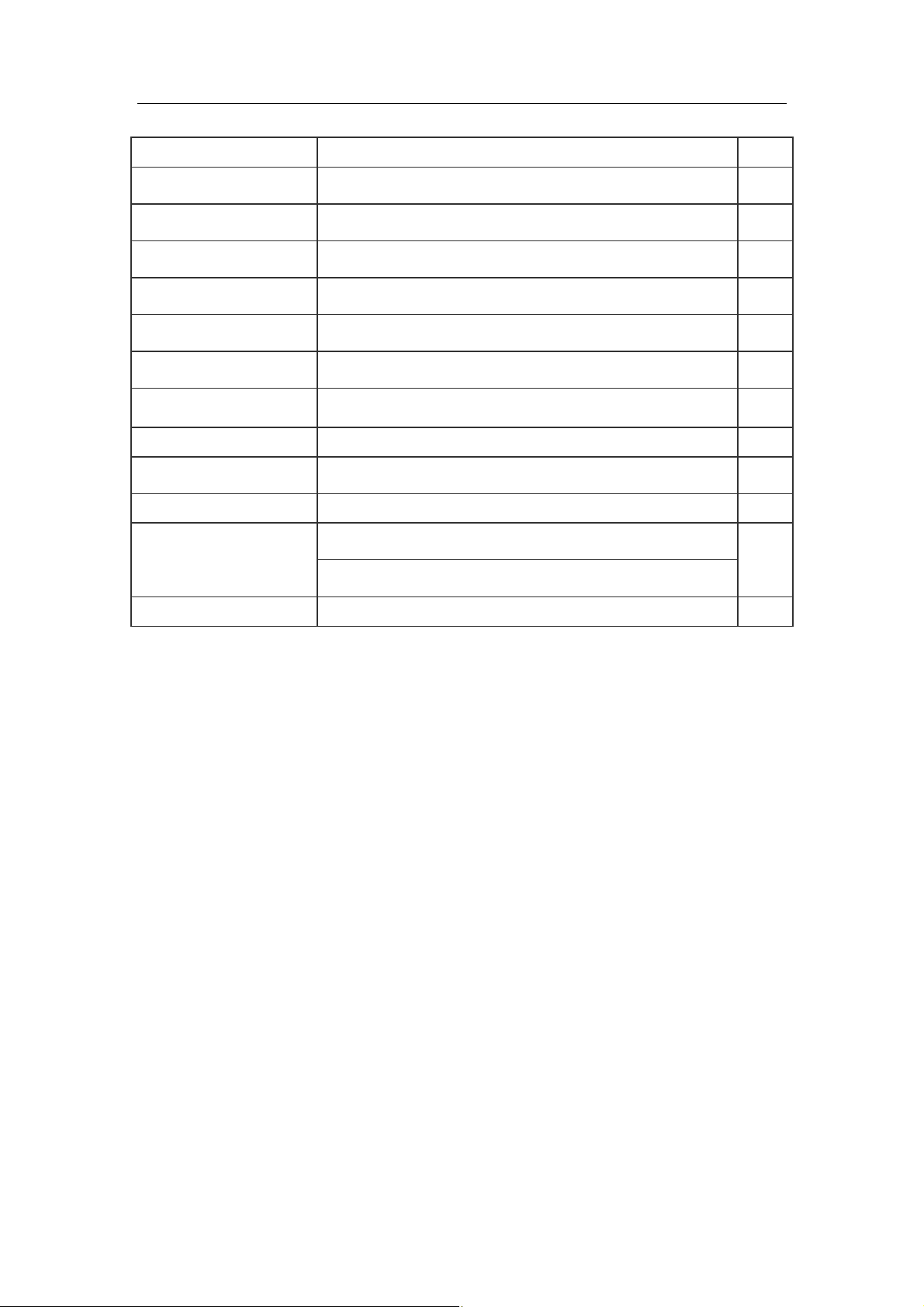
Reliability Test
Environment test conditions are listed as following table.
Items
Temperature Humidity
Bias (THB)
High Temperature
Operation (HTO)
Low Temperature
Operation (LTO)
High Temperature
Storage (HTS)
Low Temperature
Storage (LTS)
Vibration Test
(Non-operation)
Shock Test
(Non-operation)
Drop Test
Thermal Shock Test
(TST)
On/Off Test
ESD (ElectroStatic
Discharge)
Altitude Test Operation:10,000 ft Non-Operation:30,000 ft
Required Condition
Ta= 50 ℃, 80%RH, 300hours
Ta= 50 ℃, 50%RH, 300hours
Ta= 0℃, 300hours
Ta= 60 ℃, 300hours
Ta= -2 0℃, 300hours
Acceleration: 1.5 G Wave: Random Frequency: 10 - 200
-10 Hz Sweep: 30 Minutes each Axis (X, Y, Z)
Acceleration: 50 G Wave: Half-sine Active Time: 20 ms
Direction: ±X, ±Y, ±Z (one time for each Axis)
Height: 60 cm, package test
-20℃/30min, 60℃/30min, 100 cycles
On/10sec, Off/10sec, 30,000 cycles
Contact Discharge: ±8KV, 150pF(330Ω ) 1sec, 8 points,
25 times/ point.
Air Discharge: ±15KV, 150pF(330Ω ) 1sec 8 points,
25 times/ point.
Note
1
2
Note (1) The TFT-LCD module will not sustain damage after being subjected to 100
cycles of rapid temperature change. A cycle of rapid temperature change
consists of varying the temperature from -20℃to 60℃, and back again. Power is
not applied during the test. After temperature cycling, the unit is placed in normal
room ambient for at least 4 hours before power on.
Note (2) According to EN61000-4-2 , ESD class B: Some performance degradation
allowed. No data lost. Self-recoverable. No hardware failures.
Page 20
Page 21
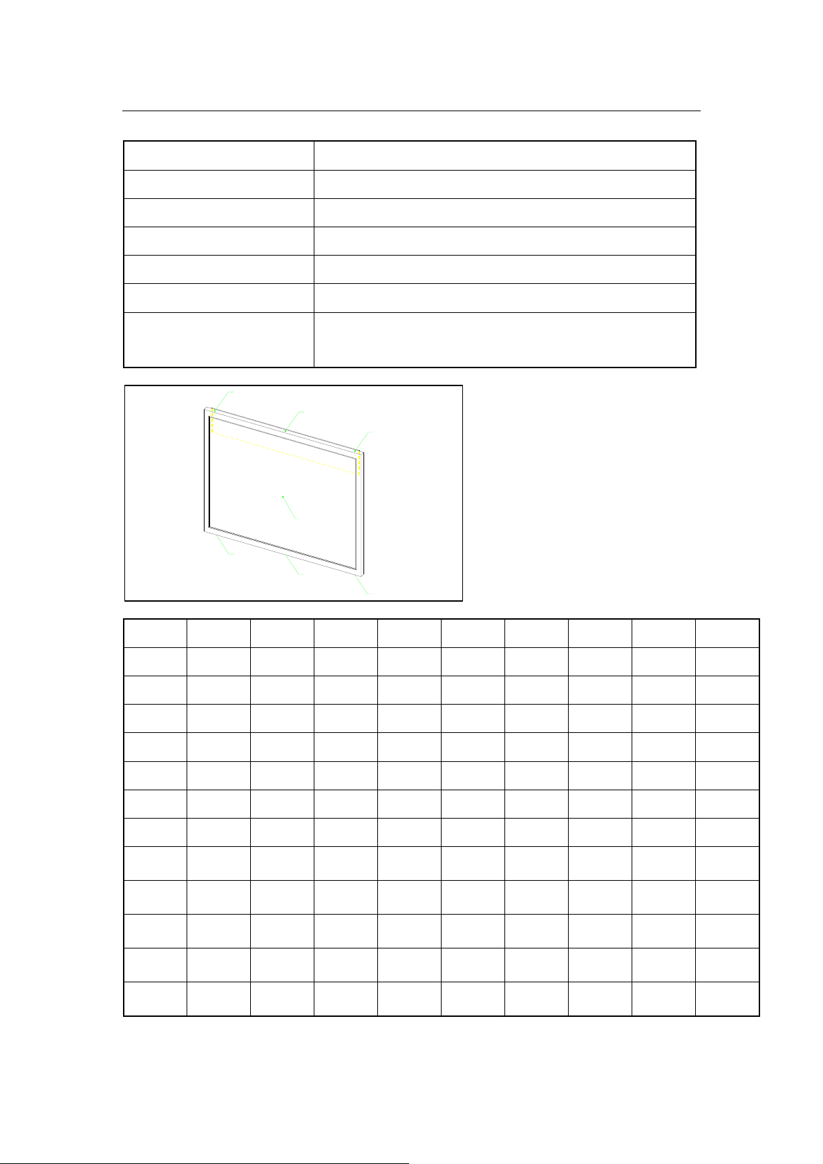
LED Backlight Dimming & Power Consumption and Temperature Relationship Test Report
Test Model AU1744E (M170EG01-VD)
Test Date 2008/4/3
Room Temperature
Test Engineer Jacky_Kuo
A/D Board Model AD5621GA
Brightness & Contrast
Teat Equipment
C
F
25∘C ± 2
B:100% / C:100% / (R、G、B:100%)
DC Power Supply , BM-9 Brightness Meter ,
PT-3S IR Thermal Meter
B
A
Bringtness
Test
Point
E
D
cd/㎡
Vin(V) Iin(A) W Temp A Temp B Temp C
Temp D Temp E Temp F
23 15.2 0.05 0.8 31.2 31.4 31.4 23.6 23.1 23.1
59 15.5 0.1 1.6 32.5 32.9 32.5 23.5 23.7 23.1
109 15.7 0.16 2.5 33.7 34.2 33.2 25.5 24.5 24.2
216 16.1 0.3 4.8 33.8 33.8 33.8 25.6 25.3 25.3
318 16.4 0.43 7.1 37.2 37.8 36.4 28.9 28.6 27.3
417 16.6 0.57 9.5 40.4 40.3 38.9 29.3 28.9 28.3
509 16.8 0.7 11.8 41.3 40.5 39.2 31.4 30.5 28.9
630 17 0.88 15.0 43.4 42.7 42.1 35.7 35.1 33.3
736 17.3 1.05 18.2 44.5 44.5 44.6 37.3 38.5 37
812 17.4 1.2 20.9 47.1 47 47 37 37.1 35.3
910 17.5 1.35 23.6 47 43 41 40 40 37
1030 17.8 1.6 28.5 45.7 47.2 44.4 37.7 37.4 37.8
Page 21
Page 22
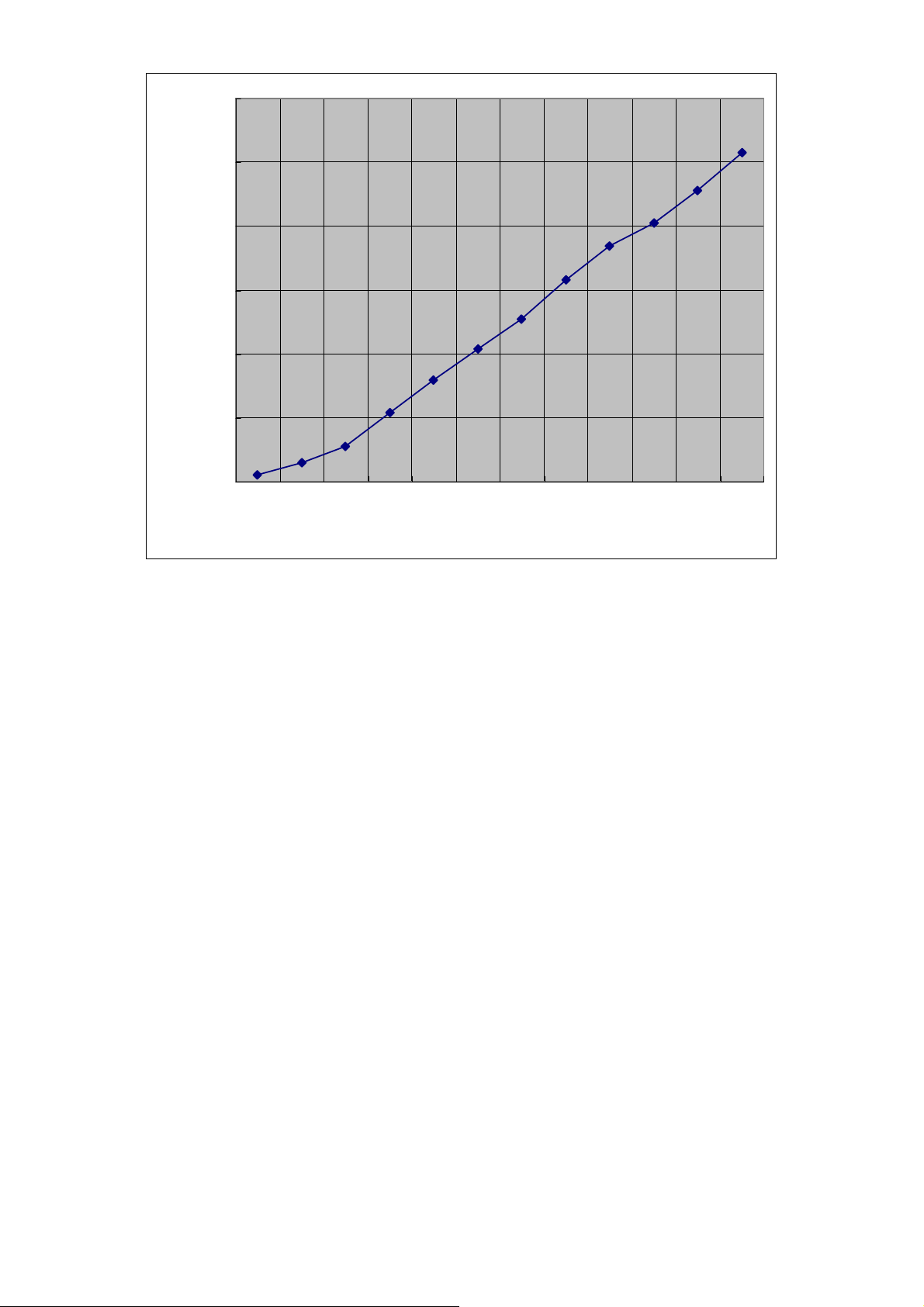
1200
Brightness (cd/m2)
1000
800
600
400
200
812
736
630
509
417
318
216
109
59
0
23
0.8 1.6 2.5 4.8 7.1 9.5 11.8 15.0 18.2 20.9 23.6 28.5
Power Consumption (W)
1030
910
Page 22
Page 23
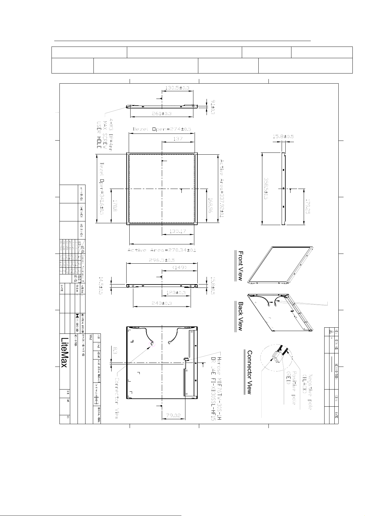
Mechanical Characteristics
Module Size 358.5*296.5*15.8 ㎜
Connector
Part
Jacky_Kuo
JAE FI-XB30SSL(LCD)
JST HER-2 or Compatible(B/L)
CL-X
CL-X
CL-Y
Weight 2120gw
User’s Connector
Part
JAE FI-X30HL(LCD)
JST S2B-EH or Compatible
1.Outline Tolerance:0.5mm
3.Lightbar Cable:U13239 AWG22 L=180± 10m m
Note:
2.Lightbar Connector
:EHR-2 or Compatible
CL-Y
LED Blacklight Power Cable
-
2008.1.21
mm
ASSY_MODULE_AU1744E (M170EG01-VD)
VHB,AUO ,1744,1000nits,V1,M170EG 01,VD,P
LiteMax
Electro n ic In c.
A4
1-1 V1
1:6 ± 0.5 AU-1744E
AU1744E(911017445101)
CL-X CL-X
L=100±10 mm
CL-Y
EHR-2 or Compatible
-
Page 23
 Loading...