

Page 1

MS Series
Master Development System
User's Guide
Page 2

Warning: Some customers may want Linx radio frequency (“RF”)
!
products to control machinery or devices remotely, including machinery
or devices that can cause death, bodily injuries, and/or property
damage if improperly or inadvertently triggered, particularly in industrial
settings or other applications implicating life-safety concerns (“Life and
Property Safety Situations”).
Table of Contents
1 Introduction
2 Ordering Information
2 MS Series Encoder Development Board
NO OEM LINX REMOTE CONTROL OR FUNCTION MODULE
SHOULD EVER BE USED IN LIFE AND PROPERTY SAFETY
SITUATIONS. No OEM Linx Remote Control or Function Module
should be modified for Life and Property Safety Situations. Such
modification cannot provide sufficient safety and will void the product’s
regulatory certification and warranty.
Customers may use our (non-Function) Modules, Antenna and
Connectors as part of other systems in Life Safety Situations, but
only with necessary and industry appropriate redundancies and
in compliance with applicable safety standards, including without
limitation, ANSI and NFPA standards. It is solely the responsibility
of any Linx customer who uses one or more of these products to
incorporate appropriate redundancies and safety standards for the Life
and Property Safety Situation application.
Do not use this or any Linx product to trigger an action directly
from the data line or RSSI lines without a protocol or encoder/
decoder to validate the data. Without validation, any signal from
another unrelated transmitter in the environment received by the module
could inadvertently trigger the action.
All RF products are susceptible to RF interference that can prevent
communication. RF products without frequency agility or hopping
implemented are more subject to interference. This module does not
have a frequency hopping protocol built in.
3 MS Series Deccoder Development Board
4 Using the Development Boards
4 Troubleshooting
5 The Prototyping Area
5 The Power Supply
6 The Encoder Board
9 The Decoder Board
12 Installing the Software and Drivers
13 MS Series Master Development System Software
14 Schematics
Do not use any Linx product over the limits in this data guide.
Excessive voltage or extended operation at the maximum voltage could
cause product failure. Exceeding the reflow temperature profile could
cause product failure which is not immediately evident.
Do not make any physical or electrical modifications to any Linx
product. This will void the warranty and regulatory and UL certifications
and may cause product failure which is not immediately evident.
Page 3
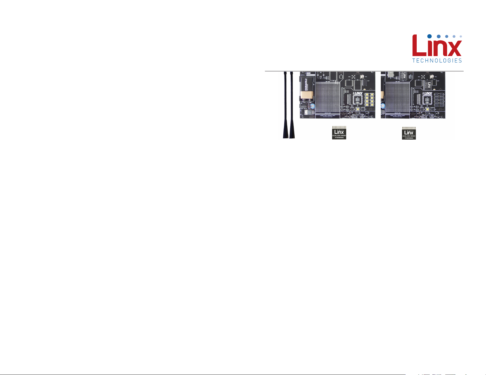
MS Series Master Development System
User's Guide
Figure 1: MS Series Master Development System
Introduction
The MS Series encoders and decoders are ideal for remote control and
command, security, keyless entry, status monitoring and a host of similar
applications. They allow the status of up to eight buttons or contacts to be
securely transferred via a wireless link. The Master Development System
gives a designer all the tools necessary to incorporate the MS Series into a
product. This guide shows how to take full advantage of the development
boards included with the system. The Master Development System serves
several important functions:
• Rapid Evaluation: It allows the performance and features of the MS
Series encoder and decoder to be quickly evaluated.
• Design: It shows how to design with the MS Series and how to
interface with other components. It also demonstrates the overall
system function, making it easy to develop the initial system design.
• Prototype Development: It allows for additional circuitry to be placed
directly on the board so that it can act as the first prototype of the
product. All of the signals are available on a wire-wrap header for easy
connection to external circuitry.
This kit includes 2 development boards, 2 MS Series encoders*, 2 MS
Series decoders*, and two CW Series antennas, 1 LR or ES Series
transmitter, 1 LR or ES Series receiver, full documentation and batteries.
The decoder board is populated with 1 QS Series USB module.
*One part is soldered to the board, one extra is for use on your first prototype board.
– –
1
Revised 3/18/2015
Page 4
Ordering Information
Ordering Information
Part Number Description
MDEV-LICAL-MS MS Series Master Development System with LR Series
MDEV-LICAL-MS-ES MS Series Master Development System with ES Series
Figure 2: Ordering Information
MS Series Deccoder Development Board
5
1
8
9
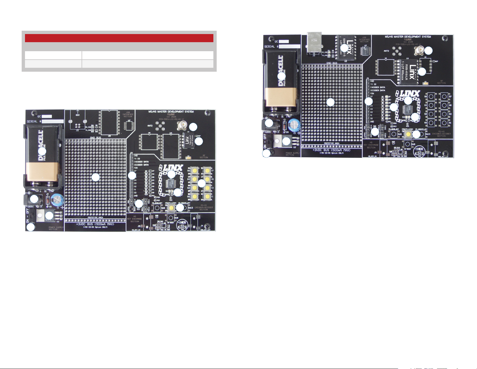
MS Series Encoder Development Board
1
5
2
4
3
Figure 3: MS Series Encoder Development Board
1. 9V Battery
2. Power Jack
3. On-Off Switch
4. Voltage Regulator
5. Prototype Area
6. Break-Out Header
7. Reverse-Polarity SMA Antenna
Connector
6
11
8. LR Series Transmitter Module
9. MS Series Encoder
10. Indicator LEDs
11. Function Switches
12. CREATE Button
13. Data Line Buttons
6
7
8
9
13
10
2
4
3
Figure 4: MS Series Deccoder Development Board
1. 9V Battery
2. Power Jack
3. On-Off Switch
4. Voltage Regulator
12
5. QS Series USB Module
6. Prototype Area
7
13
9. LR Series Receiver Module
10. MS Series Decoder
11. Data Line LEDs
12. Indicator LEDs
13. Function Switches
14. LEARN Button
10
11
12
14
7. Break-Out Header
8. Reverse-Polarity SMA Antenna
Connector
– – – –
2 3
Page 5

Using the Development Boards
Use of the development boards is straightforward. After unpacking the
development system, attach an antenna to each board, install the supplied
9V battery and turn on the power switches. The encoder and decoder
are set at the factory and work straight out of the box. To create a new
address, follow these steps:
1. Press and hold the CREATE button on the encoder board to create a
new Address. The Address is randomized for as long as the button is
held down. Once comfortable that the number is sufficiently random,
release the button.
2. Once the CREATE button is released, the MODE_IND LED begins to
flash to indicate that it is ready to accept Control Permissions. Press
all of the data line buttons that are to be authorized, then press the
CREATE button again or let the encoder time out.
3. Press the LEARN button on the decoder board and the MODE_IND
LED starts flashing. Press any of the data line buttons on the encoder
board and press the LEARN button again or let the decoder time out.
The encoder's Address has been learned by the decoder and they can
now operate together.
Troubleshooting
If the boards fail to work out of the box, then try the following:
• Check the battery to make sure it is not dead.
• Make sure that the baud rate switches are set the same on both
boards.
The Prototyping Area
The prototyping area is the same on both boards and contains a large
area of plated through holes so that external circuitry can be placed
on the board. This circuitry can be interfaced with the MS encoder or
decoder through the header to the right. At the bottom of this area is a row
connected to the 3V power supply and at the top is a row connected to
ground.
All of the data lines are connected to a wire-wrap header to the right,
allowing easy access from the prototyping area. The DATA_IN, DATA_OUT
and TX_ID lines are also available on the header, as well as the PDN lines
from the RF modules. This allows complete control of the entire system
from the prototyping area, giving the designer a great deal of flexibility in
using the boards.
The Power Supply
The power supply is the same on both boards and consists of a standard
9V battery and a power jack connected to a 3.0V voltage regulator. The
regulator can provide approximately 500mA of current to the prototyping
area. If the added circuitry needs more than this, then the designer must
add an external supply. If the circuit consistently draws more than 100mA
of current, it might be better to use the power jack, as the battery may run
down fairly quickly, reducing testing and development time.
The jack accepts a standard 5.5mm plug with the tip ground and the outer
shell 7 to 16VDC positive supply. A reverse voltage protection diode is
included on the board to protect the circuitry in case the voltage on the
plug is reversed, but it is still a good idea to double-check the polarity.
• Make sure that the antenna is connected and has the correct polarity
connector.
• Check to see if the PDN switch is on, placing the encoder and decoder
into Power Down Mode. In most cases, the encoder PDN switch
should be in the up position.
• Make sure that the Control Permissions are set correctly. If the encoder
is not set to use a particular line, then when the button on the encoder
board is pressed, the MODE_IND LED on the decoder board lights up,
but the data line LED does not light up.
If all of these appear to be in order, then call +1 800 736 6677 or email
[email protected] for technical support.
– – – –
4 5
Page 6
The Encoder Board
The encoder board has two sections that are of primary interest: the
encoder area and the transmitter area.
The Encoder Area
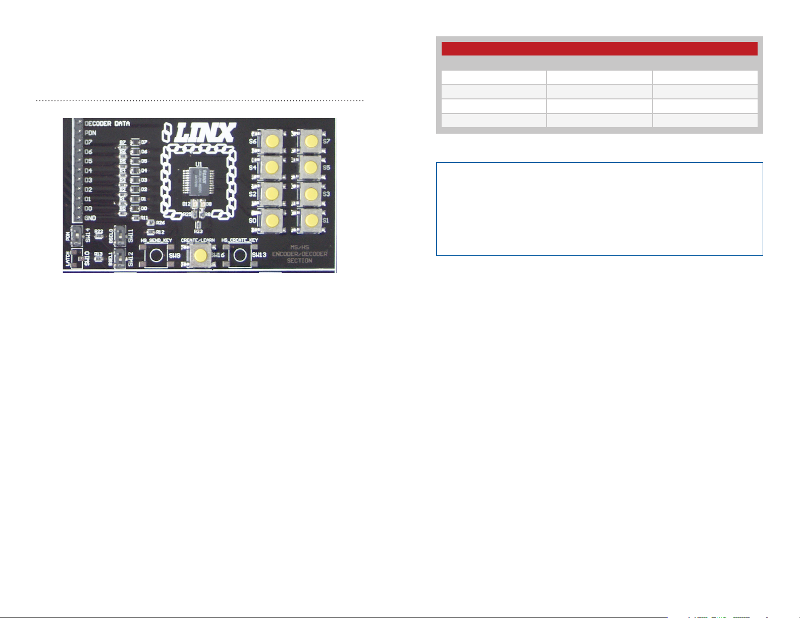
Figure 5 shows the encoder area of the development board.
Figure 5: The Encoder Area
The encoder is placed in the center beneath the Linx logo. To the right are
buttons that pull the encoder data lines high when pressed. Button S0
corresponds to data line D0, S1 to D1 and so forth.
The diodes to the left isolate the data lines from each other while allowing
any line to activate the SEND line.
Beneath the encoder are two LEDs. D12 is connected to the MODE_IND
line and lights up as described in the MS Encoder Data Guide. D8 is
connected to the TX_CNTL line and provides visual feedback by lighting up
when the encoder sends a word.
Baud Rate Selection Table
SEL_BAUD1 SEL_BAUD0 Baud Rate (bps)
0 0 2,400
0 1 9,600
1 0 19,200
1 1 28,800
Figure 6: Baud Rate Selection Table
Note: The decoder board must be set to the same baud rate in order
for the signal to be received correctly. The maximum baud rate for the
LR Series is 10,000bps, so only 2,400 and 9,600bps can be used on
boards populated with these modules. The ES Series transmitter can
use all four baud rates. If the switch is up, then the line is high, if it is
down, then the line is low.
The PDN switch connects the TX_CNTL line of the encoder to the PDN
line of the transmitter so that the TX Control Mode of the encoder can be
tested. This mode is described in the MS Series Encoder Data Guide.
If a BSEL switch is up, then the line is high (1, VCC); if down, then the line
is low (0, GND). If the PDN switch is up, then the encoder’s TX_CNTL line
is connected to the transmitter’s PDN line; if down, it is not connected and
the LR Series transmitter is not activated unless its PDN line is pulled high
externally. The ES Series transmitter has an internal pull-up, so is active
unless pulled low.
Beneath the LEDs is a button that is connected to the CREATE line. This
button is used to create the Address and set the Control Permissions as
described in the MS Series Encoder Data Guide.
There are three function switches to the left of the CREATE button. BSEL0
and BSEL1 are used to set the baud rate of the encoder as described
in Figure 6. The maximum baud rate for the LR Series is 10,000bps, so
only 2,400 and 9,600bps can be used on boards populated with these
modules. The ES Series can use all four baud rates.
– – – –
6 7
Page 7
The Encoder Board RF Area
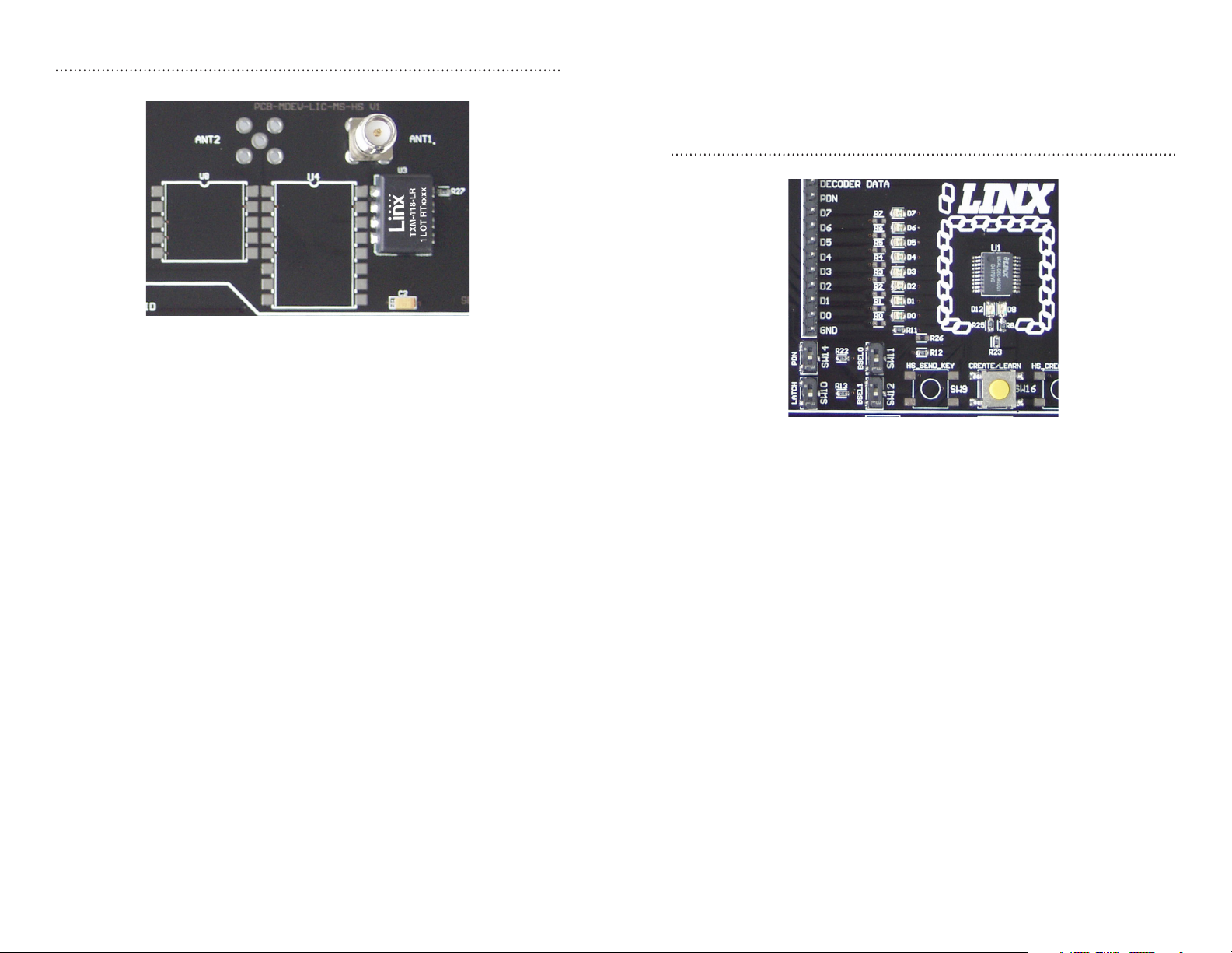
Figure 7 shows the RF area of the development board.
Figure 7: The Encoder Board RF Area
This board can be populated with either the LR Series transmitter (as
shown) or the ES Series transmitter. The LR Series transmitter is placed
on the right side and the ANT1 connector is populated. The ES Series
transmitter is placed on the left and the ANT2 connector is populated.
R27 is connected to the LADJ line of the LR transmitter to reduce the
output power to approximately 0dBm. The LR Series transmitter is capable
of producing more output power than may be legally acceptable, so by
reducing the output power, the range experienced with the evaluation kit
more closely resembles the rage that can be achieved with a final certified
product.
The Decoder Board
The decoder board has three main sections of interest: the decoder area,
the receiver area, and the USB area.
The Decoder Area
Figure 8 shows the decoder area of the development board.
Figure 8: The Decoder Area
The decoder is placed in the center beneath the Linx logo. To the left are
LEDs that are connected to the decoder data lines. These light up when
the decoder receives a signal from the encoder to take the data line high.
LED D0 corresponds to data line D0 and so forth.
Beneath the decoder are two LEDs. D12 is connected to the MODE_IND
line and lights up as described in the MS Series Decoder Data Guide. D8 is
connected to the RX_CNTL line and provides visual feedback by lighting up
when the decoder activates the receiver when in RX Control Mode.
Beneath the LEDs is a button that is connected to the LEARN line. This
button is used to learn the Address from the encoder as described in the
MS Series Decoder Data Guide.
There are four function switches to the left of the CREATE button. BSEL0
and BSEL1 are used to set the baud rate of the decoder as described in
Figure 6.
– – – –
8 9
Page 8
Note: The encoder board must be set to the same baud rate in order
for the signal to be received correctly. The maximum baud rate for the
LR Series is 10,000bps, so only 2,400 and 9,600bps can be used on
boards populated with these modules. The ES Series receiver can use
all four baud rates. If the switch is up, then the line is high, if it is down,
then the line is low.
The PDN switch connects the RX_CNTL line of the encoder to the PDN line
of the receiver so that the RX Control Mode of the decoder can be tested.
This mode is described in the MS Series Decoder Data Guide.
The LATCH switch places the decoder into Latch Mode when on, so that
the data lines will go high when a valid signal is received and stay high
until a second valid signal is received. If the switch is off, the data lines are
momentary.
The Decoder Board RF Area
Figure 9 shows the RF area of the development board.
The Decoder Board USB Area
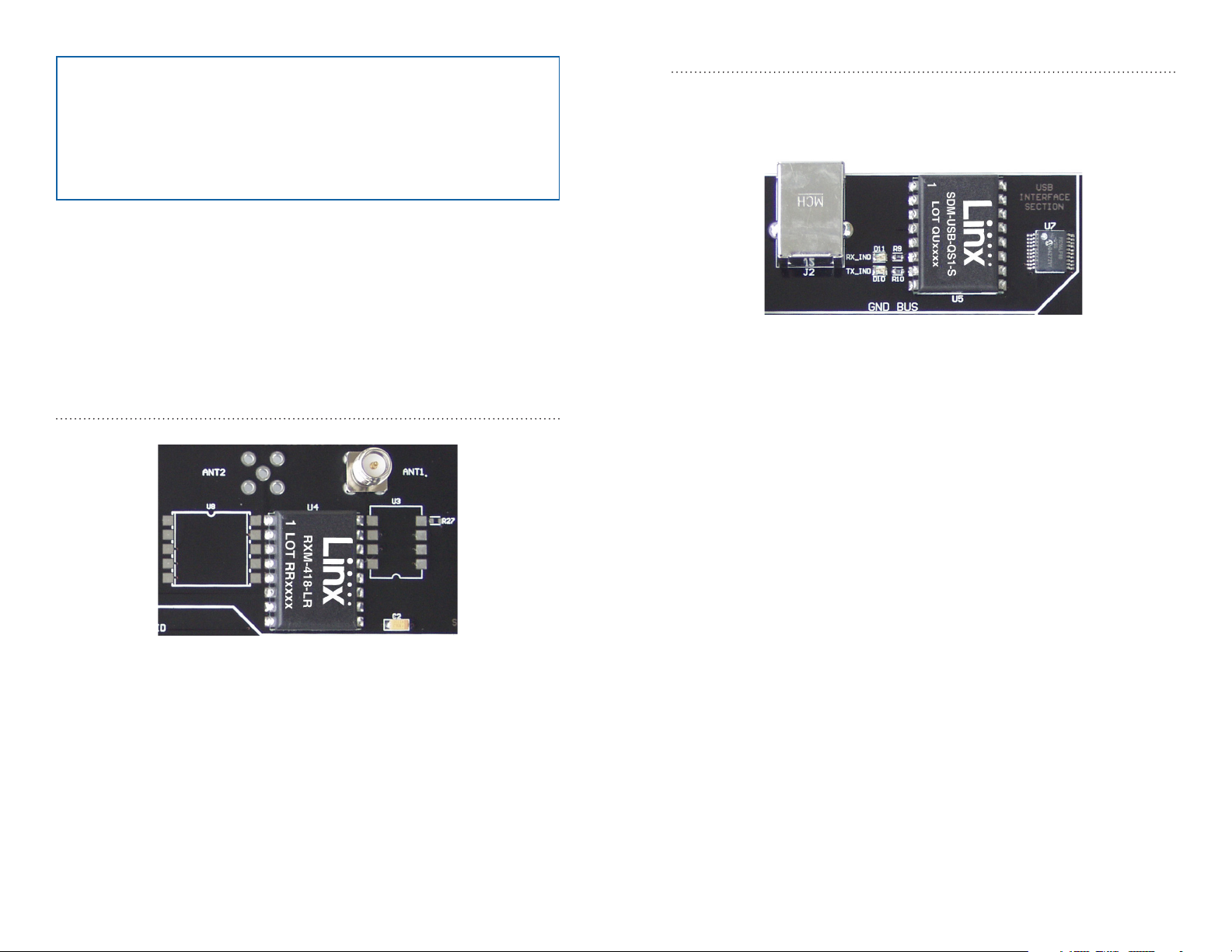
The decoder development board has a Linx SDM-USB-QS USB interface
module for use with the included development software. The module is
powered by the USB bus so does not pull any current from the battery.
Figure 10 shows this section.
Figure 10: The Decoder Board USB Area
The microcontroller on the right monitors the data lines and generates
commands that are sent to the development software on the PC via the
QS Series USB module. The RX_IND LED to the left of the module flashes
to indicate that data is being received from the PC, and the TX_IND line
flashes to indicate that the module is sending data to the PC.
Figure 9: The Decoder Board RF Area
This board can be populated with either the LR Series receiver (as shown)
or the ES Series receiver. Both modules can be placed on the same pads
in the center of the section, but the ANT1 connector is populated for the
LR receiver and the ANT2 connector is populated for the ES receiver.
– – – –
10 11
Page 9
Installing the Software and Drivers
The first time a QS module is plugged into a computer, Windows displays
the Found New Hardware Wizard, which guides the installation of the
drivers. The drivers are included on the CD, so point the wizard to the CD
when prompted. The drivers have not gone through Microsoft’s verification
process, so a message may appear warning of this. Click “Continue
Anyway” to finish the installation process.
Application Note AN-00201 (Installing the SDM-USB-QS-S Drivers)
describes the installation of the drivers in detail. The drivers should be
installed before running the Development Software.
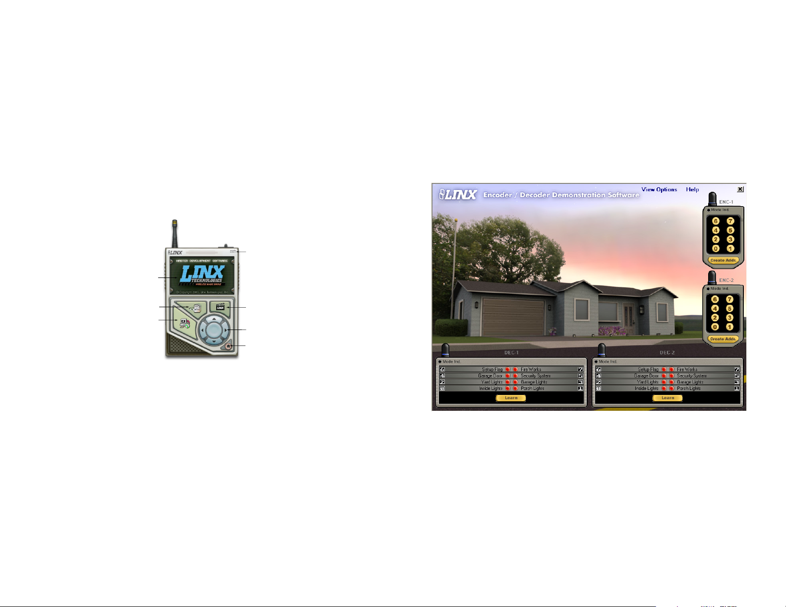
The MS Series Master Development System Software automatically starts
when the CD is inserted and the player in Figure 11 appears.
Exit
Player Screen
MS Series Master Development System Software
The MS Series Master Development System software can be used in one
of two modes. The default mode is as a simulation of the system. This
is a good way of showing how the MS Series can work in a system for
activating lights and doors.
The second mode is for use with the development system. When the
decoder board is plugged into the USB port, the kit can be used to activate
the features in the software. When a data line goes high on the decoder,
the microcontroller sends a command to the computer to control the
functions in the software.
View Documentation
Install Software
Figure 11: Software Installer
Play Movie
Selection Keypad
Go to the
Linx Website
The View Documentation button shows a list of the application notes and
manuals related to the MS Series. Selecting one of these opens the file in
Adobe Acrobat. The Play Movie button plays a short video about Linx in the
Player Screen, which can be controlled with the Selection Keypad. Clicking
the button on the bottom right of the player opens the Linx Technologies
homepage in the computer’s default browser.
The View Documentation list also allows for the installation of Adobe
Acrobat Reader, so that the documents may be viewed, and Flash, which
may be required if the Linx video does not play correctly.
Clicking the Install Software button starts the Installation Wizard, which
guides the installation of the development software. The installer places the
software application, MS Series documentation, and USB drivers at the
installed location on the computer's hard drive.
– – – –
12 13
Figure 12: The MS Series Master Development System Software
Clicking the Help label at the top of the window opens the guide for
using the development software. Please see this document for details on
operation of the software.
Page 10
LATCH
RA2/AN2
1
RA3/AN3
2
RA4/AN4
3
RA5/MCLR
4
GND
5
GND
6
RB0/INT
7
RB1
8
RB2/RX
9
RB3
10
RB4
11
RB5/TX
12
RB6/AN5
13
RB7/AN6
14
VCC
15
VCC
16
RA6
17
RA7
18
RA0/AN0
19
RA1/AN1
20
U7
PIC16LF88
GND
VCC
GND VCC
GND
GND
GND
GND
GND
D7
D4
TX_ID
D6
D3
D0
D1
D2 D5
DATA_PC
PDN
DEC_DATA
GND
GND
VCC
RF1ES RF
1
GND
2
NC
3
GND
4
VCC
5
LR PDN
6
LR RSSI
7
LR DATA
8
NC
9
ES AUDIO REF
10
ES AUDIO
11
ES DATA
12
ES RSSI
13
ES PDN
14
GND
15
LR RF
16
U4
RXM-XXX-LR
RXM-XXX-ES
GND
PDN
DEC_DATA
RF2
ANT1
REVSMAPCB
GND
RF1
ANT2
REVSMAPCB
GND
RF2
DATA_PC
5V
1
DAT -
2
DAT+
3
GND
4
GSHD
5
GSHD
6
J2
USB-B
USBDP
1
USBDM
2
GND
3
VCC
4
SUSP IND
5
RX IND
6
TX IND
7
485 TX
8
DTR
9
CTS
10
RTS
11
DATA OUT
12
DATA IN
13
DSR
14
DCD
15
RI
16
U5
SDM-USB-QS
GND
GND
GNDGND
R9
200
D11
RX_IND
R10
200
D10
TX_ID
B1
9V BATTERY
GND
SW15
POWER SWITCH
GND
+
C1
220uF
GND
VCC
C2
10uF
GND
VCC
D9
DIODE400
Vb
SW Vb
Va
J1
PWRJACK
GND
GND
1
Vout
2
Vin
3
U2
VREG-3V
VREG-5V (ES RX ONLY)
PDN
1
LVL/AM
2
VCC
3
GND
4
DATA
5
/CLK
6
/CLK SEL
7
LV DET
8
GND
9
RF
10
U8
TXM-xxx-ES
GND
VCC
DATA_OUT
PDN RF2
GND
VCC
GND
1
DATA IN
2
GND
3
LADJ/VCC
4
RF OUT
5
GND
6
VCC
7
PDN
8
U3
TXM-xxx-LR
GND
VCC
GND
GND
DATA_OUT
PDN
RF1
R27
620ohm
POWER SUPPLY SECTION
USB SECTION
RF SECTION
B1
9V BATTERY
GND
SW15
POWER SWITCH
GND
+
C1
220uF
GND
VCC
C2
10uF
GND
VCC
D9
DIODE400
Vb
SW Vb
Va
J1
PWRJACK
GND
GND
1
Vout
2
Vin
3
U2
VREG-3V
VREG-5V (ES RX ONLY)
POWER SUPPLY SECTION
USB SECTION
LATCH
RA2/AN2
1
RA3/AN3
2
RA4/AN4
3
RA5/MCLR
4
GND
5
GND
6
RB0/INT
7
RB1
8
RB2/RX
9
RB3
10
RB4
11
RB5/TX
12
RB6/AN5
13
RB7/AN6
14
VCC
15
VCC
16
RA6
17
RA7
18
RA0/AN0
19
RA1/AN1
20
U7
PIC16LF88
GND
VCC
GND VCC
GND
GND
GND
GND
GND
D7
D4
TX_ID
D6
D3
D0
D1
D2 D5
DATA_PC
DATA_PC
5V
1
DAT -
2
DAT+
3
GND
4
GSHD
5
USBDP
1
USBDM
2
GND
3
VCC
4
SUSP IND
5
RX IND
6
TX IND
7
485 TX
8
DTR
9
CTS
10
RTS
11
DATA OUT
12
DATA IN
13
DSR
14
DCD
15
RI
16
U5
SDM-USB-QS
GND
GND
R9
200
D11
RX_IND
R10
200
D10
TX_ID
B1
9V BATTERY
GND
SW15
POWER SWITCH
GND
+
C1
220uF
GND
VCC
C2
10uF
GND
VCC
D9
DIODE400
Vb
SW Vb
Va
J1
PWRJACK
GND
GND
1
Vout
2
Vin
3
U2
VREG-3V
VREG-5V (ES RX ONLY)
POWER SUPPLY SECTION
USB SECTION
RF SECTION
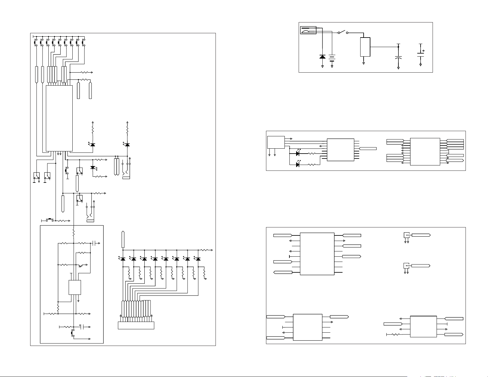
Schematics
VCC
D5
D4S3D3S2D2S1D1S0D0
D7
S4
S6D6S7
S5
D7D4D6
D3D0D1
D5
D5
VCC
D2
D2D3D4
VCC
VCC
D0
D1
VCC
SEND/DEC_DATA_IN
DEC_DATA
CREATE/LEARN
SW16
R23
100K
R26
0K
GND
SEND
J1
Va
Vb
PWRJACK
D9
DIODE400
Figure 14: Power Supply Section
GND
SW Vb
SW15
POWER SWITCH
B1
9V BATTERY
GND
VREG-3V
3
VREG-5V (ES RX ONLY)
Vin
2
U2
Vout
GND
1
GND
VCC
GND
+
C1
220uF
VCC
GND
C2
10uF
U1
D6D7SEL_BAUD0
SW11
SEL_BAUD0
SW12
VCC
VCC
GND
SW9
VCC
HS-ENC
VCC
Figure 13: Figure 11: Encoder / Decoder Section
SEL_BAUD1/HSE_GND/HSD_SEND_KEY
GND
GND
KEY_IN/MSE_GND/MSD_LATCH
TX_CNTL/MSD_RX_CNTL/HSD_CREATE_KEY
DATA_OUT/MSD_TX_ID/HSD_KEY_OUT
MODE_IND CREATE_ADDR/DEC_LEARN
LICAL-XXX-MS
LICAL-XXX-HS
GND
GND
SEL_BAUD1
HS_SEND_KEY
R17
9.1M
R15
SW13
LATCH
R12
100k
R21
R19
9.1M
VCC
SW14
PDN
HS_CREATE_KEY
PDN
VCC
SW10
LATCH
VCC
J5
GND
R28
10K
R18
100K
9.1M
R20
51K
10K
IR1
PS1102
VCC
5
6
7
8
CIN-
VCC
CIN+
COUT
AIN-2AIN+3GND
AOUT
U6
TLV2302
1
4
GND
R16
9.1M
C4
4.7uF
R14
5.1M
SW8
SW-PB
R25
D12
TX_EN
D8
GND
GND
GND
GND
GND
200
MODE_IND
R22
100k
R8
200
100k
R13
GND
HS_KEY_IN
C5
0.01uF
GND
GND
R24
150 ohm
IR2
IR KEY_OUT
GND
GND
TX_ID
DATA_OUT
GND
J4
GND
SEND
D0
GND
J3
– – – –
14 15
HSD_KEY_OUT
D0_INDD1D1_IND
R0
D2_INDD3D3_INDD4D4_INDD5D5_INDD6D6_IND
100KR1100KR2100KR3100KR4100KR5100K
D3D0D1D2D5
1011121314
D2
GND
GND
GND
GND
D7D4D6
DEC_DATA
PDN
DATA_OUT
TX_ID
1
2345678
9
CON14
GND
200
R11
GND
D7_IND
D7
100K
R6
100K
GND
R7
GND
GND
GND
J2
USB-B
GNDGND
Figure 15: USB Section
Figure 16: RF Section
4
GND
GND
3
DAT+
2
DAT -
1
5V
GSHD
GSHD
5
6
PDN RF2
DATA_OUT
RF2
PDN
DEC_DATA
VCC
GND
GND
GND
VCC
D10
1
2
3
4
5
D11
RX_IND
TX_ID
1
2
3
4
5
6
7
8
U8
PDN
LVL/AM
VCC
GND
DATA
TXM-xxx-ES
U4
GND
NC
GND
VCC
LR PDN
LR RSSI
LR DATA
RXM-XXX-LR
RXM-XXX-ES
U5
1
USBDP
2
USBDM
3
GND
GND
4
VCC
5
SUSP IND
R9
6
RX IND
7
200
R10
200
8
TX IND
485 TX
SDM-USB-QS
LR RF
GND
ES PDN
ES RSSI
ES DATA
ES AUDIO
ES AUDIO REF
NC
10
RF
9
GND
8
LV DET
7
/CLK SEL
6
/CLK
16
15
14
13
12
11
10
9
GND
DATA IN
DATA OUT
RF1ES RF
GND
PDN
DEC_DATA
DCD
DSR
RTS
CTS
DTR
16
RI
15
14
13
DATA_PC
12
11
10
9
D3
D2 D5
D1
D0
TX_ID
GND
DATA_OUT
GND
R27
VCC
620ohm
U7
1
RA2/AN2
2
RA3/AN3
3
GND
RA4/AN4
4
GND
RA5/MCLR
5
GND
GND
6
GND VCC
GND
7
RB0/INT
8
RB1
9
RB2/RX
10
GND
RB3
PIC16LF88
ANT1
REVSMAPCB
RF1
RA1/AN1
RA0/AN0
RB7/AN6
RB6/AN5
RB5/TX
20
D4
19
18
D6
RA7
17
D7
RA6
16
VCC
15
VCC
14
LATCH
13
12
DATA_PC
11
RB4
GND
ANT2
REVSMAPCB
RF2
GND
U3
1
GND
2
DATA IN
3
GND
4
LADJ/VCC
TXM-xxx-LR
PDN
VCC
GND
RF OUT
8
PDN
7
VCC
6
GND
5
RF1
VCC
GND
GND
Page 11

Linx Technologies
159 Ort Lane
Merlin, OR, US 97532
Phone: +1 541 471 6256
Fax: +1 541 471 6251
www.linxtechnologies.com
Disclaimer
Linx Technologies is continually striving to improve the quality and function of its products. For this reason, we
reserve the right to make changes to our products without notice. The information contained in this Data Guide
is believed to be accurate as of the time of publication. Specifications are based on representative lot samples.
Values may vary from lot-to-lot and are not guaranteed. “Typical” parameters can and do vary over lots and
application. Linx Technologies makes no guarantee, warranty, or representation regarding the suitability of any
product for use in any specific application. It is the customer’s responsibility to verify the suitability of the part for
the intended application. NO LINX PRODUCT IS INTENDED FOR USE IN ANY APPLICATION WHERE THE SAFETY
OF LIFE OR PROPERTY IS AT RISK.
Linx Technologies DISCLAIMS ALL WARRANTIES OF MERCHANTABILITY AND FITNESS FOR A PARTICULAR
PURPOSE. IN NO EVENT SHALL LINX TECHNOLOGIES BE LIABLE FOR ANY OF CUSTOMER’S INCIDENTAL OR
CONSEQUENTIAL DAMAGES ARISING IN ANY WAY FROM ANY DEFECTIVE OR NON-CONFORMING PRODUCTS
OR FOR ANY OTHER BREACH OF CONTRACT BY LINX TECHNOLOGIES. The limitations on Linx Technologies’
liability are applicable to any and all claims or theories of recovery asserted by Customer, including, without
limitation, breach of contract, breach of warranty, strict liability, or negligence. Customer assumes all liability
(including, without limitation, liability for injury to person or property, economic loss, or business interruption) for
all claims, including claims from third parties, arising from the use of the Products. The Customer will indemnify,
defend, protect, and hold harmless Linx Technologies and its officers, employees, subsidiaries, affiliates,
distributors, and representatives from and against all claims, damages, actions, suits, proceedings, demands,
assessments, adjustments, costs, and expenses incurred by Linx Technologies as a result of or arising from any
Products sold by Linx Technologies to Customer. Under no conditions will Linx Technologies be responsible for
losses arising from the use or failure of the device in any application, other than the repair, replacement, or refund
limited to the original product purchase price. Devices described in this publication may contain proprietary,
patented, or copyrighted techniques, components, or materials. Under no circumstances shall any user be
conveyed any license or right to the use or ownership of such items.
©2015 Linx Technologies. All rights reserved.
The stylized Linx logo, Wireless Made Simple, WiSE, CipherLinx and the stylized CL logo are trademarks of Linx Technologies.
 Loading...