

Page 1

GPS / GNSS Receiver Master
Development System
User's Guide
Page 2

Warning: Some customers may want Linx radio frequency (“RF”)
!
products to control machinery or devices remotely, including machinery
or devices that can cause death, bodily injuries, and/or property
damage if improperly or inadvertently triggered, particularly in industrial
settings or other applications implicating life-safety concerns (“Life and
Property Safety Situations”).
Table of Contents
1 Introduction
2 Ordering Information
3 Receiver Development Board
NO OEM LINX REMOTE CONTROL OR FUNCTION MODULE
SHOULD EVER BE USED IN LIFE AND PROPERTY SAFETY
SITUATIONS. No OEM Linx Remote Control or Function Module
should be modified for Life and Property Safety Situations. Such
modification cannot provide sufficient safety and will void the product’s
regulatory certification and warranty.
Customers may use our (non-Function) Modules, Antenna and
Connectors as part of other systems in Life Safety Situations, but
only with necessary and industry appropriate redundancies and
in compliance with applicable safety standards, including without
limitation, ANSI and NFPA standards. It is solely the responsibility
of any Linx customer who uses one or more of these products to
incorporate appropriate redundancies and safety standards for the Life
and Property Safety Situation application.
Do not use this or any Linx product to trigger an action directly
from the data line or RSSI lines without a protocol or encoder/
decoder to validate the data. Without validation, any signal from
another unrelated transmitter in the environment received by the
module could inadvertently trigger the action.
All RF products are susceptible to RF interference that can prevent
communication. RF products without frequency agility or hopping
implemented are more subject to interference. This module does not
have a frequency hopping protocol built in.
3 Board Objects
4 Initial Setup
4 Troubleshooting
5 The Prototyping Area
6 The Receiver Section
7 The USB Section
8 The Display Section
9 Master Development Software
10 Schematics
Do not use any Linx product over the limits in this data guide.
Excessive voltage or extended operation at the maximum voltage could
cause product failure. Exceeding the reflow temperature profile could
cause product failure which is not immediately evident.
Do not make any physical or electrical modifications to any Linx
product. This will void the warranty and regulatory and UL certifications
and may cause product failure which is not immediately evident.
Page 3
GPS/GNSS Master Development System
User's Guide
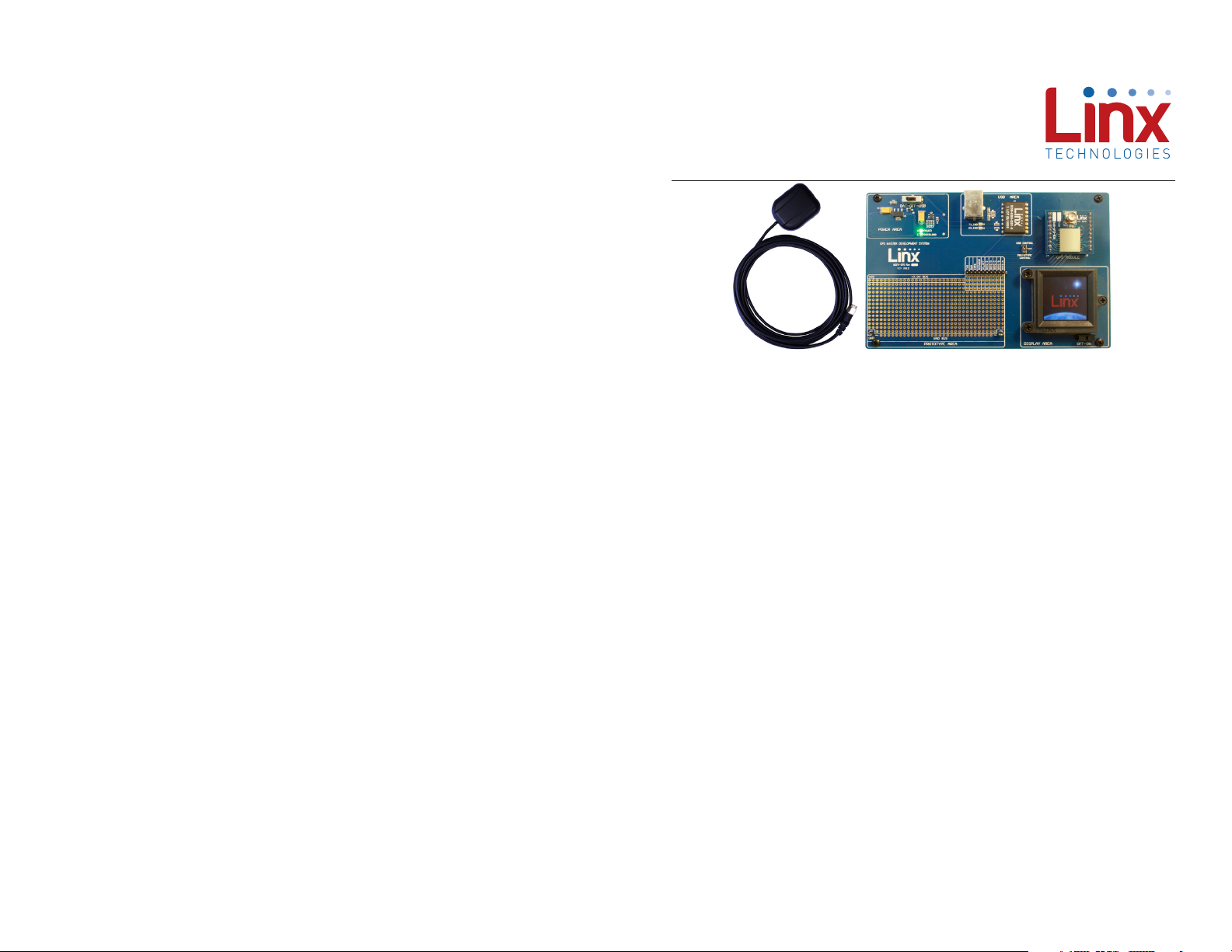
Figure 1: GPS / GNSS Master Development System
Introduction
The Linx GPS and GNSS modules offer a simple, efficient and
cost-effective method of adding GPS or GNSS capabilities to any product.
The Master Development System is intended to give a designer all the tools
necessary to correctly incorporate the modules into an end product. The
development boards themselves serve several important functions:
• Rapid Module Evaluation: The boards allow the performance of the
modules to be evaluated quickly in a user’s environment.
• Application Development: An onboard prototyping area allows for the
development of custom circuits directly on the development board. All
signal lines are available on a header for easy access.
• Design Benchmark: The boards provide a known benchmark against
which the performance of a custom design may be judged.
The Master Development System includes one assembled development
board, one receiver module on an evaluation board, one spare receiver
module for use on your first prototype, one SH Series active GPS antenna,
4 AAA batteries and full documentation.
1
– –
Revised 3/18/2015
Page 4
Ordering Information
Receiver Development Board
Ordering Information
Part Number Description
MDEV-GPS-R4 R4 Series Master Development System
MDEV-GPS-F4 F4 Series Master Development System
MDEV-GPS-RM RM Series Master Development System
MDEV-GPS-FM FM Series Master Development System
MDEV-GNSS-GM GM Series Master Development System
MDEV-GNSS-TM TM Series Master Development System
EVM-GPS-R4 R4 Series Evaluation Module
EVM-GPS-F4 F4 Series Evaluation Module
EVM-GPS-RM RM Series Evaluation Module
EVM-GPS-FM FM Series Evaluation Module
EVM-GNSS-GM GM Series Evaluation Module
EVM-GNSS-TM TM Series Evaluation Module
RXM-GPS-R4-x R4 Series GPS Receiver Module
RXM-GPS-F4-x F4 Series GPS Receiver Module
RXM-GPS-RM-x RM Series GPS Receiver Module
RXM-GPS-FM-x FM Series GPS Receiver Module
RXM-GNSS-GM-x GM Series GNSS Receiver Module
RXM-GNSS-TM-x TM Series GNSS Receiver Module
Figure 2: Ordering Information
2
3
1
6
5
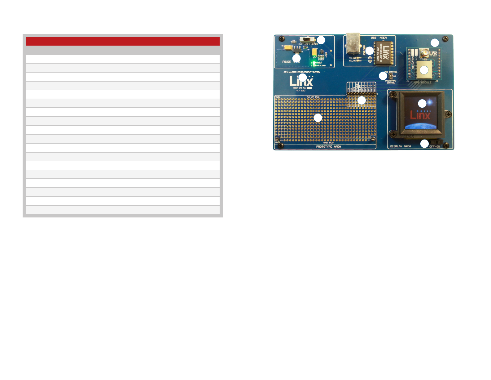
Figure 3: Receiver Development Board
Board Objects
1. Four AAA Batteries (on back)
2. Power Switch
3. Voltage Regulator
4. USB Interface Module
5. Prototype Area
6. Break-Out Header
7. Receiver Evaluation Board
8. CR2032 Backup Battery (on back)
9. Module Data Routing Switch
10. OLED Display
11. OLED Display Power Switch
8
4
7
9
10
11
– – – –
2
3
Page 5
Initial Setup
Unpack the development system and install the AAA and coin-cell
batteries. Connect the external GPS antenna. The power switch selects
between the battery pack or USB power if the board is plugged into a
USB bus. To use the display, turn the OLED display power switch on. The
development board is now ready for use. After turning on the power, the
module determines its current position. Please note, the time required for
an initial fix or after long periods of storage is considerably greater than in
subsequent operation. Please refer to the module’s data guide for complete
information regarding Time-To-First-Fix (TTFF). To protect the display and
extend its life, turn off the display before turning off the board.
Troubleshooting
If the boards fail to work out of the box, then try the following:
• Check the batteries to make sure they are not dead
• Check to make sure that the power switch is in the correct position
• Check that the antenna is installed correctly
• Check that the data routing switch is set appropriately
If all of these appear to be in order, please call +1 800 736 6677 or e-mail
[email protected] for technical support.
The Prototyping Area
In addition to its evaluation functions, the board may also be used for
actual product development. It features a prototyping area to facilitate the
addition of application-specific circuitry. The prototyping area contains a
large area of plated through-holes so that external circuitry can be placed
on the board. The holes are set at 0.100” on center with a 0.040” diameter,
making it easy to add most industry-standard SIP and DIP packages.
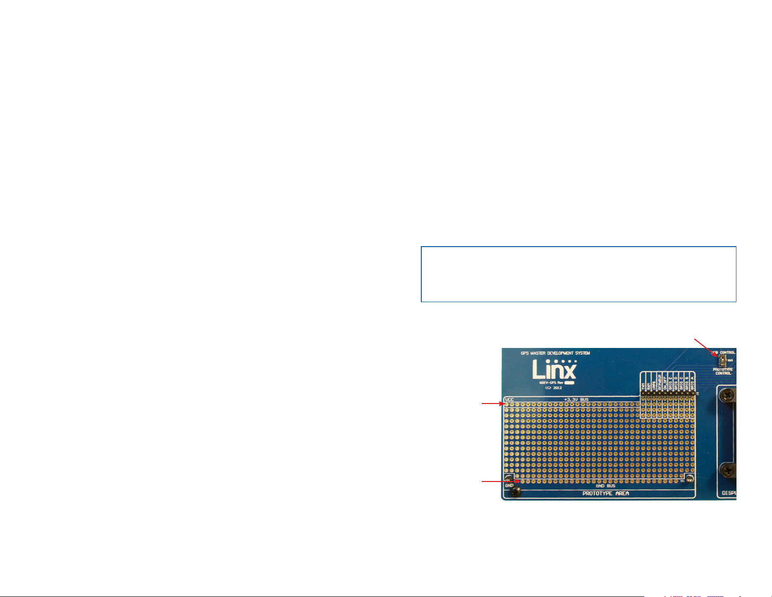
External circuitry can be easily interfaced with the receiver through the
breakout header (J3) on the upper right of the prototyping area. A switch
controls the routing of data into the receiver module. By default the switch
is set for operation with the on-board USB module. When communicating
with the module from the prototyping area this switch should be set
to Prototype Control. At the bottom of the prototyping area is a row
connected to ground and at the top is a row connected to the 3.3V power
supply.
Note: The on-board 3.3-volt regulator has approximately 300mA of
headroom available for additional circuitry. If added circuitry requires a
higher current, the user must add an additional regulator to the prototype
area or power the board from an external supply.
Data Routing
Switch
+3 Volt Bus
Ground Bus
Figure 4: The Development Board Prototyping Area
– – – –
4
5
Page 6
The Receiver Section
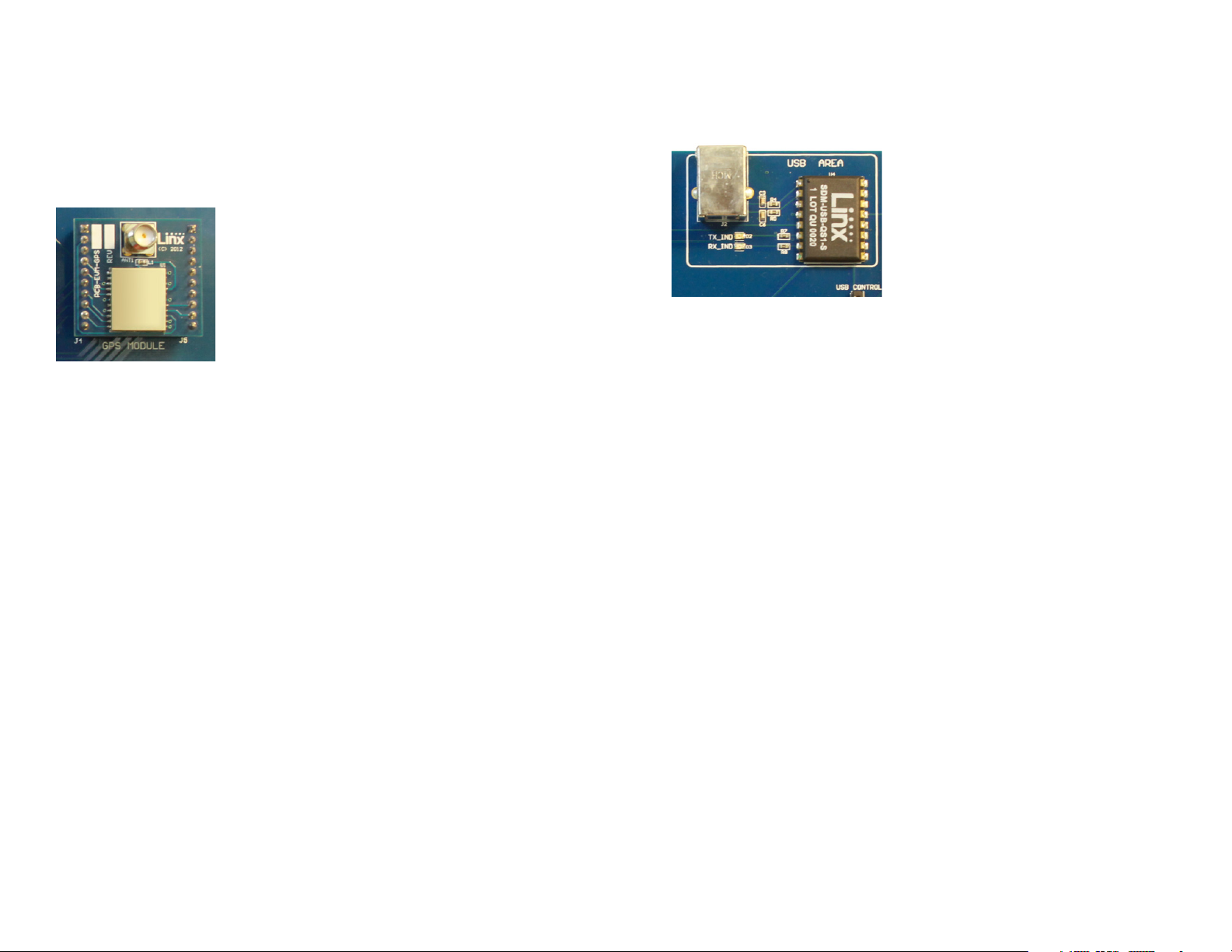
The receiver module is mounted on an evaluation board which plugs into
headers on the main development board. The evaluation board has an
SMA antenna connector to allow the attachment of many different styles of
GPS antennas, including the included SH Series active GPS antenna. Each
receiver module has its own evaluation board, but all of them are designed
to fit into the same socket on the main board.
Figure 5: The Development Board Receiver Section
On the bottom of the main board is a CR2032 coin cell battery that
provides power to the Real Time Clock (RTC) and SRAM when the receiver
is powered down. This allows the receiver to start up and obtain a position
fix faster. This cell provides about two years of operation.
The USB Section
The development board features a Linx QS Series USB module for
interface to a PC. This allows the board to be used with the supplied
development software or with custom software developed by the user.
Figure 6: The Development Board USB Section
Drivers for the USB module are included on the software CD in the kit
or may be downloaded from www.linxtechnologies.com. Additional
information on using the QS Series USB module can also be found on the
website.
The USB connection also allows the board to be powered by the USB
bus instead of batteries. This can be convenient during development to
eliminate the need for frequent battery replacement.
– – – –
6
7
Page 7
The Display Section
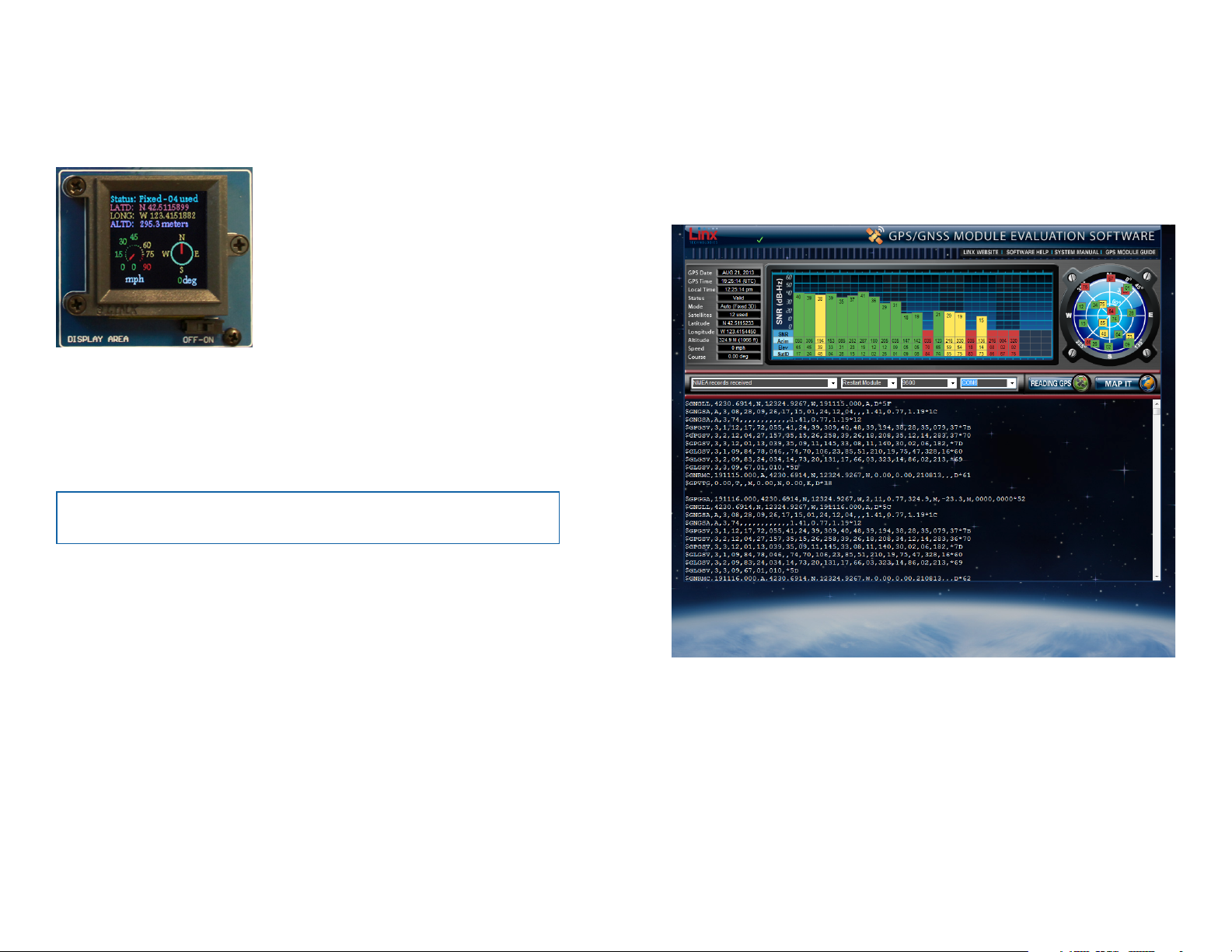
The Master Development System features an OLED screen that displays
the navigation information from the receiver module. This allows the
development board to act as a stand-alone evaluation system without the
need for any additional software.
Figure 7: The Development Board Display Section
The display is driven by an on-board microcontroller located under
the display. Data from the receiver module is connected directly to this
microcontroller. The microcontroller receives data at the receiver’s default
9,600bps.
Note: If the receiver’s baud rate is changed, it will not be able to
communicate with the microcontroller.
Master Development Software
The development system is supplied with Windows-based software that
communicates with the development board through the USB module. This
software displays the information from the receiver module in the different
NMEA formats and the satellite information, signal strength, and positions
are displayed graphically. If the PC is connected to the internet, the
software plots the current location on Google Maps. Full details are in the
software’s User’s Guide.
The display and microcontroller pull about 100mA when fully powered, so
a power switch is supplied to deactivate the display area when not in use,
saving battery life. To protect the display and extend its life, be sure to turn
the display section off before turning off the main power to the board.
– – – –
8
Figure 8: Master Development Software
9
Page 8
+
D4D3D2D1D0
E/RD#
R/W#
VCC
C15
10uF
GND
EN
PMD5/RE5
SOSC0/T1CK/CN0/RC14
OC2/RD1
49
OC3/RD2
50
PMBE/OC4/RD3
51
52
PMRD/CN14/RD5
53
CN15/RD6
54
CN16/RD7
55
VCAP/VDDCORE
56
ENVREG
57
RF058RF1
59
PMD0/RE0
60
PMD1/RE1
61
PMD2/RE2
62
PMD3/RE3
63
PMD4/RE4
64
1
48
D5
B2
BATHLD-001
GND
VBACKUP
1
2
3
4
5
6
7
8
9
10
J5
GND
GND
VCC
VBACKUP
1
2
3
4
5
6
7
8
9
10
J4
GND
GND
TXM
RXM
ON_OFF
1PPS
RESET
RFPWRUP
+
D4D3D2D1D0
E/RD#
R/W#
VCC
C15
10uF
GND
EN
VDD
VSS
PMD5/RE5
PMD6/RE6
PMD7/RE7
PMA5/SCK2/CN8/RG6
PMA4/SDI2/CN9/RG7
PMA3/SDO2/CN10/RG8
MCLR
PMA2/SS2/CN11/RG9
VSS
VDD
C1IN+/AN5/CN7/RB5
C1IN-/AN4/CN6/RB4
SCL1/RG2
OSC1/CLKI/RC12
OSC2/CLKO/RC15
IC1/RTCC/INT1/RD8
IC2/U1CTS/INT2/RD9
IC3/PMCS2/INT3/RD10
IC4/PMCS1/INT4/RD11
OC1/RD0
SOSCI/CN1/RC13
SOSC0/T1CK/CN0/RC14
OC2/RD1
49
OC3/RD2
50
PMBE/OC4/RD3
51
PMWR/OC5/IC5/CN13/RD4
52
PMRD/CN14/RD5
53
CN15/RD6
54
CN16/RD7
55
VCAP/VDDCORE
56
ENVREG
57
RF058RF1
59
PMD0/RE0
60
PMD1/RE1
61
PMD2/RE2
62
PMD3/RE3
63
PMD4/RE4
64
U5
SW2
POWER SWITCH
VCC
1
2
3
4
5
6
7
8
9
10
11
12
13
36
37
38
39
40
41
42
43
44
45
46
47
48
D7
D6
D5
RES#
GND
GND
VCC
VCC
VPP
SW2
GND
VCC
GND
VCC
D8
R14
100k
GPIOD
GPIOE
GPIOC
GPIOB
GPIOA
B2
BATHLD-001
GND
VBACKUP
1
2
3
4
5
6
7
8
9
10
J5
GND
GND
VCC
VBACKUP
1
2
3
4
5
6
7
8
9
10
J4
GND
GND
TXM
RXM
ON_OFF
1PPS
RESET
RFPWRUP
+
1
2
3
4
5
J6
GND
VCC13
C12
4.7uF
VCC
GND
VCC
VCOMH
VDDIO
VSL
+
D4D3D2D1D0
E/RD#
R/W#
VCC
C15
10uF
GND
EN
D/C#
AVSS
VSS
VDD
VDD
VSS
PMD5/RE5
PMD6/RE6
PMD7/RE7
PMA5/SCK2/CN8/RG6
PMA4/SDI2/CN9/RG7
PMA3/SDO2/CN10/RG8
MCLR
PMA2/SS2/CN11/RG9
VSS
VDD
C1IN+/AN5/CN7/RB5
C1IN-/AN4/CN6/RB4
C2IN+/AN3/CN5/RB3
C2IN-/AN2/SS1/CN4/RB2
PGC1/EMUC1/VREF-/AN1/CN3/RB1
PGD1/EMUD1/PMA6/VREF+/AN0/CN2/RB0
PGC2/EMUC2/AN6/OCFA/RB6
PGD2/EMUD2/AN7/RB7
AVDD
U2CTS/C1OUT/AN8/RB8
PMA7/C2OUT/AN9/RB9
TMS/PMA13/CVREF/AN10/RB10
TDO/PMA12/AN11/RB11
TCK/PMA11/AN12/RB12
TDI/PMA10/AN13/RB13
PMA1/U2RTS/BCLK2/AN14/RB14
PMA0/AN15/OCFB/CN12/RB15
PMA9/U2RX/SDA2/CN17/RF4
PMA8/U2TX/SCL2/CN18/RF5
U1TX/SDO1/RF3
U1RX/SDI1/RF2
U1RTS/BCLK1/SCK1/INT0/RF6
SDA1/RG3
SCL1/RG2
OSC1/CLKI/RC12
OSC2/CLKO/RC15
IC1/RTCC/INT1/RD8
IC2/U1CTS/INT2/RD9
IC3/PMCS2/INT3/RD10
IC4/PMCS1/INT4/RD11
OC1/RD0
SOSCI/CN1/RC13
SOSC0/T1CK/CN0/RC14
OC2/RD1
49
OC3/RD2
50
PMBE/OC4/RD3
51
PMWR/OC5/IC5/CN13/RD4
52
PMRD/CN14/RD5
53
CN15/RD6
54
CN16/RD7
55
VCAP/VDDCORE
56
ENVREG
57
RF058RF1
59
PMD0/RE0
60
PMD1/RE1
61
PMD2/RE2
62
PMD3/RE3
63
PMD4/RE4
64
U5
SW2
POWER SWITCH
VCC
1
2
3
4
5
6
7
8
9
10
11
12
13
14
15
16
171819202122232425262728293031
32
33
34
35
36
37
38
39
40
41
42
43
44
45
46
47
48
D7
D6
D5
CS#
RES#
GND
GND GND
GND
VCC
VCCVCC
VCC
VPP
PGC
PGD
TXM
SW2
GND
VCC
GND
VCC
D8
R14
100k
GPIOD
GPIOE
GPIOC
GPIOB
GPIOA
1
2
3
4
5
6
7
8
9
10
J3
TXM
RXMHDR
ON_OFF
1PPS
RFPWRUP
GPIOC
GPIOE
GPIOB
GPIOA
GPIOD
SW3
RXM
RXMHDR
RXMUSB
GND
+
VCC
C14
10uF
Schematics
B2
BATHLD-001
GND
VBACKUP
1
2
3
4
5
6
7
8
9
10
J5
GND
GND
VCC
VBACKUP
1
2
3
4
5
6
7
8
9
10
J4
GND
GND
TXM
RXM
ON_OFF
1PPS
RESET
RFPWRUP
+
1
2
3
4
5
6
7
8
9
10
11
12
13
14
15
16
17
18
19
20
21
22
23
24
25
26
27
28
29
30
J6
GND
VCC13
C12
4.7uF
D7
D6
D5
D4
D3
D2
D1
D0
E/RD#
R/W#
BS0
BS1
CS#
D/C#
RES#
GPIO1
GPIO0
R12
560k
C11
1uF
VCC
VCC
GND
GND
GND
GND
GND
C13
0.1uF
GND
D6
D7
R13
51
GND
GND
VCC
VCC
VCOMH
VDDIO
VSL
IREF
VDD
VCI
VSS
+
D4D3D2D1D0
E/RD#
R/W#
VCC
C15
10uF
GND
EN
D/C#
AVSS
VSS
VDD
VDD
VSS
PMD5/RE5
PMD6/RE6
PMD7/RE7
PMA5/SCK2/CN8/RG6
PMA4/SDI2/CN9/RG7
PMA3/SDO2/CN10/RG8
MCLR
PMA2/SS2/CN11/RG9
VSS
VDD
C1IN+/AN5/CN7/RB5
C1IN-/AN4/CN6/RB4
C2IN+/AN3/CN5/RB3
C2IN-/AN2/SS1/CN4/RB2
PGC1/EMUC1/VREF-/AN1/CN3/RB1
PGD1/EMUD1/PMA6/VREF+/AN0/CN2/RB0
PGC2/EMUC2/AN6/OCFA/RB6
PGD2/EMUD2/AN7/RB7
AVDD
U2CTS/C1OUT/AN8/RB8
PMA7/C2OUT/AN9/RB9
TMS/PMA13/CVREF/AN10/RB10
TDO/PMA12/AN11/RB11
TCK/PMA11/AN12/RB12
TDI/PMA10/AN13/RB13
PMA1/U2RTS/BCLK2/AN14/RB14
PMA0/AN15/OCFB/CN12/RB15
PMA9/U2RX/SDA2/CN17/RF4
PMA8/U2TX/SCL2/CN18/RF5
U1TX/SDO1/RF3
U1RX/SDI1/RF2
U1RTS/BCLK1/SCK1/INT0/RF6
SDA1/RG3
SCL1/RG2
OSC1/CLKI/RC12
OSC2/CLKO/RC15
IC1/RTCC/INT1/RD8
IC2/U1CTS/INT2/RD9
IC3/PMCS2/INT3/RD10
IC4/PMCS1/INT4/RD11
OC1/RD0
SOSCI/CN1/RC13
SOSC0/T1CK/CN0/RC14
OC2/RD1
49
OC3/RD2
50
PMBE/OC4/RD3
51
PMWR/OC5/IC5/CN13/RD4
52
PMRD/CN14/RD5
53
CN15/RD6
54
CN16/RD7
55
VCAP/VDDCORE
56
ENVREG
57
RF058RF1
59
PMD0/RE0
60
PMD1/RE1
61
PMD2/RE2
62
PMD3/RE3
63
PMD4/RE4
64
U5
SW2
POWER SWITCH
VCC
1
2
3
4
5
6
7
8
9
10
11
12
13
14
15
16
171819202122232425262728293031
32
33
34
35
36
37
38
39
40
41
42
43
44
45
46
47
48
D7
D6
D5
CS#
RES#
GND
GND GND
GND
VCC
VCCVCC
VCC
VPP
PGC
PGD
TXM
SW2
GND
VCC
GND
VCC
D8
R14
100k
GPIOD
GPIOE
GPIOC
GPIOB
GPIOA
1
2
3
4
5
6
7
8
9
10
J3
TXM
RXMHDR
ON_OFF
1PPS
RFPWRUP
GPIOC
GPIOE
GPIOB
GPIOA
GPIOD
SW3
RXM
RXMHDR
RXMUSB
5V
1
DAT-
2
DAT+
3
GND
4
GSHD
5
GSHD
6
J2
USB-B
GND
R1
0
RIUSBDP
1
USBDM
2
GND
3
VCC
4
SUSP IND
5
RX IND
6
TX IND
7
485 TX
8
DTR
9
CTS
10
RTS
11
DATA OUT
12
DATA IN
13
DSR
14
DCD
15
16
U4
SDM-USB-QS
RXM USB
TXM
+
GND
GND
C4
4.7uF
C2
0.01uF
L1
GND GND GND
R4 10
C6
10pF
/FAULT
R3
100k
SUSP IND
TX IND
RX IND
C7
0.1uF
C3
10pF
R5 10
4
5
6
+
VCCU
R7 200
D2 TX_IND
D3 RX_IND
R8 200IN
1
GND
2
EN3/FAULT
ILIM
OUT
U2
TPS2553
GND
/FAULT
SUSP IND
GND
GND
TX IND
RX IND
/FAULT
D4 Over Current
R9 200
C1
0.1uF
R6
53.6k
C17
100uF
GND
+
VCC
GND
C14
10uF
GND
SW1
GPIOD
GPIOE
TXM
RXM
1PPS
RESET
RFPWRUP
ON_OFF
GND
J2
USB-B
GSHD
5
6
R1
0
GND
D9
U1
1
C16
10uF
GND
GND
DAT+
DAT-
GSHD
Vin
GND
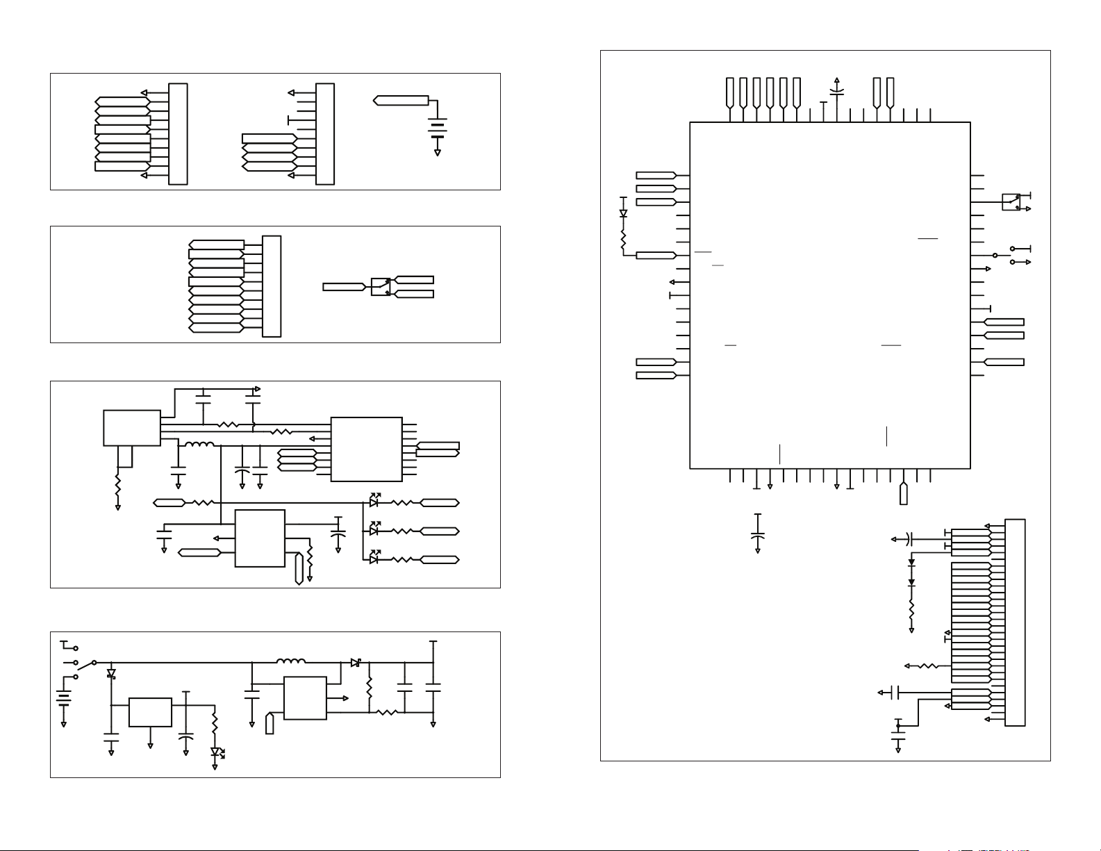
Figure 9: Receiver Section Schematic
Figure 10: Header Section Schematic
Figure 11: USB Section Schematic
VCCU
B1
GND
Figure 12: Power Supply Schematic
J4
1
2
3
4
5
6
7
8
9
10
RXMHDR
RFPWRUP
ON_OFF
4
3
2
1
5V
L1
C2
0.01uF
GND GND GND
/FAULT
GND
C1
0.1uF
R3
100k
GND
SUSP IND
VCC
3
Vout
GND
+
2
C5
100uF
GND
GND
GND
VCC
VBACKUP
GPIOC
GPIOB
GPIOA
GND
J5
1
2
3
4
5
6
7
8
9
10
J3
TXM
1PPS
GPIOE
GPIOD
GPIOC
GPIOB
GPIOA
C3
10pF
R4 10
4.7uF
R2
200
1
2
GRN
1
2
3
4
5
6
7
8
9
10
GND
C6
10pF
R5 10
GND
SUSP IND
TX IND
C7
+
C4
D1
U2
TPS2553
RX IND
GND
EN3/FAULT
GND GND
0.1uF
6
OUT
5
ILIM
4
/FAULT
L2 10uH
U3
5
VIN
C8
10uF
EN4FB
EN
– – – –
10
U4
1
2
USBDM
3
GND
4
VCC
5
SUSP IND
6
RX IND
7
TX IND
8
485 TX
SDM-USB-QS
VCCU
+
GND
R6
53.6k
1
SW
2
GND
3
RXM
C17
100uF
D5
GND
VBACKUP
SW3
RIUSBDP
DCD
DSR
DATA IN
DATA OUT
RTS
CTS
DTR
R7 200
D2 TX_IND
R8 200IN
D3 RX_IND
R9 200
D4 Over Current
R10
47.5k
R11
4.99k
RXMHDR
RXMUSB
16
15
14
13
12
11
10
9
C9
10uF
GND
TXM
RXM USB
TX IND
RX IND
/FAULT
VCC13
C10
0.1uF
B2
BATHLD-001
GND
+
VCC
EN
56
57
59
RF058RF1
ENVREG
VCAP/VDDCORE
U5
PMA7/C2OUT/AN9/RB9
TMS/PMA13/CVREF/AN10/RB10
TDO/PMA12/AN11/RB11
VSS
11
C15
10uF
E/RD#
R/W#
55
CN15/RD654CN16/RD7
TCK/PMA11/AN12/RB12
VDD
VCCVCC
GND
50
51
52
53
OC3/RD2
PMBE/OC4/RD3
PMRD/CN14/RD5
SOSC0/T1CK/CN0/RC14
SOSCI/CN1/RC13
PMWR/OC5/IC5/CN13/RD4
IC4/PMCS1/INT4/RD11
IC3/PMCS2/INT3/RD10
IC2/U1CTS/INT2/RD9
IC1/RTCC/INT1/RD8
OSC2/CLKO/RC15
OSC1/CLKI/RC12
U1RTS/BCLK1/SCK1/INT0/RF6
TDI/PMA10/AN13/RB13
PMA1/U2RTS/BCLK2/AN14/RB14
PMA0/AN15/OCFB/CN12/RB15
PMA9/U2RX/SDA2/CN17/RF4
D/C#
C12
4.7uF
GND
+
D6
D7
R13
51
GND
R12
GND
560k
C11
1uF
VCC
C13
0.1uF
GND
49
OC2/RD1
OC1/RD0
SCL1/RG2
SDA1/RG3
U1RX/SDI1/RF2
U1TX/SDO1/RF3
PMA8/U2TX/SCL2/CN18/RF5
32
VCC13
VCC
GND
VCC
GND
48
47
46
45
44
43
42
41
VSS
40
39
38
VDD
37
36
35
34
TXM
33
GND
VCC
VCOMH
VDDIO
VSL
D7
D6
D5
D4
D3
D2
D1
D0
E/RD#
R/W#
BS0
BS1
CS#
D/C#
RES#
IREF
GPIO1
GPIO0
VDD
VCI
VSS
GND
SW2
SW2
POWER SWITCH
GND
VCC
RES#
CS#
J6
1
2
3
4
5
6
7
8
9
10
11
12
13
14
15
16
17
18
19
20
21
22
23
24
25
26
27
28
29
30
VCC
GND
VCC
GND
1
D5
VCC
D8
R14
100k
Figure 13: Display Section Schematic
2
D6
3
D7
4
5
6
7
VPP
8
9
GND
10
VCC
11
12
13
14
15
PGC
16
PGD
D4D3D2D1D0
63
64
PMD4/RE4
PMD5/RE5
PMD6/RE6
PMD7/RE7
PMA5/SCK2/CN8/RG6
PMA4/SDI2/CN9/RG7
PMA3/SDO2/CN10/RG8
MCLR
PMA2/SS2/CN11/RG9
VSS
VDD
C1IN+/AN5/CN7/RB5
C1IN-/AN4/CN6/RB4
C2IN+/AN3/CN5/RB3
C2IN-/AN2/SS1/CN4/RB2
PGC1/EMUC1/VREF-/AN1/CN3/RB1
PGD1/EMUD1/PMA6/VREF+/AN0/CN2/RB0
PGC2/EMUC2/AN6/OCFA/RB6
171819202122232425262728293031
60
61
62
PMD0/RE0
PMD1/RE1
PMD2/RE2
PMD3/RE3
PGD2/EMUD2/AN7/RB7
AVDD
AVSS
U2CTS/C1OUT/AN8/RB8
GND GND
VCC
+
C14
10uF
GND
Page 9

Linx Technologies
159 Ort Lane
Merlin, OR, US 97532
Phone: +1 541 471 6256
Fax: +1 541 471 6251
www.linxtechnologies.com
Disclaimer
Linx Technologies is continually striving to improve the quality and function of its products. For this reason, we
reserve the right to make changes to our products without notice. The information contained in this Data Guide
is believed to be accurate as of the time of publication. Specifications are based on representative lot samples.
Values may vary from lot-to-lot and are not guaranteed. “Typical” parameters can and do vary over lots and
application. Linx Technologies makes no guarantee, warranty, or representation regarding the suitability of any
product for use in any specific application. It is the customer’s responsibility to verify the suitability of the part for
the intended application. NO LINX PRODUCT IS INTENDED FOR USE IN ANY APPLICATION WHERE THE SAFETY
OF LIFE OR PROPERTY IS AT RISK.
Linx Technologies DISCLAIMS ALL WARRANTIES OF MERCHANTABILITY AND FITNESS FOR A PARTICULAR
PURPOSE. IN NO EVENT SHALL LINX TECHNOLOGIES BE LIABLE FOR ANY OF CUSTOMER’S INCIDENTAL OR
CONSEQUENTIAL DAMAGES ARISING IN ANY WAY FROM ANY DEFECTIVE OR NON-CONFORMING PRODUCTS
OR FOR ANY OTHER BREACH OF CONTRACT BY LINX TECHNOLOGIES. The limitations on Linx Technologies’
liability are applicable to any and all claims or theories of recovery asserted by Customer, including, without
limitation, breach of contract, breach of warranty, strict liability, or negligence. Customer assumes all liability
(including, without limitation, liability for injury to person or property, economic loss, or business interruption) for
all claims, including claims from third parties, arising from the use of the Products. The Customer will indemnify,
defend, protect, and hold harmless Linx Technologies and its officers, employees, subsidiaries, affiliates,
distributors, and representatives from and against all claims, damages, actions, suits, proceedings, demands,
assessments, adjustments, costs, and expenses incurred by Linx Technologies as a result of or arising from any
Products sold by Linx Technologies to Customer. Under no conditions will Linx Technologies be responsible for
losses arising from the use or failure of the device in any application, other than the repair, replacement, or refund
limited to the original product purchase price. Devices described in this publication may contain proprietary,
patented, or copyrighted techniques, components, or materials. Under no circumstances shall any user be
conveyed any license or right to the use or ownership of such items.
©2015 Linx Technologies. All rights reserved.
The stylized Linx logo, Wireless Made Simple, WiSE, CipherLinx and the stylized CL logo are trademarks of Linx Technologies.
 Loading...