

Page 1

DS Series
Encoder/Decoder Module
Data Guide
Page 2

Warning: Some customers may want Linx radio frequency (“RF”)
!
products to control machinery or devices remotely, including machinery
or devices that can cause death, bodily injuries, and/or property
damage if improperly or inadvertently triggered, particularly in industrial
settings or other applications implicating life-safety concerns (“Life and
Property Safety Situations”).
Table of Contents
1 Description
1 Features
1 Applications
NO OEM LINX REMOTE CONTROL OR FUNCTION MODULE
SHOULD EVER BE USED IN LIFE AND PROPERTY SAFETY
SITUATIONS. No OEM Linx Remote Control or Function Module
should be modified for Life and Property Safety Situations. Such
modification cannot provide sufficient safety and will void the product’s
regulatory certification and warranty.
Customers may use our (non-Function) Modules, Antenna and
Connectors as part of other systems in Life Safety Situations, but
only with necessary and industry appropriate redundancies and
in compliance with applicable safety standards, including without
limitation, ANSI and NFPA standards. It is solely the responsibility
of any Linx customer who uses one or more of these products to
incorporate appropriate redundancies and safety standards for the Life
and Property Safety Situation application.
Do not use this or any Linx product to trigger an action directly
from the data line or RSSI lines without a protocol or encoder/
decoder to validate the data. Without validation, any signal from
another unrelated transmitter in the environment received by the module
could inadvertently trigger the action.
All RF products are susceptible to RF interference that can prevent
communication. RF products without frequency agility or hopping
implemented are more subject to interference. This module does not
have a frequency hopping protocol built in.
Do not use any Linx product over the limits in this data guide.
Excessive voltage or extended operation at the maximum voltage could
cause product failure. Exceeding the reflow temperature profile could
cause product failure which is not immediately evident.
2 Ordering Information
2 Absolute Maximum Ratings
3 Electrical Specications
4 Pin Assignments
5 Pin Descriptions
6 Theory of Operation
6 Setting the Address
7 Initial Operation
7 Encoder Mode
7 Decoder Mode
9 Holtek Data and Packet Structure
11 Input Type Selection
12 Serial Data and Packet Structure
13 Operation with the Holtek
14 Encoder Typical Application
15 Decoder Typical Application
16 Recommended Pad Layout
16 Production Guidelines
17 Helpful Application Notes from Linx
18 Resources
19 Notes
®
HT640 and HT658
Do not make any physical or electrical modifications to any Linx
product. This will void the warranty and regulatory and UL certifications
and may cause product failure which is not immediately evident.
Page 3
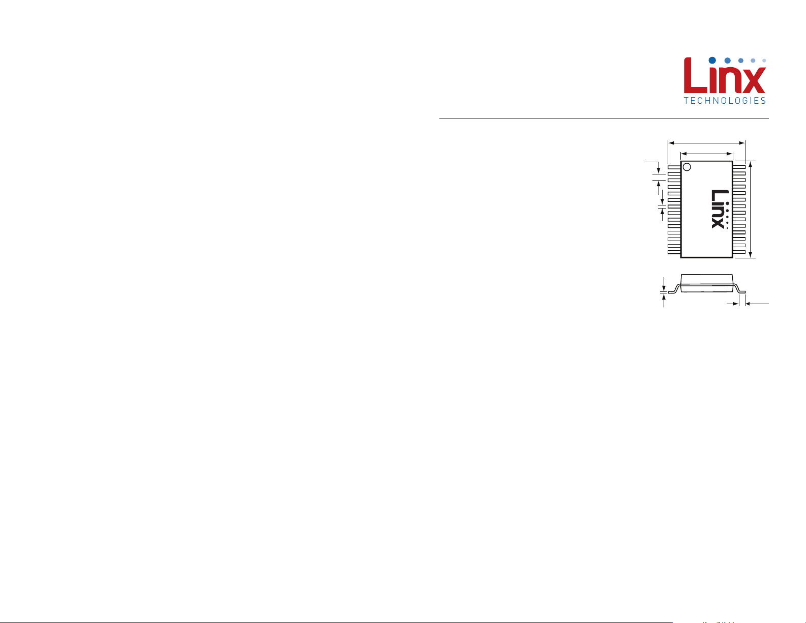
DS Series Encoder/Decoder
Data Guide
Description
The DS Series encoder/decoder is ideal for
remote control applications. It is used to
transfer the status of up to eight buttons or
contacts across a wireless link. Addressing is
accomplished by the logic state of 10 pins,
typically connected to DIP switches. The
encoder and decoder are in the same part,
selected by the state of one pin, which is a
benefit for volume purchasing and production.
0.026
(0.65)
0.015
(0.38)
0.323
(8.2)
0.220 (5.6)
LICAL-EDC-DS001
YYWWNNN
0.413
(10.5)
The DS Series also has two protocols built
into the same part, selected by the state of
a single pin. One is compatible with Holtek®
devices, such as the HT640 and HT658. The
0.010
(0.25)
Figure 1: Package Dimensions
0.037
(0.95)
other protocol is a serial data structure that is much more immune to noise
and edge jitter. This protocol offers much more range and reliability than the
Holtek® protocol while keeping the simple DIP-switch addressing.
The DS Series is configured through hardware, so no programming or
software is required. Housed in a tiny 28-pin SSOP package, DS Series
parts feature low supply voltage and current consumption.
Features
• 10 address lines
• 8 data lines
• 2.2 to 5.5V operating voltage
• Low supply current (250µA @ 3V
encoder, 400µA @ 3V decoder)
• Ultra-low 0.3µA standby current
• No programmer required
• Small SMD package
• Valid transmission indicator
Applications
• Door and Gate Openers
• Remote Device Control
• Car Alarms / Starters
• Home / Industrial Automation
• Remote Status Monitoring
• Lighting Control
– –
1
Revised 3/18/2015
Page 4
Electrical SpecicationsOrdering Information
Ordering Information
Part Number Description
LICAL-EDC-DS001 DS Series Encoder/Decoder
EVAL-xxx-DS DS Series Evaluation Kit
Encoder/Decoders are supplied in tubes of 18 pcs.
Figure 2: Ordering Information
Absolute Maximum Ratings
Absolute Maximum Ratings
Supply Voltage V
CC
Any Input or Output Pin −0.3 to V
Max. Current Sourced By Output Pins 25 mA
Max. Current Sunk By Output Pins 25 mA
Max. Current Into V
CC
Max. Current Out Of GND 300 mA
Operating Temperature −40 to +85 ºC
Storage Temperature −65 to +150 ºC
Exceeding any of the limits of this section may lead to permanent damage to the device.
Furthermore, extended operation at these maximum ratings may reduce the life of this
device.
Figure 3: Absolute Maximum Ratings
Warning: This product incorporates numerous static-sensitive
components. Always wear an ESD wrist strap and observe proper ESD
handling procedures when working with this device. Failure to observe
this precaution may result in module damage or failure.
−0.3 to +6.5 VDC
+ 0.3 VDC
CC
250 mA
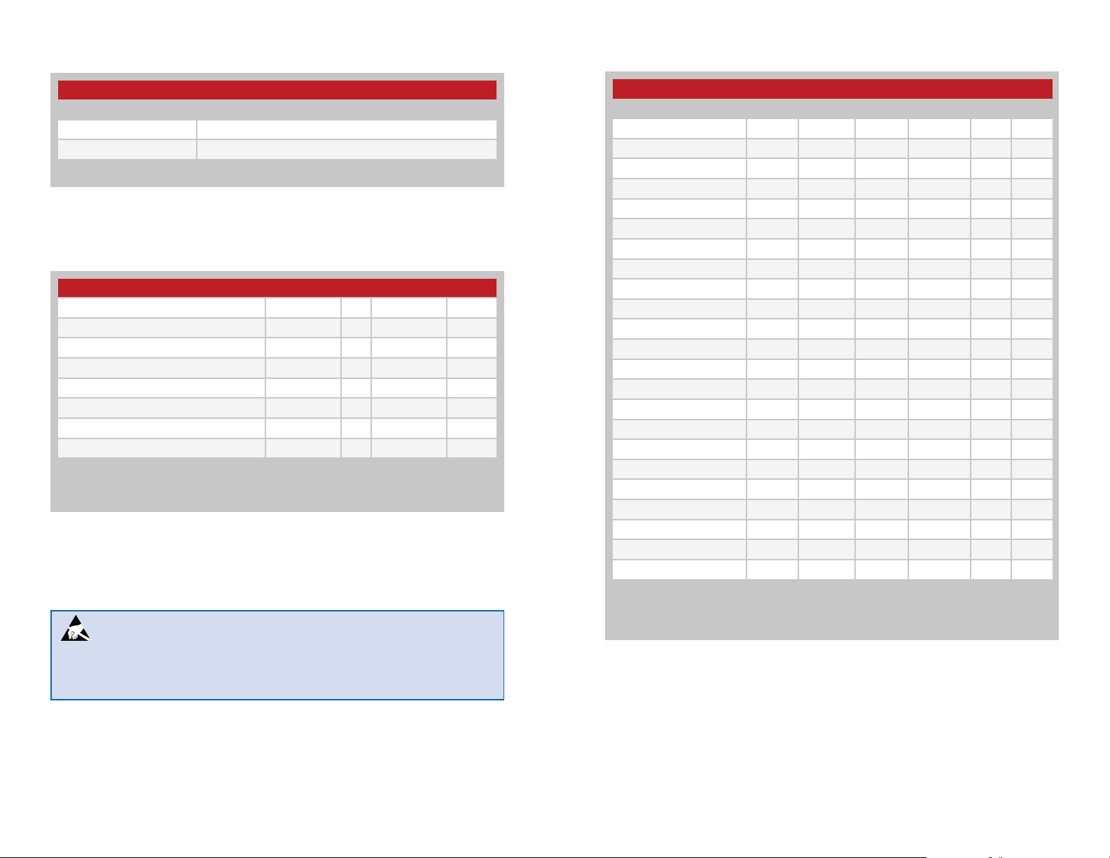
DS Series Encoder/Decoder Specifications
Parameter Symbol Min. Typ. Max. Units Notes
Operating Voltage V
Encoder Supply Current l
CC
CCENC
2.2 5.5 VDC
At 2.2V 200 µA 1
At 3.3V 250 µA 1
At 5.0V 400 µA 1
Decoder Supply Current l
CCDEC
At 2.2V 300 µA 1
At 3.3V 400 µA 1
At 5.0V 675 µA 1
Power-Down Current l
PDN
At 2.2V 0.3 µA
At 3.3V 0.3 µA
At 5.0V 0.4 µA
Input Low V
Input High V
Output Low V
Output High V
IL
IH
OL
OH
0.0 0.2 * V
0.8 * V
CC
CC
V
CC
0.0 0.6 V
VCC-0.7 V
CC
V 2
V 3
V
Input Sink Current 25 mA 4
Output Drive Current 25 mA 4
Operating Temp. Range −40 +85 ºC
Response Time
Holtek Protocol 135 ms
Serial Protocol 40 ms
1. Current consumption with no active loads.
2. For 3V supply, (0.15 x 3.0) = 0.45V max.
3. For 3V supply, (0.8 x 3.0) = 2.4V min.
4. Total current = 300mA
Figure 4: Electrical Specifications
– – – –
2
3
Page 5
Pin Assignments Pin Descriptions
A9
A8
A7
A6
A5
A4
A3
A2
A1
A0
28
27
26
25
24
23
22
21
20
19
18
17
16
15
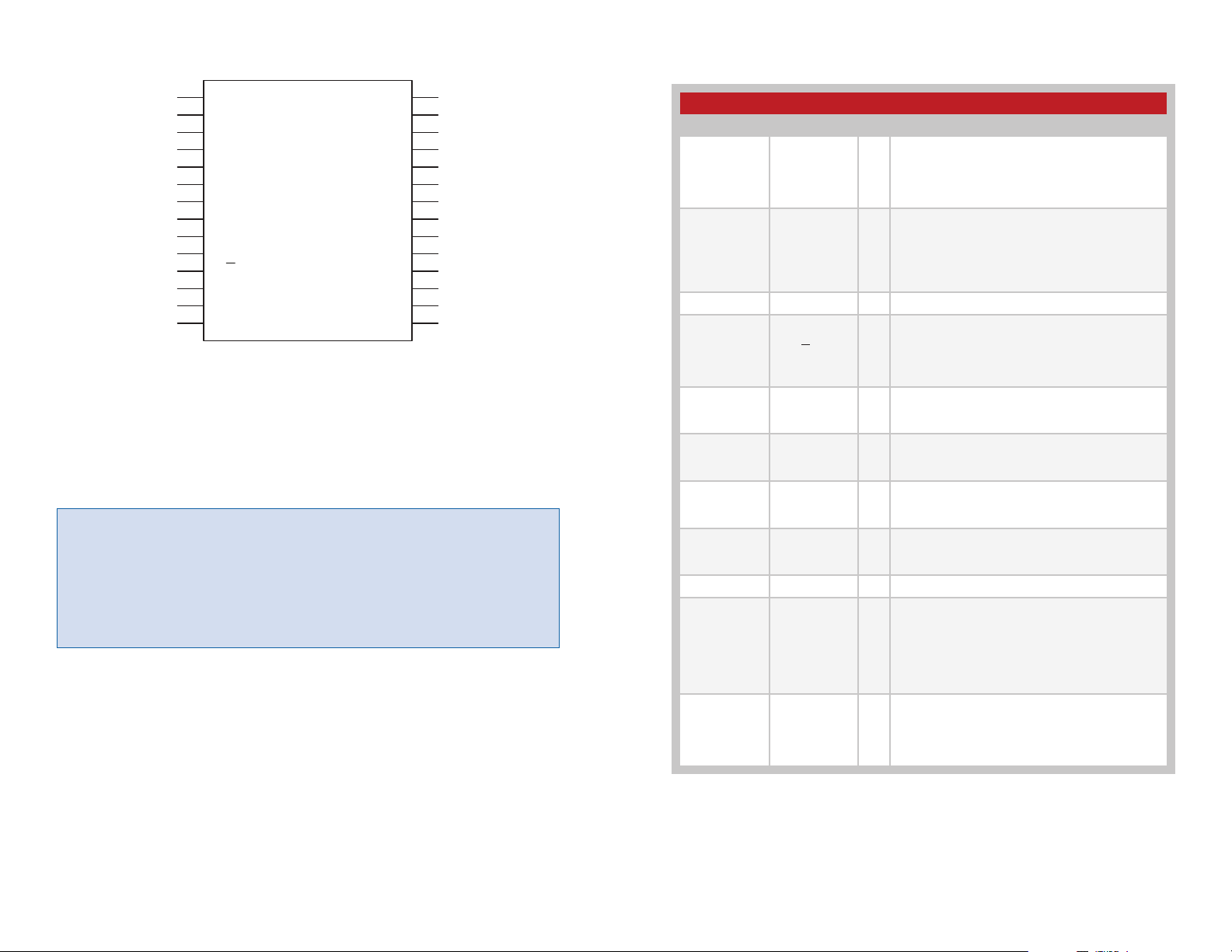
Pin Descriptions
Pin Number Name I/O Description
1 P_SEL I
2, 3, 4, 5, 6,
7, 9, 10
8, 19 GND Ground
11 E/D_SEL I
12 D_CFG I
13 A_CFG0 I
14 A_CFG1 I
15, 16, 17,
18, 21, 22,
23, 24, 25, 26
20 VCC This is the positive power supply.
27 TE/DIN I
28 DOUT/VT O
D0 – D7 I/O
A0–A9 I
1
P_SEL
2
D0
3
D1
4
D2
5
D3
6
D4
7
D5
8
GND
9
D6
10
D7
11
E/D_SEL
12
D_CFG
13
A_CFG0
14
A_CFG1
Figure 5: DS Series Encoder/Decoder Pinout (Top View)
DOUT/VT
TE/DIN
VCC
GND
Warning: None of the input lines have internal pull-up or pull-down
resistors. The input lines must always be in a known state (either
GND or VCC) at all times or the operation may not be predictable. The
designer must ensure that the input lines are never floating, either by
using external resistors, by tying the lines directly to GND or VCC, or by
use of other circuits to control the line state.
Protocol Selection. The state of this line
determines the data structure and protocol used
by the encoder / decoder. Pull low to use the
Holtek data structure, pull high to use the serial
structure.
Data Lines. When in Encoder Mode, the states
of these lines are captured when the TE line goes
high and are encoded for transmission. When in
Decoder Mode, these lines reproduce the states
of the encoder’s data lines upon reception of a
valid packet.
Encoder/Decoder Select. The state of this line
determines if the DS is an encoder or a decoder.
If the line is high, then the DS enters Encoder
Mode. If the line is low, then it enters Decoder
Mode. This line is checked once upon power up.
Data Line Configuration. Determines whether a
low on a data line is interpreted as a zero bit or
an open bit. See the Input Type Selection section.
Address Configuration 0. With A_CFG1,
determines the address bit type interpretation.
See the Input Type Selection section.
Address Configuration 1. With A_CFG0,
determines the address bit type interpretation.
See the Input Type Selection section.
Address Lines. The DS has ten address lines that
are used to set a local address.
When in Encoder Mode, this line is the Transmit
Enable line. When it is pulled high, the encoder
records the states of the data and address lines,
assembles them into a packet, and outputs the
packet on the DOUT line three times. When in
Decoder Mode, this line is the data input from the
receiver.
When in Encoder Mode, this line is the data
output that is connected to the transmitter. When
in Decoder Mode, this line is the Valid Transmit
indicator and goes high when a valid packet is
received.
Figure 6: DS Series Encoder/Decoder Pin Descriptions
– – – –
4
5
Page 6
Theory of Operation
The DS Series is a remote control encoder and decoder that offers two
protocols in one part based on the state of the P_SEL line. The first
protocol operates with the Holtek® HT640 encoder and HT658 decoder.
The second is a serial protocol that offers more noise immunity and faster
response time while keeping the simple addressing. The DS can operate
as either an encoder or decoder based on the state of the E/D_SEL line. It
does not operate as both simultaneously.
When set as an encoder it monitors the state of the TE line. When the line
is high the DS records the states of the data and address lines, assembles
them into a packet and outputs the packet three times. The data lines can
be connected to switches or contacts. The address lines can be set with
DIP switches or cut traces on a PCB.
When set as a decoder the DS receives packets and validates them. The
validation includes checking the bit timings and comparing the received
address to the local address line settings. Two matching packets must be
received consecutively. If the timings are good and the addresses match,
the DS sets its data lines to match the received states. These lines can be
connected to the application circuitry to be controlled.
When the TE/DIN line is low, the DS goes into a low power sleep mode.
Note: The input lines on the DS are not tri-state. They must be pulled
high or low and cannot be left floating. This is a key difference between
the DS and the Holtek® parts.
Setting the Address
The DS Series has ten address lines. This allows the formation of up to
1,022 (2
These lines may be hardwired or configured via a microprocessor, DIP
switch or jumpers. The receiver’s address line states must match the
transmitter’s exactly for a transmission to be recognized. If the addresses
do not match, then the decoder takes no action.
10
– 2) unique transmitter-receiver relationships.
Note: The DS decoder rejects packets with addresses set to all high
or all low. At least one address line must be different from the rest. The
encoder does transmit all addresses, but the decoder rejects packets
with all address lines set the same.
– – – –
6
Initial Operation
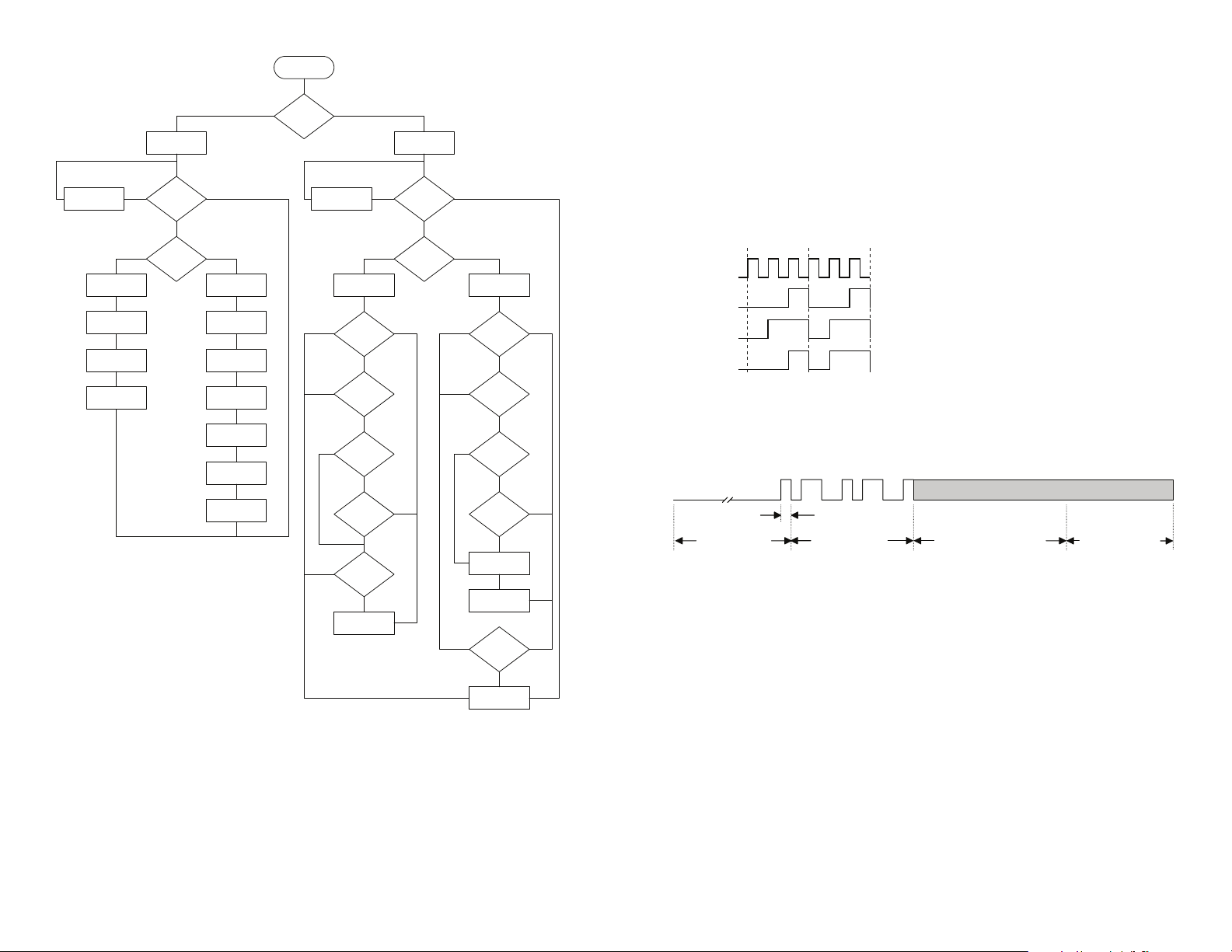
On power-up, the E/D_SEL line is tested to determine if the DS operates as
an encoder or a decoder. If the line is high, the DS enters Encoder Mode. If
low, it enters Decoder Mode. This is checked once on power-up. Once the
operating mode is selected, the data-line direction is set. In either mode a
rising edge on the TE/DIN line wakes the device from low-power sleep.
Encoder Mode
Once the DS enters Encoder Mode, it tests the state of the TE line. If it
is high, the P_SEL line is checked to determine which protocol to use.
Then the encoder records the states of the Data and Address lines and
assembles a packet. When the Holtek® protocol is selected, the DS
outputs the packet on the DOUT line three times. With the Serial protocol,
it sends two packets, checking the states of the data lines each time. The
second packet is the logical inversion of the first packet, ensuring a 50%
duty cycle, which is an advantage for FCC testing. The DS then checks the
state of the TE line again. It repeats this process for as long as the TE line is
high. Once it goes low, the DS goes to sleep until TE is pulled high.
Decoder Mode
When the DS enters Decoder Mode, it checks the state of the DIN line. If
it is high, the P_SEL line is checked to set which protocol is used and the
decoder receives the data. It compares the address in the received packet
to its local address lines. If they match, the data is stored and a second
packet is received. With the Holtek® protocol, the decoder compares the
two packets. If they match, the received data bits are output on the data
lines and the VT line is pulled high. This protocol compares each packet
with the previous one looking for a match. The serial protocol requires
two matching packets for initial activation, then updates the lines on each
subsequent packet. The DS then looks for the next packet on the DIN line.
With the Holtek® protocol, once no valid data is received (there is a
mismatch of address, data, or bit timings), the Data and VT lines are pulled
low and the DS goes to sleep until DIN is pulled high. The Serial protocol
holds the output states until a 130ms timer runs out.
The Holtek® protocol compares two packets and, if they match, sets the
outputs. If a data line is toggled during a transmission (D1 is activated while
D0 is already active) then the received packet does not match the previous
packet and the output lines are pulled low until the next packet arrives. This
causes all of the outputs to briefly cut out when a line is toggled. The serial
protocol uses a timer to prevent this cut out.
7
Page 7
Make pins D0-D7
inputs
Power On
EncoderDecoder
Is the
E/D_SEL line
high?
NOYES
Make pins D0-D7
outputs
Holtek Data and Packet Structure
The Holtek® encoders and decoders have tri-state input lines. They
recognize three distinct states: one, zero and open. A one bit is set when
the line is at VCC. A zero bit is set when the line is at ground. An open bit is
set when the line is not connected or floating.
Sleep
Wake on Interrupt
Set protocol to
Holtek
Read Data and
Address lines
Assemble packet
Output packet 3
times
NO
Is TE high?
YES
NO YES NO YES
Is P_SEL high?
Set protocol to
Serial
Read Data and
Address lines
Assemble packet
Output packet
Read Data and
Address lines
Assemble inverted
packet
Output packet
Sleep
Wake on interrupt
Set protocol to
Holtek
Valid data
NO
received?
YES
Address
NO
match?
YES
1st valid
NO
packet?
YES
2nd packet
received?
YES
Data match
NO
previous data?
YES
Activate outputs
and VT
NO
Is DIN high?
YES
Is P_SEL high?
NO
NO
NO
NO
Set protocol to
Serial
Valid data
received?
YES
Address
match?
YES
1st valid
packet?
YES
2nd packet
received?
YES
Activate outputs
and VT
Reset 130ms timer
130ms
timeout?
YES
Clear outputs and
VT
The Holtek® encoders and decoders use a pattern of two logic high pulses
and two logic low pulses for each bit. Two of the pulses are double sized
and the pattern indicates the type of bit. This is shown in Figure 8.
fosc/33
One
Zero
Open
Figure 8: Holtek® Protocol Input Interpretation
Each data packet consists of 6-bit pilot period (logic low), 2-bit SYNC
period, and 18-bit code period, as shown in Figure 9.
NO
Pilot Period
(6 bits)
Figure 9: Holtek® Protocol Packet Structure
NO
1/6 bit
Sync. Period Address Code Period Data Code Period
Figure 7: DS Series Encoder/Decoder Flowchart
– – – –
8
9
Page 8
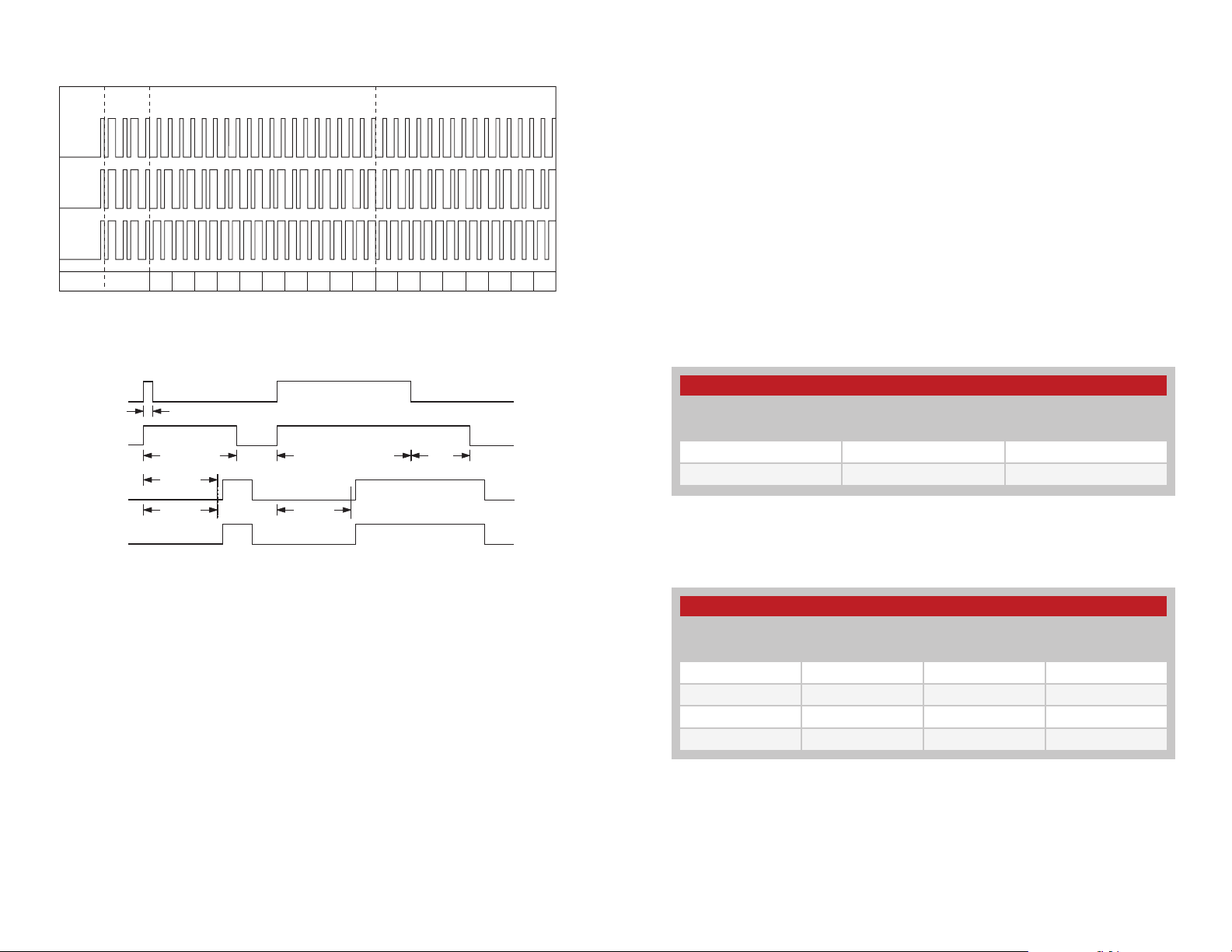
Example packets are shown in Figure 10 with all lines set in a specific state.
SYNC BITS
A&D BITS
PULLED TO
VCC
A&D BITS
OPEN
A&D Bits
PULLED TO
GND
SYNC
SYNC BITS A0 A1 A2 A3 A4 A5 A6 A7 A8 A9 D0 D1 D2 D3 D4 D5 D6 D7
PERIOD
Figure 10: Holtek® Protocol Timing
ADDRESS BITS DATA BITS
Figure 11 shows the timings associated with the Holtek® protocol.
Input Type Selection
The DS Series is designed to be operable with Holtek® encoders and
decoders, but there is one key condition. The Holtek® encoders and
decoders have tri-state input lines but the DS has bi-state lines. Tri-state
inputs are connected to ground for zero bits, VCC for one bits, or left
unconnected for open bits. Since the DS cannot match this operation
the D_CFG, A_CFG0 and A_CFG1 lines are provided to select the desired
interpretation. The settings must match on both ends.
Pulling D_CFG high configures the data inputs as one and zero. A high on
a data line is interpreted as a one bit and a low on the line is interpreted
as a zero bit. Pulling D_CFG low configures the data inputs as one and
open. A high on a data line is interpreted as a one bit and a low on the line
is interpreted as an open bit. The decoder outputs open data bits as logic
low. This is shown in Figure 12.
Encoder
Transmit
Enable
Encoder
Data Out
Decoder VT
Decoder
Data Out
2 Words
Figure 11: DS Series Timing
< 1 Word
3 Words
Check
Transmitted Continuously
Check
3 Words
D_CFG Configuration
Configuration Bit Interpretation
D_CFG High Low
0 One Open
1 One Zero
Figure 12: D_CFG Configuration
A_CFG0 and A_CFG1 are used to select the bit type for the address lines.
These are shown in Figure 13.
A_CFGO and A_CFG1 Configuration
Configuration Bit Interpretation
A_CFG1 A_CFG0 High Low
0 0 One Zero
0 1 One Open
1 0 Open Zero
1 1 One Zero
Figure 13: A_CFG0 and A_CFG1 Configuration
Products that need to operate with the older Holtek products need to
set these configuration lines according to how the Holtek® encoders and
decoders are implemented in the product.
– – – –
10
11
Page 9
Serial Data and Packet Structure
10
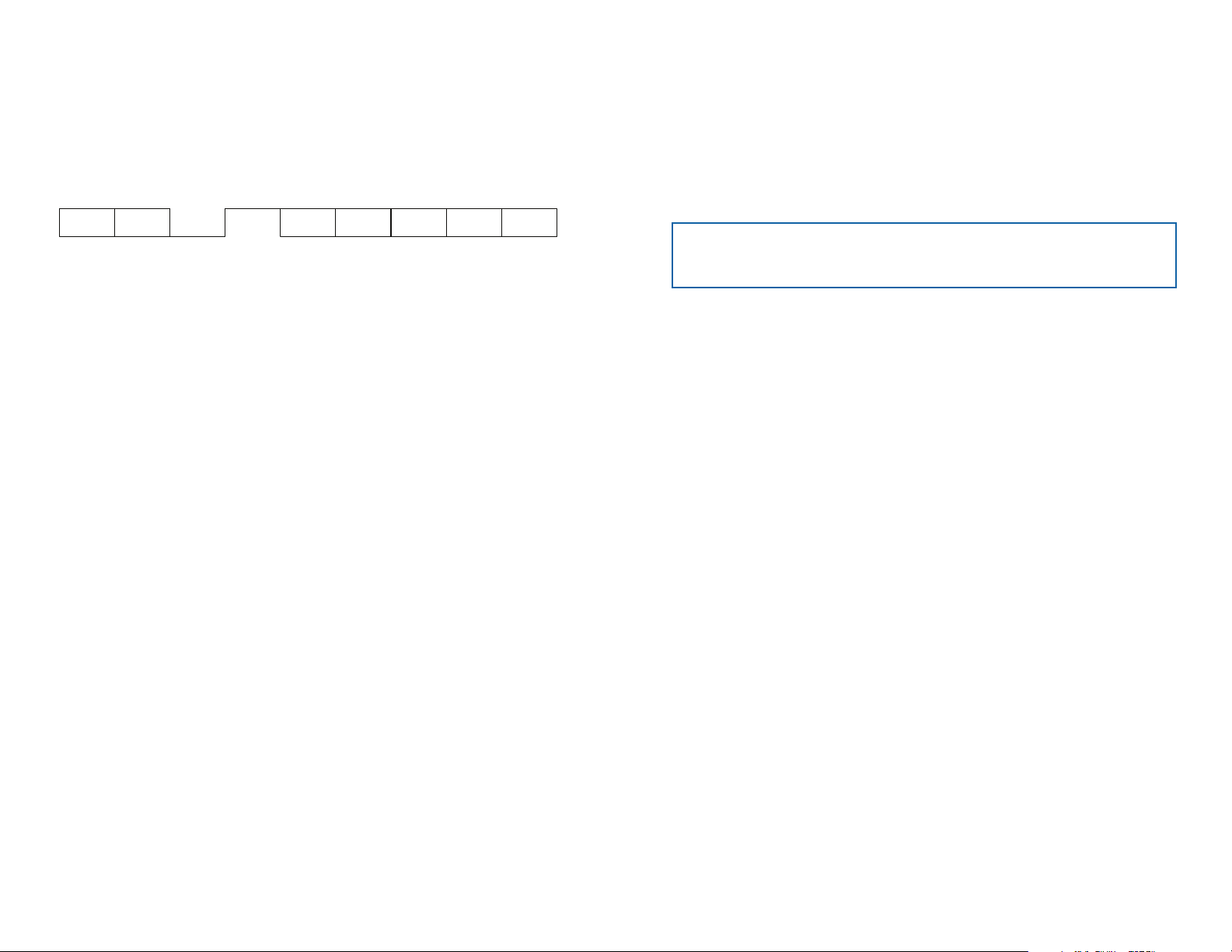
The serial protocol encodes the address and data lines as binary bits that
follow logic low and logic high voltage levels. The logic states of each line
are recorded and placed into bytes. A checksum is calculated on the bytes
and appended to the end of the packet. A preamble and a noise filter are
added to the front. The packet is shown in Figure 14.
2 Byte Preamble
0 1010 1010 10 1010 1010
Figure 14: Serial Protocol Packet Structure
1ms Low 1ms High
The bytes are output in serial fashion at 4,800bps. The DS outputs the
packet twice, with the second packet being the logical inversion of the first.
This ensures that the duty cycle of the data is always 50%. Adding in the
blanking period between packets lowers the duty cycle. This is important
for FCC certification where the transmitter output power level is a function
of the data duty cycle.
This protocol only uses binary states, so the D_CFG, A_CFG0 and A_CFG1
lines are ignored.
Sync Byte Addr. Bits 0-7Addr. Bits 8-9Data Bits 0-7 ChecksumNoise Filter
aa00 0000 1 0 dddd dddd 1 0 1001 1001 10 aaaa aaaa 1 0 cccc cccc 1
Operation with the Holtek® HT640 and HT658
The DS is fully compatible with the Holtek® HT640 encoder and the HT658,
and HT648L decoders. The primary operational difference is that the DS
Series has bi-state address lines (high or low) while the Holtek® parts have
tri-state lines (high, low or floating). Since these are distinct states for the
Holtek® parts, three configuration lines are used to select how the inputs
are interpreted. This accommodates most applications using the Holtek®
parts.
Note: Contact Linx for compatability with other Holtek® encoder/
decoder products.
The states of the A_CFG0 and A_CFG1 lines determine how the DS Series
interprets the states of its address lines. These lines allow for the use of any
two of Holtek®’s three states at a time. The states are outlined in Figure 13.
The state of the D_CFG line determines how the DS Series interprets the
states of its data lines when in Encoder Mode. This allows for the use of
any two of Holtek®’s three states at a time. The states are outlined in Figure
12.
The serial protocol is much more immune to bit edge jitter than the Holtek®
protocol. This gives much better range and performance within that range.
This also gives the DS better immunity to noise from motors, switching
power supplies, high current drivers and other noise sources.
This protocol updates the data line states on every packet. This, combined
with a faster data rate, give the serial protocol a much faster response time
than the Holtek® protocol (36.5ms typical compared to 135ms).
The serial protocol compares two packets as part of the data validation,
but also includes a timer that keeps the outputs stable in the case of
mismatched packets. This prevents the outputs from turning off at the
loss of one packet or when a data line is toggled while another one is
active. This helps prevent chattering of relays and other electro-mechanical
devices that are not designed for rapid switching. The outputs turn off after
130ms with no valid data.
– – – –
12
While the DS Series is not fully compatible with the Holtek® parts because
of the lack of tri-state lines, the use of the configuration lines allows most
applications to make a seamless transition to the DS.
13
Page 10
Encoder Typical Application
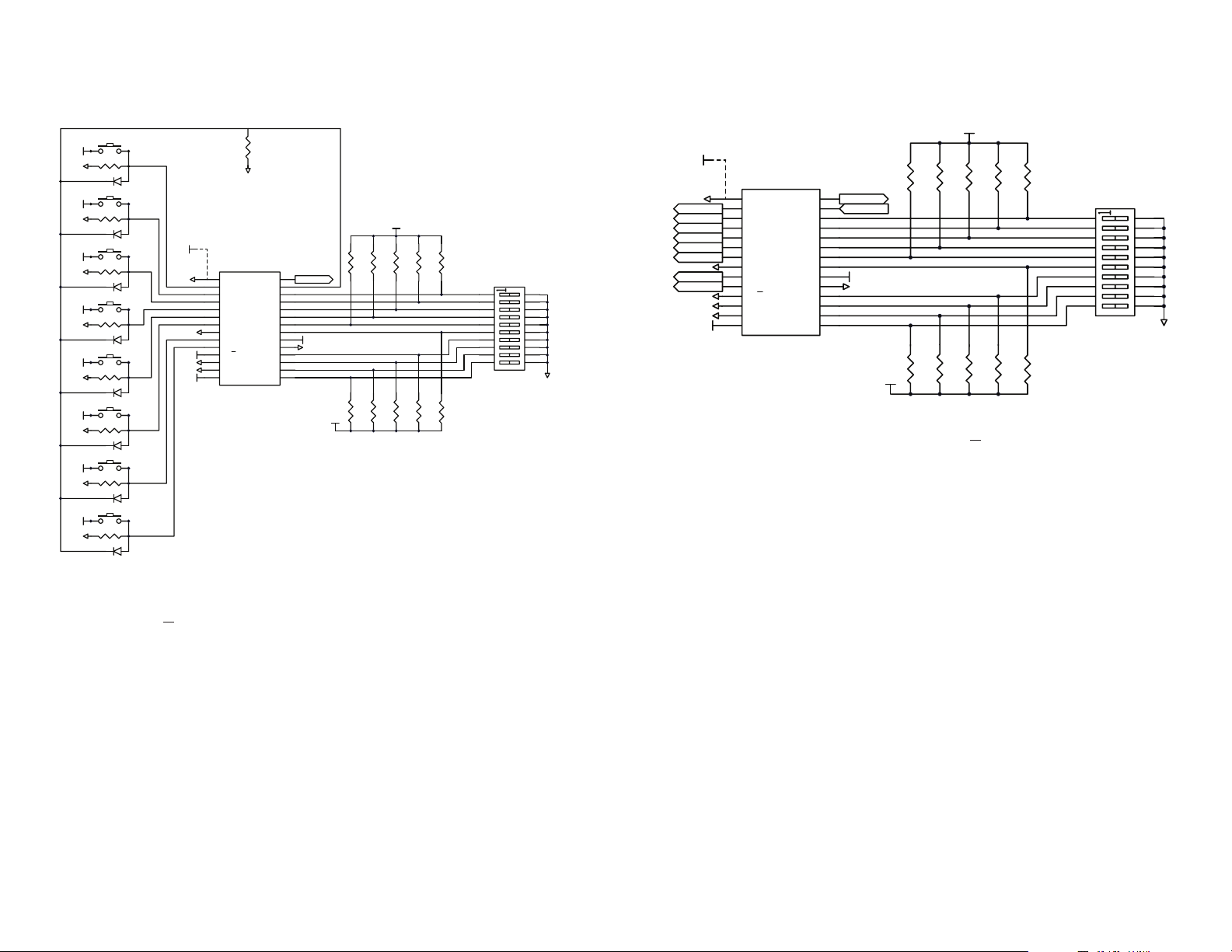
Figure 15 shows a circuit using the DS Series configured as a Holtek®
encoder. This configuration matches the Linx OEM products.
U1
1
2
D0
3
D1
4
D2
5
D3
6
D4
7
D5
8
GND
9
D6
10
D7
11
E/D_SEL
12
D_CFG
13
A_CFG0
A_CFG114A0
LICAL-EDC-DS001
GND
R18
100k
VT/DO
TE/DI
VCC
GND
VCC
R13
R14
R15
R16
100k
R10
100k
100k
R11
100k
R17
100k
R12
100k
SW1
1
2
3
4
5
6
7
8
9
10 11
100k
R8
100k
100k
R9
100k
28
TX_DATA
27
26
A9
25
A8
24
A7
23
A6
22
A5
21
A4
20
VCC
19
GND
18
A3
17
A2
16
A1
15
VCC
S0
VCC
R0 100k
GND
D0
S1
VCC
R1 100k
GND
VCC
GND
VCC
GND
VCC
GND
VCC
GND
VCC
GND
VCC
GND
D1
S2
R2 100k
D2
S3
R3 100k
D3
S4
R4 100k
D4
S5
R5 100k
D5
S6
R6 100k
D6
S7
R7 100k
D7
Serial
VCC
Holtek
GND P_SEL
GND
VCC
GND
GND
VCC
Figure 15: DS Series Typical Application as an Encoder
Decoder Typical Application
Figure 16 shows a circuit using the DS Series configured as a Holtek®
decoder. This configuration matches the Linx OEM products.
VCC
Serial
VCC
Holtek
GND
D0
D1
D2
D3
D4
D5
GND
D6
20
19
18
17
16
15
14
13
12
GND
D7
GND
GND
GND
VCC
U1
1
P_SEL
2
D0
3
D1
4
D2
5
D3
6
D4
7
D5
8
GND
9
D6
10
D7
11
E/D_SEL
12
D_CFG
13
A_CFG0
A_CFG114A0
LICAL-EDC-DS001
VT/DO
TE/DI
VCC
GND
28
VT
27
RX_DATA
26
A9
25
A8
24
A7
23
A6
22
A5
21
A4
20
VCC
19
GND
18
A3
17
A2
16
A1
15
Figure 16: DS Series Typical Application as a Decoder
The P_SEL line is set to Holtek® data. The E/D_SEL line is pulled low to
place the DS into decoder mode. The A_CFG0 and A_CFG1 lines are set
to give a high on an address line as an open bit and a low as a zero bit.
The address lines are bi-state, so they have to be high or low. They cannot
be floating. Resistors are used to pull the lines high and DIP switches pull
them low when on.
VCC
R13
100k
R8
100k
R14
100k
R9
100k
R15
100k
R10
100k
R16
100k
R11
100k
R17
100k
R12
100k
SW1
1
2
3
4
5
6
7
8
9
10 11
20
19
18
17
16
15
14
13
12
GND
The P_SEL line is set to Holtek® data (pulling it to Vcc selects the Serial
protocol. The E/D_SEL line is pulled high to place the DS into Encoder
Mode. The D_CFG is set so that a high on a data line is transmitted as a
one bit and a low on the line is transmitted as an open bit. The A_CFG0
and A_CFG1 lines are set to give a high on an address line as an open bit
and a low as a zero bit.
The data lines are bi-state, so they have to be high or low. They cannot be
floating. Resistors to ground pull the lines low and buttons pull the lines
high when pressed. Diodes are used to pull TE high when any button is
pressed without activating any other line. This way, pushing any button
causes the encoder to start outputting data.
The address lines are bi-state, so they have to be high or low. They cannot
be floating. Resistors pull the lines high and DIP switches pull them low.
– – – –
14
Pulling the P_SEL line to Vcc enables the serial protocol. The rest of the
application circuit is the same, though the D_CFG, A_CFG0 and A_CFG1
lines are ignored and can be tied to Vcc or GND with no affect on the
operation. They should not be left open.
15
Page 11
Recommended Pad Layout
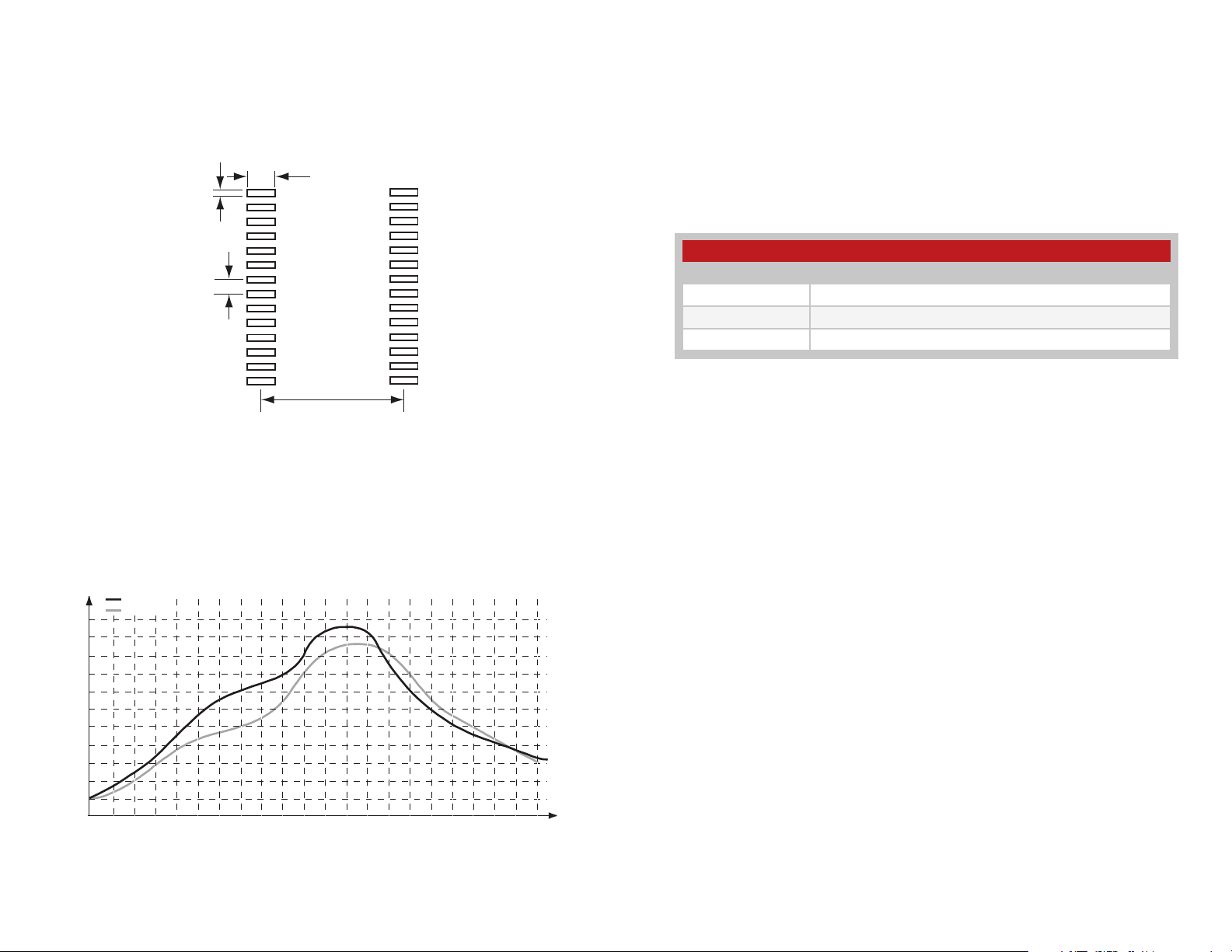
The DS Series encoder/decoder is implemented in a 28-pin Shrink Small
Outline Package (28-SSOP). The recommended layout dimensions are in
Figure 17.
0.071
(1.80)
0.016
(0.40)
0.026
(0.65)
0.283
(7.20)
Figure 17: Recommended Footprint
Production Guidelines
These surface-mount components are designed to comply with standard
reflow production methods. The recommended reflow profile is shown in
Figure 18 and should not be exceeded, as permanent damage to the part
may result.
Helpful Application Notes from Linx
It is not the intention of this manual to address in depth many of the issues
that should be considered to ensure that the modules function correctly
and deliver the maximum possible performance. As you proceed with your
design, you may wish to obtain one or more of the following application
notes which address in depth key areas of RF design and application of
Linx products. These application notes are available online at
www.linxtechnologies.com or by contacting Linx.
Helpful Application Note Titles
Note Number Note Title
AN-00300 Addressing Linx OEM Products
AN-00310 Encoder and Decoder Comparison
AN-00320 The Basics of Remote Control and Remote Keyless Entry
Figure 19: Helpful Application Notes
Lead-Free
275
250
225
200
175
150
125
100
75
TEMPERATURE (°C)
50
25
0
Sn / Pb
020406080 100 120 140 160 180 200 220 240 260 280 300 320
TIME (SECONDS)
Figure 18: Recommended Solder Profile
– – – –
16
260°C Max
240°C Max
340 360 380 420400
17
Page 12
Resources
Support
For technical support, product documentation, application notes, regulatory
guidelines and software updates, visit www.linxtechnologies.com
RF Design Services
For customers who need help implementing Linx modules, Linx offers
design services including board layout assistance, programming,
certification advice and packaging design. For more complex RF solutions,
Apex Wireless, a division of Linx Technologies, creates optimized designs
with RF components and firmware selected for the customer’s application.
Call +1 800 736 6677 (+1 541 471 6256 if outside the United States) for
more information.
Antenna Factor Antennas
Linx’s Antenna Factor division has the
industry’s broadest selection of antennas
for a wide variety of applications.
For customers with specialized needs,
custom antennas and design services are available along with simulations
of antenna performance to speed development. Learn more at
www.linxtechnologies.com.
by
Notes
– – – –
18
19
Page 13

Linx Technologies
159 Ort Lane
Merlin, OR, US 97532
Phone: +1 541 471 6256
Fax: +1 541 471 6251
www.linxtechnologies.com
Disclaimer
Linx Technologies is continually striving to improve the quality and function of its products. For this reason, we
reserve the right to make changes to our products without notice. The information contained in this Data Guide
is believed to be accurate as of the time of publication. Specifications are based on representative lot samples.
Values may vary from lot-to-lot and are not guaranteed. “Typical” parameters can and do vary over lots and
application. Linx Technologies makes no guarantee, warranty, or representation regarding the suitability of any
product for use in any specific application. It is the customer’s responsibility to verify the suitability of the part for
the intended application. NO LINX PRODUCT IS INTENDED FOR USE IN ANY APPLICATION WHERE THE SAFETY
OF LIFE OR PROPERTY IS AT RISK.
Linx Technologies DISCLAIMS ALL WARRANTIES OF MERCHANTABILITY AND FITNESS FOR A PARTICULAR
PURPOSE. IN NO EVENT SHALL LINX TECHNOLOGIES BE LIABLE FOR ANY OF CUSTOMER’S INCIDENTAL OR
CONSEQUENTIAL DAMAGES ARISING IN ANY WAY FROM ANY DEFECTIVE OR NON-CONFORMING PRODUCTS
OR FOR ANY OTHER BREACH OF CONTRACT BY LINX TECHNOLOGIES. The limitations on Linx Technologies’
liability are applicable to any and all claims or theories of recovery asserted by Customer, including, without
limitation, breach of contract, breach of warranty, strict liability, or negligence. Customer assumes all liability
(including, without limitation, liability for injury to person or property, economic loss, or business interruption) for
all claims, including claims from third parties, arising from the use of the Products. The Customer will indemnify,
defend, protect, and hold harmless Linx Technologies and its officers, employees, subsidiaries, affiliates,
distributors, and representatives from and against all claims, damages, actions, suits, proceedings, demands,
assessments, adjustments, costs, and expenses incurred by Linx Technologies as a result of or arising from any
Products sold by Linx Technologies to Customer. Under no conditions will Linx Technologies be responsible for
losses arising from the use or failure of the device in any application, other than the repair, replacement, or refund
limited to the original product purchase price. Devices described in this publication may contain proprietary,
patented, or copyrighted techniques, components, or materials. Under no circumstances shall any user be
conveyed any license or right to the use or ownership of such items.
©2015 Linx Technologies. All rights reserved.
The stylized Linx logo, Wireless Made Simple, WiSE, CipherLinx and the stylized CL logo are trademarks of Linx Technologies.
 Loading...