

Page 1

EVM-915-DTS
Data Guide
Page 2

Warning: Linx radio frequency ("RF") products may be used to
!
control machinery or devices remotely, including machinery or devices
that can cause death, bodily injuries, and/or property damage if
improperly or inadvertently triggered, particularly in industrial settings or
other applications implicating life-safety concerns. No Linx Technologies
product is intended for use in any application without redundancies
where the safety of life or property is at risk.
Table of Contents
1 Description
2 Ordering Information
2 Electrical Specications
3 Pin Assignments
The customers and users of devices and machinery controlled with
RF products must understand and must use all appropriate safety
procedures in connection with the devices, including without limitation,
using appropriate safety procedures to prevent inadvertent triggering by
the user of the device and using appropriate security codes to prevent
triggering of the remote controlled machine or device by users of other
remote controllers.
Do not use this or any Linx product to trigger an action directly
from the data line or RSSI lines without a protocol or encoder/
decoder to validate the data. Without validation, any signal from
another unrelated transmitter in the environment received by the
module could inadvertently trigger the action.
All RF products are susceptible to RF interference that can prevent
communication. RF products without frequency agility or hopping
implemented are more subject to interference. This module does not
have frequency agility built in.
Do not use any Linx product over the limits in this data guide.
Excessive voltage or extended operation at the maximum voltage could
cause product failure. Exceeding the reflow temperature profile could
cause product failure which is not immediately evident.
3 Pin Descriptions
4 PCB Footprint
4 Board Layout Guidelines
5 Schematic Diagram
6 Usage Guidelines for Regulatory Compliance
6 Additional Testing Requirements
7 Module Modication
7 Information to the user
8 Brazil Anatel Labeling Requirements
8 Product Labeling
9 Antenna Selection
10 Interference Considerations
11 Helpful Application Notes From Linx
11 Power Supply Requirements
Do not make any physical or electrical modifications to any Linx
product. This will void the warranty and regulatory and UL certifications
and may cause product failure which is not immediately evident.
Page 3
EVM-915-DTS RF
Data Guide
Description
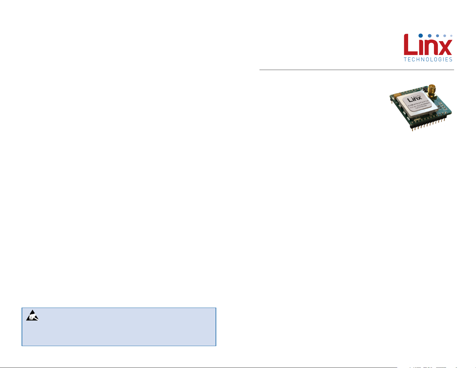
The EVM-915-DTS features the DTS Series
transceiver module in a FCC modular approved
solution. It is designed to greatly simplify
implementation of the DTS Series module into a
working design without the complications of FCC
testing.
Figure 1: EVM-915-DTS Module
The module combines a state-of-the art low power wireless transceiver
with a powerful multipoint-to-multipoint protocol controller to form a
transparent wireless communication solution capable of replacing wires in
almost any RS-232/422/485 application. With a 115dB link budget and
very low power operation modes, the DTS Series is excellent for AMR,
RFID, home automation, and any other application requiring long range
(<1500 feet, 457m line of sight) and long battery life.
Warning: This product incorporates numerous static-sensitive
components. Always wear an ESD wrist strap and observe proper ESD
handling procedures when working with this device. Failure to observe
this precaution may result in module damage or failure.
Features
• U.S FCC and Brazil ANATEL
Certified
• True UART to antenna solution
• 16-bit CRC error checking
• 100kbps max RF data rate
• 32 channels in DTS mode, 84 in
LP mode, North American version
• 19 unique channels in DTS mode,
52 unique channels in LP mode,
Brazilian version
Applications
• Direct RS-232/422/485 Wire
replacement
• Asset tracking
• Automated meter reading
– –
• Includes PHY and MAC protocol
• Low power Standby and Sleep
modes
• CSMA medium access control
• 115dB link budget in DTS mode
• 4 modes allow user to optimize
power/range
• 5 volt tolerant I/O
• 868–870MHz European version
available
• Industrial and/or home
automation
• Wireless sensors
• Remote data logging
1
Revised 3/18/2015
Page 4
Ordering Information
Pin Assignments
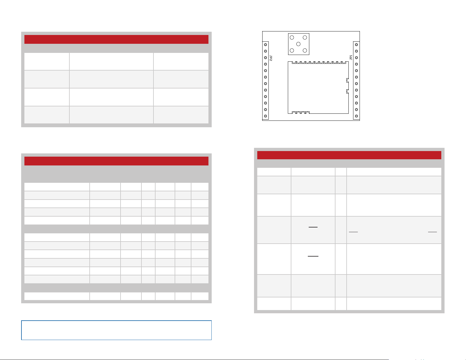
Ordering Information
Product Part No. Description Radiotronix Part No.
TRM-915-DTS Evaluation Module,
EVM-915-DTS-FCS
915MHz, Straight RP-SMA Connector,
Wi.232DTS-FCC-ST-R
FCC Approved
TRM-915-DTS Evaluation Module,
EVM-915-DTS-FCR
915MHz, Right Angle RP-SMA
Wi.232DTS-FCC-RA-R
Connector, FCC Approved
TRM-915-DTS Evaluation Module,
EVM-915-DTS-BRZ
915MHz, Right Angle RP-SMA
Wi.232DTSB-EVM-RA-R
Connector, Brazil Anatel Approved
TRM-915-DTS-BRZ Evaluation
EVM-915-DTS-BZS
Module, 915MHz, Straight RP-SMA
Wi.232DTSB-EVM-ST-R
Connector, Brazil Anatel Approved
Figure 2: Ordering Information
Electrical Specications
Electrical Specifications
Parameter Designation Min. Typ. Max. Units Notes
Power Supply
Operating Voltage V
Supply Current I
CC
CC
Receive 25 mA
Transmit, Po = 0dBm 35 mA
Transmit, Po = 13dBm 60 mA
Digital Interface
Output
Logic Low V
Logic High V
OL
OH
Input
Logic Low V
Logic High V
IL
IH
Environmental
Operating Temperature Range –40 85 °C
Figure 3: Electrical Specifications
Note: Please see the TRM-915-DTS data guide for complete information
about the module, detailed specifications and configuration commands.
4 12 VDC
0 0.4 VDC
2.5 V
CC
0 0.3*VCCVDC
0.7*V
CC
V
CC
VDC
VDC
1
2
3
4
5
6
7
8
9
10
11
12
Figure 4: DTS Series EVM Module Pin Assignments (Top View)
Pin Descriptions
Pin Descriptions
Pin Number Name I/O Description
1 VCC — Supply Voltage
2 RXD I
3 TXD O
4 CTS O
5 CMD I
6, 7, 8, 9, 10,
15, 16, 17,
18, 19, 20,
NC —
21, 22
11, 12, 13,
14, 23, 24
GND — Ground
Figure 5: DTS Series EVM Module Pin Descriptions
UART Receive Data Input. This is the input
line for the configuration commands as well
as data to be sent over the air.
UART Transmit Data Output. This is the
output line for the configuration command
responses as well as the data received over
the air.
UART Clear To Send, active low. This line
indicates to the host microcontroller when
the module is ready to accept data. When
CTS is high, the module is busy. When CTS
is low, the module is ready for data.
Command Input. This line sets the serial
data as either command data to configure
the module or packet data to be sent over
the air. Pull low for command data; pull high
for packet data.
No Electrical Connection. Do not connect
any traces to these lines.
24
23
22
21
20
19
18
17
16
15
14
13
– – – –
32
Page 5
PCB Footprint
1.50”
(38.10)
Schematic Diagram
VCCVCC
0.208”
0.05”
(1.27)
(5.28)
0.10”
(2.54)
Ø0.04” x 24
(1.02)
0.7”
(1.78)
1.38”
(35.05)
1 24
1.40”
0.05”
(1.27)
(35.56)
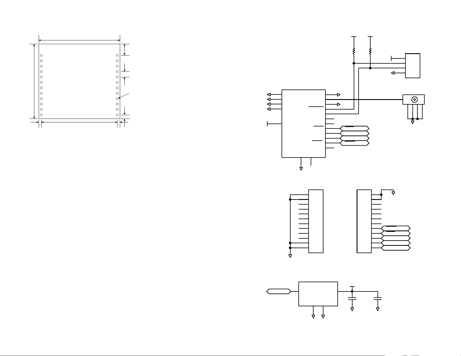
Figure 6: DTS Series EVM Module PCB Footprint
Board Layout Guidelines
The module’s design makes integration straightforward; however, it
is still critical to exercise care in PCB layout. Failure to observe good
layout techniques can result in a significant degradation of the module’s
performance. Grounding, filtering, decoupling, routing and PCB stack-up
are all important considerations for any RF design. Some basic design
guidelines are provided here.
The module should, as much as reasonably possible, be isolated from
other components on your PCB, especially high-frequency circuitry such as
crystal oscillators, switching power supplies, and high-speed bus lines.
When possible, separate RF and digital circuits into different PCB regions.
GND
GND
GND
GND
VCC
15
16
17
18
19
MOD1
GND
GND
GND
GND
VCC
GND
GND
ANT
GND
RESET
C2D
CTS
TXD
RXD
CMD
GND1NC
2
JP1
12
11
10
9
8
7
6
5
4
3
2
1
NC
NC
NC
14
13
12
11
10
9
8
7
6
5
4
3
GND
GND
CTS
TXD
RXD
CMD
R1
1K
JP2
12
11
10
R2
1K
VCC
GND
9
8
7
6
5
4
3
2
1
CMD
CTS
TXD
RXD
VIN
JP3
1
2
3
4
J1
GND
GND
Make sure internal wiring is routed away from the module and antenna and
is secured to prevent displacement.
Bypass caps should be low ESR ceramic types and located directly
adjacent to the pin they are serving.
In some instances, a designer may wish to encapsulate or “pot” the
product. Since such compounds can considerably impact RF performance
and the ability to rework or service the product, it is the responsibility of the
designer to evaluate and qualify the impact and suitability of such materials.
– – – –
GND
U1
VIN
1
IN
GND2GND
3.3V
T
GNDGND
Figure 7: DTS Series EVM Module Schematic
OUT
VCC
3
+
C1
GND
C2
GND
54
Page 6

Usage Guidelines for Regulatory Compliance
The EVM-915-DTS module is provided with a United States FCC and
Brazil ANATEL Modular Certification. This certification shows that the
module meets the requirements of FCC Part 15 and ANATEL Resolution
506 standards for an intentional radiator. The integrator does not need to
conduct any further testing under these rules provided that the following
guidelines are met:
• An approved antenna must be directly coupled to the module’s
RP-SMA connector through an approved coaxial extension cable.
• Alternate antennas can be used, but may require the integrator to
perform certification testing.
• The module must not be modified in any way. Coupling of external
circuitry must not bypass the provided connectors.
• End product must be externally labeled with “Contains FCC ID:
Q7V-3F090003X”.
• The end product’s user’s manual must contain an FCC statement
equivalent to that listed on page 7 of this data guide.
• The antenna used for this transceiver must not be co-located or
operating in conjunction with any other antenna or transmitter.
• The integrator must not provide any information to the end-user on
how to install or remove the module from the end-product.
Note: The integrator is required to perform unintentional radiator testing
on the final product per FCC sections 15.107 and 15.109.
Any changes or modifications not expressly approved by Linx Technologies
could void the user’s authority to operate the equipment.
Additional Testing Requirements
The modules have been tested for compliance as an intentional radiator,
but the integrator is required to perform unintentional radiator testing on
the final product per FCC sections 15.107 and 15.109. Additional productspecific testing might be required. Please contact the FCC regarding
regulatory requirements for the application. Ultimately is it the integrator’s
responsibility to show that their product complies with the regulations
applicable to their product.
Module Modication
The module must not be physically altered in any way. If any connections
are made to the modules that bypass the module pins, socket or antenna
connector, neither the FCC nor Anatel modular certification can be
inherited.
Information to the User
The following information must be included in the product’s user manual.
FCC / IC NOTICES
This product contains FCC ID: OJMTRM900TTA
This device complies with Part 15 of the FCC rules. Operation of this device is
subject to the following two conditions:
1. This device may not cause harmful interference, and
2. this device must accept any interference received, including interference that
may cause undesired operation.
This equipment has been tested and found to comply with the limits for a Class
B digital device, pursuant to Part 15 of the FCC Rules. These limits are designed
to provide reasonable protection against harmful interference in a residential
installation. This equipment generates, uses and can radiate radio frequency
energy and, if not installed and used in accordance with the instructions,
may cause harmful interference to radio communications. However, there is
no guarantee that interference will not occur in a particular installation. If this
equipment does cause harmful interference to radio or television reception, which
can be determined by turning the equipment off and on, the user is encouraged
to try to correct the interference by one or more of the following measures:
• Reorient or relocate the receiving antenna.
• Increase the separation between the equipment and receiver.
• Connect the equipment into an outlet on a circuit different from that to which
the receiver is connected.
• Consult the dealer or an experienced radio/TV technician for help.
Any modifications could void the user’s authority to operate the equipment.
– – – –
76
Page 7
Brazil Anatel Labeling Requirements
The Brazil version, the EVM-915-250-BZx, has been tested and complies
with the Anatel regulations for sale in Brazil. The following should be
included in the product’s documentation.
Este equipamento opera em caráter secundário, isto é, não tem direito à
proteção contra interferência prejudicial, mesmo de estações do mesmo
tipo, e não pode causar interferência a sistemas operando em caráter
primário.
Antenna Selection
Under FCC and ANATEL regulations, this radio transmitter may only
operate using an antenna of a type and maximum (or lesser) gain approved
for the transmitter by the FCC and ANATEL. To reduce potential radio
interference to other users, the antenna type and its gain should be so
chosen that the equivalent isotropically radiated power (e.i.r.p.) is not more
than that necessary for successful communication.
The EVM-915-250-FCx radio transmitter has been approved by the FCC
and the EVM-915-250-BZx has been approved by ANATEL to operate with
the antenna types listed in Figure 8 with the maximum permissible gain
and required antenna impedance for each antenna type indicated. Antenna
types not included in this list, having a gain greater than the maximum gain
indicated for that type, are strictly prohibited for use with this device.
Antennas
Linx Part Number Type Gain Impedance
ANT-916-CW-QW ¼ Wave Whip 1.84dBi 50Ω
ANT-916-CW-HW ½ Wave Dipole Helical 1.83dBi 50Ω
Figure 8: Antenna Selection
Product Labeling
The end product must be labeled to meet the FCC product label
requirements. It must have the below or similar text:
Contains FCC ID: OJMTRM900TTA
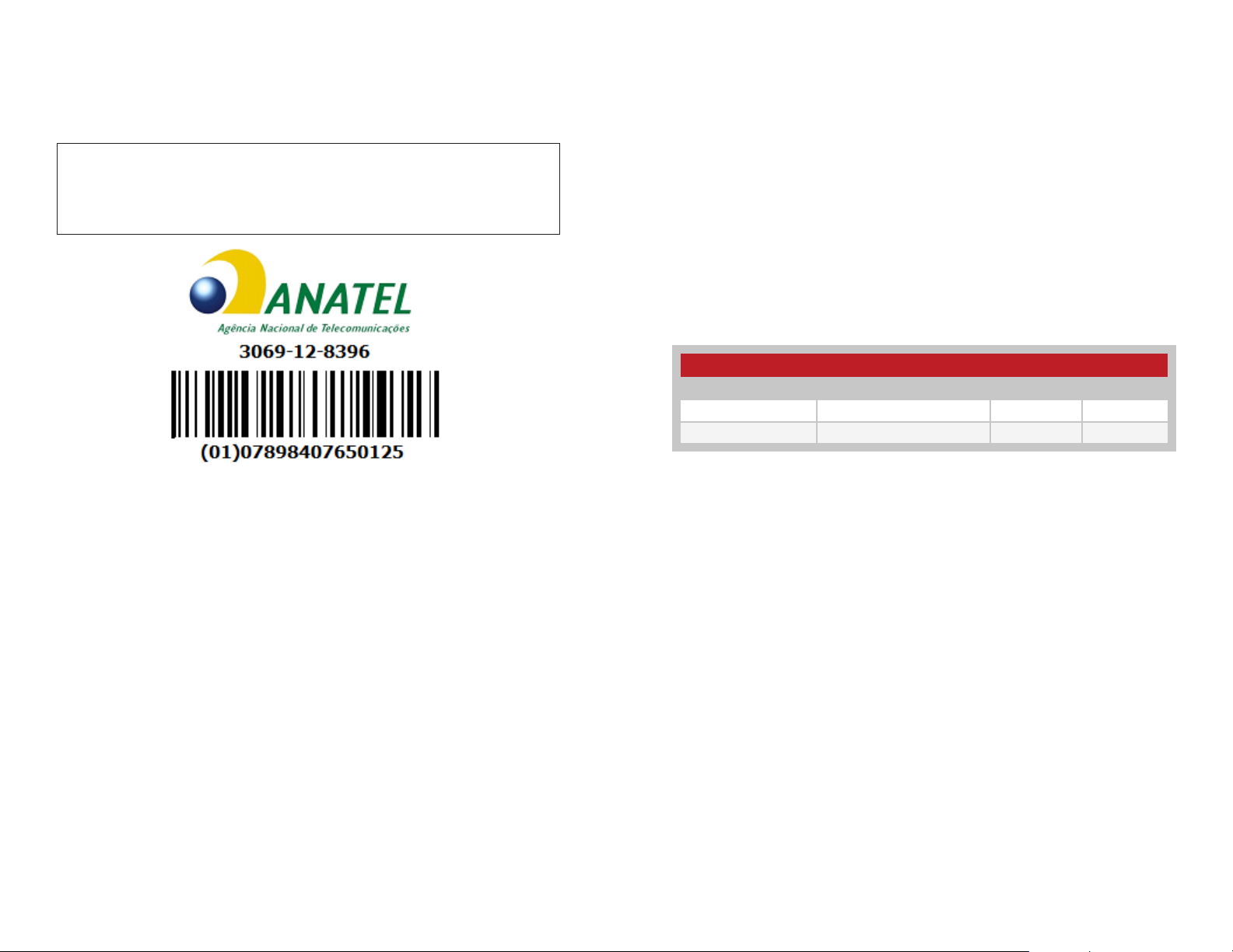
The Brazil version must contain:
Anatel: 3069-12-8396
The label must be permanently affixed to the product and readily visible to
the user. ‘‘Permanently affixed’’ means that the label is etched, engraved,
stamped, silkscreened, indelibly printed, or otherwise permanently marked
on a permanently attached part of the equipment or on a nameplate of
metal, plastic, or other material fastened to the equipment by welding,
riveting, or a permanent adhesive. The label must be designed to last
the expected lifetime of the equipment in the environment in which the
equipment may be operated and must not be readily detachable.
– – – –
When operating in DTS mode the module may be used with any of the
above antennas and maintain the requirements of the FCC grant. When
operating the module in LP mode, it must be used with the approved
¼ wave antenna. The module may not be used with the ½ wave dipole
antenna in LP mode.
An approved antenna must be directly attached to the module’s reversepolarity SMA connector in the final application to inherit the FCC and Anatel
modular certification.
98
Page 8
Interference Considerations
The RF spectrum is crowded and the potential for conflict with unwanted
sources of RF is very real. While all RF products are at risk from
interference, its effects can be minimized by better understanding its
characteristics.
Interference may come from internal or external sources. The first step
is to eliminate interference from noise sources on the board. This means
paying careful attention to layout, grounding, filtering and bypassing in
order to eliminate all radiated and conducted interference paths. For
many products, this is straightforward; however, products containing
components such as switching power supplies, motors, crystals and other
potential sources of noise must be approached with care. Comparing your
own design with a Linx evaluation board can help to determine if and at
what level design-specific interference is present.
External interference can manifest itself in a variety of ways. Low-level
interference produces noise and hashing on the output and reduces the
link’s overall range.
Helpful Application Notes from Linx
It is not the intention of this manual to address in depth many of the issues
that should be considered to ensure that the modules function correctly
and deliver the maximum possible performance. As you proceed with your
design, you may wish to obtain one or more of the following application
notes which address in depth key areas of RF design and application of
Linx products. These application notes are available online at
www.linxtechnologies.com or by contacting Linx.
Helpful Application Note Titles
Note Number Note Title
AN-00100 RF 101: Information for the RF Challenged
AN-00126 Considerations for Operation Within the 902–928MHz Band
AN-00130 Modulation Techniques for Low-Cost RF Data Links
AN-00140 The FCC Road: Part 15 from Concept to Approval
AN-00160 Considerations for Sending Data Over a Wireless Link
AN-00500 Antennas: Design, Application, Performance
AN-00501 Understanding Antenna Specifications and Operation
High-level interference is caused by nearby products sharing the same
frequency or from near-band high-power devices. It can even come from
your own products if more than one transmitter is active in the same area.
It is important to remember that only one transmitter at a time can occupy
a frequency, regardless of the coding of the transmitted signal. This type of
interference is less common than those mentioned previously, but in severe
cases it can prevent all useful function of the affected device.
Although technically not interference, multipath is also a factor to be
understood. Multipath is a term used to refer to the signal cancellation
effects that occur when RF waves arrive at the receiver in different phase
relationships. This effect is a particularly significant factor in interior
environments where objects provide many different signal reflection paths.
Multipath cancellation results in lowered signal levels at the receiver and
shorter useful distances for the link.
Figure 9: Helpful Application Notes
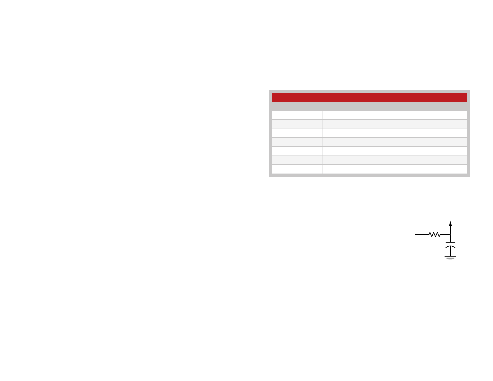
Power Supply Requirements
The transceiver incorporates a precision
low-dropout regulator which allows operation
over a wide input voltage range. Despite this
regulator, it is still important to provide a supply
Vcc IN
that is free of noise. Power supply noise can
significantly affect the module’s performance, so
providing a clean power supply for the module
should be a high priority during design.
Figure 10: Supply Filter
A 10Ω resistor in series with the supply followed by a 10μF tantalum
capacitor from Vcc to ground helps in cases where the quality of supply
power is poor (Figure 10). This filter should be placed close to the module’s
supply lines. These values may need to be adjusted depending on the
noise present on the supply line.
Vcc TO
MODULE
10Ω
+
10µF
– – – –
1110
Page 9

Linx Technologies
159 Ort Lane
Merlin, OR, US 97532
Phone: +1 541 471 6256
Fax: +1 541 471 6251
www.linxtechnologies.com
Disclaimer
Linx Technologies is continually striving to improve the quality and function of its products. For this reason, we
reserve the right to make changes to our products without notice. The information contained in this Data Guide
is believed to be accurate as of the time of publication. Specifications are based on representative lot samples.
Values may vary from lot-to-lot and are not guaranteed. “Typical” parameters can and do vary over lots and
application. Linx Technologies makes no guarantee, warranty, or representation regarding the suitability of any
product for use in any specific application. It is the customer’s responsibility to verify the suitability of the part for
the intended application. NO LINX PRODUCT IS INTENDED FOR USE IN ANY APPLICATION WHERE THE SAFETY
OF LIFE OR PROPERTY IS AT RISK.
Linx Technologies DISCLAIMS ALL WARRANTIES OF MERCHANTABILITY AND FITNESS FOR A PARTICULAR
PURPOSE. IN NO EVENT SHALL LINX TECHNOLOGIES BE LIABLE FOR ANY OF CUSTOMER’S INCIDENTAL OR
CONSEQUENTIAL DAMAGES ARISING IN ANY WAY FROM ANY DEFECTIVE OR NON-CONFORMING PRODUCTS
OR FOR ANY OTHER BREACH OF CONTRACT BY LINX TECHNOLOGIES. The limitations on Linx Technologies’
liability are applicable to any and all claims or theories of recovery asserted by Customer, including, without
limitation, breach of contract, breach of warranty, strict liability, or negligence. Customer assumes all liability
(including, without limitation, liability for injury to person or property, economic loss, or business interruption) for
all claims, including claims from third parties, arising from the use of the Products. The Customer will indemnify,
defend, protect, and hold harmless Linx Technologies and its officers, employees, subsidiaries, affiliates,
distributors, and representatives from and against all claims, damages, actions, suits, proceedings, demands,
assessments, adjustments, costs, and expenses incurred by Linx Technologies as a result of or arising from any
Products sold by Linx Technologies to Customer. Under no conditions will Linx Technologies be responsible for
losses arising from the use or failure of the device in any application, other than the repair, replacement, or refund
limited to the original product purchase price. Devices described in this publication may contain proprietary,
patented, or copyrighted techniques, components, or materials. Under no circumstances shall any user be
conveyed any license or right to the use or ownership of such items.
©2015 Linx Technologies. All rights reserved.
The stylized Linx logo, Wireless Made Simple, WiSE, CipherLinx and the stylized CL logo are trademarks of Linx Technologies.
 Loading...