

Page 1

DS Series
Basic Evaluation Kit
User's Guide
Page 2

Warning: Some customers may want Linx radio frequency (“RF”)
!
products to control machinery or devices remotely, including machinery
or devices that can cause death, bodily injuries, and/or property
damage if improperly or inadvertently triggered, particularly in industrial
settings or other applications implicating life-safety concerns (“Life and
Property Safety Situations”).
Table of Contents
1 Introduction
2 Ordering Information
2 DS Series Encoder Evaluation Board
NO OEM LINX REMOTE CONTROL OR FUNCTION MODULE
SHOULD EVER BE USED IN LIFE AND PROPERTY SAFETY
SITUATIONS. No OEM Linx Remote Control or Function Module
should be modified for Life and Property Safety Situations. Such
modification cannot provide sufficient safety and will void the product’s
regulatory certification and warranty.
Customers may use our (non-Function) Modules, Antenna and
Connectors as part of other systems in Life Safety Situations, but
only with necessary and industry appropriate redundancies and
in compliance with applicable safety standards, including without
limitation, ANSI and NFPA standards. It is solely the responsibility
of any Linx customer who uses one or more of these products to
incorporate appropriate redundancies and safety standards for the Life
and Property Safety Situation application.
Do not use this or any Linx product to trigger an action directly
from the data line or RSSI lines without a protocol or encoder/
decoder to validate the data. Without validation, any signal from
another unrelated transmitter in the environment received by the module
could inadvertently trigger the action.
All RF products are susceptible to RF interference that can prevent
communication. RF products without frequency agility or hopping
implemented are more subject to interference. This module does not
have a frequency hopping protocol built in.
3 DS Series Decoder Evaluation Board
4 Theory of Operation
4 Using the Kit
4 Selecting the Protocol
5 Setting the Address
5 Conguring the Holtek Protocol
6 Development Using the Prototyping Area
6 Range Testing
8 Using the Boards as a Design Reference
8 About Antennas
8 In Closing
9 Resources
10 DS Series Encoder Evaluation Board Schematic
11 DS Series Decoder Evaluation Board Schematic
Do not use any Linx product over the limits in this data guide.
Excessive voltage or extended operation at the maximum voltage could
cause product failure. Exceeding the reflow temperature profile could
cause product failure which is not immediately evident.
Do not make any physical or electrical modifications to any Linx
product. This will void the warranty and regulatory and UL certifications
and may cause product failure which is not immediately evident.
Page 3
DS Series Basic Evaluation Kit
User's Guide
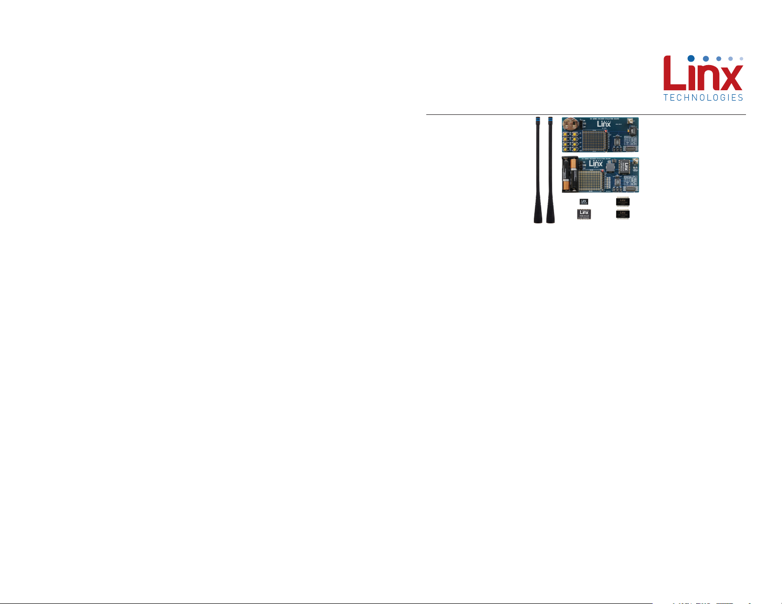
Figure 1: DS Series Basic Evaluation Kit
Introduction
The DS Series encoder / decoder offers a simple, efficient and
cost-effective method of adding wireless remote control capabilities to any
product. The Basic Evaluation Kit gives a designer all the tools necessary
to correctly and legally incorporate the DS Series encoder / decoder
into an end product. This guide shows how to take full advantage of the
development boards included with the system. The evaluation kit serves
several important functions:
• Rapid Evaluation: The boards allow the performance of the DS Series
encoder / decoder to be evaluated quickly in a user’s environment.
• Prototype Development: An on-board prototyping area allows for the
development of applications directly on the development board.
All signal lines are available on a header for easy access.
• Range Testing: Using the on-board encoders and decoders to generate
a simplex transmission, a pair of development boards can be used to
evaluate the range performance of the modules.
• Design Benchmark: The boards provide a known benchmark against
which the performance of a custom design may be judged.
This kit includes 4 DS Series encoders / decoders*, 2 LR Series
transmitters*, 2 LR Series receivers*, 2 development boards, 2 CW Series
antennas, 1 CR2032 battery, 2 AAA batteries and full documentation.
*Two DS Series encoders / decoders, 1 LR Series transmitter and 1 LR Series receiver are
soldered to the boards, the rest are for use on prototypes.
– –
1
Revised 3/18/2015
Page 4
Ordering Information
DS Series Decoder Evaluation Board
Ordering Information
Part Number Description
EVAL-xxx-DS DS Series Basic Evaluation Kit
LICAL-EDC-DS001 DS Series Encoder/Decoder
xxx = 315, 418 (Standard), 433MHz
Figure 2: Ordering Information
DS Series Encoder Evaluation Board
1
4
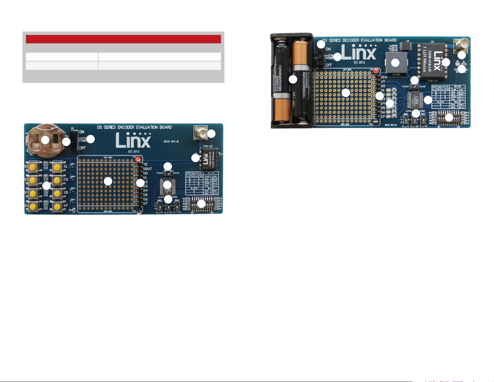
Figure 3: DS Series Encoder Evaluation Board
2
1. Battery – 3VDC (use a CR2032-style battery only)
2. Power Switch
3. Power On Indicator LED
4. Momentary Pushbuttons
5. Prototyping Area
6. Breakout Header
7. Reverse-Polarity SMA Antenna Connector
8. LR Series Transmitter Module
9. DS Series Encoder / Decoder
10. Protocol Select Switch
11. Holtek Protocol Configuration Switches
12. Address Configuration DIP Switch
3
5
6
10
9
11
2
3
1
4
7
8
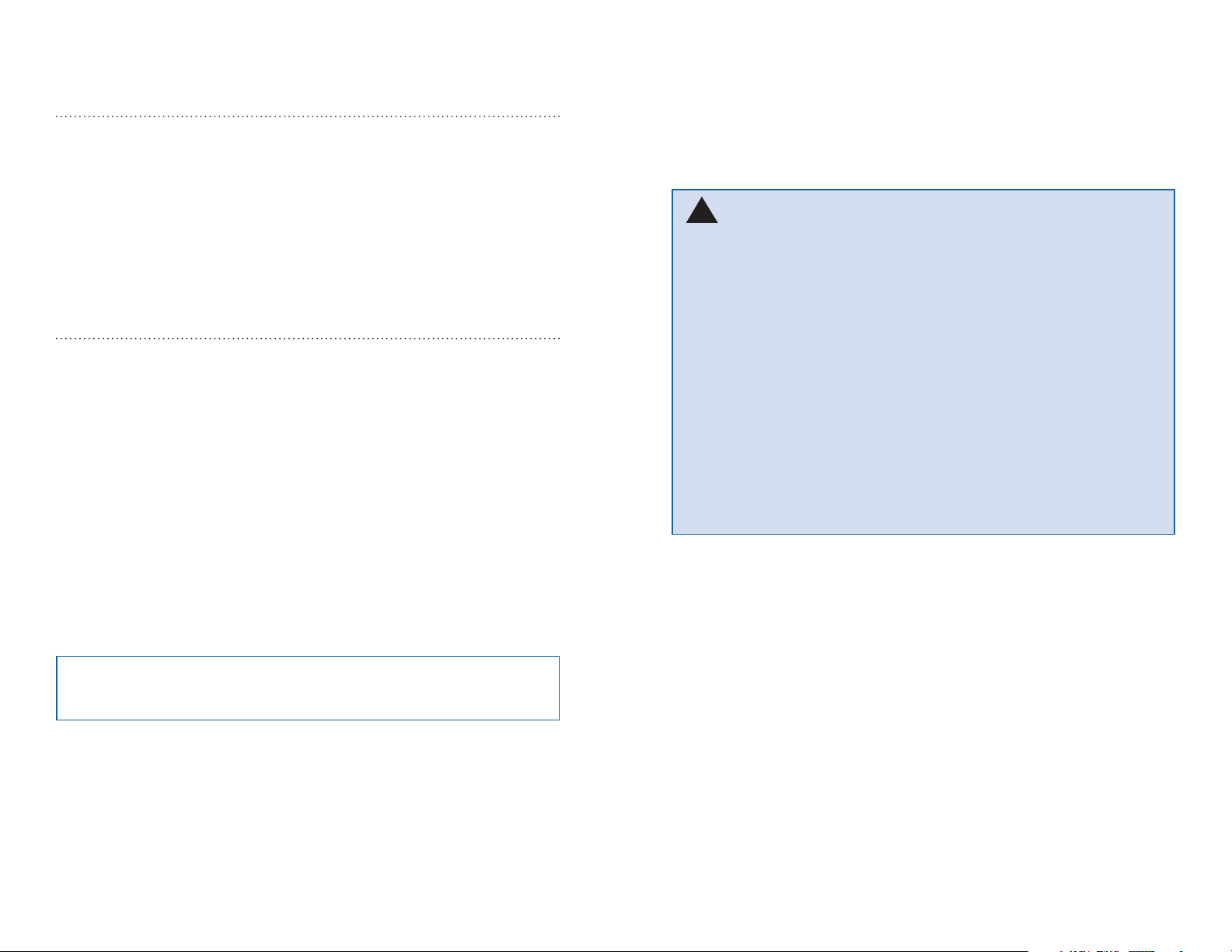
Figure 4: DS Series Decoder Evaluation Board
1. Battery – 3VDC (use 2 AAA style batteries)
2. Power Switch
10
11
5
9
7
12
8
6
14
13
3. Power On Indicator LED
4. Prototyping Area
5. Breakout Header
6. LR Series Receiver Module
12
7. DS Series Encoder / Decoder
8. Reverse-Polarity SMA Antenna Connector
9. LEDs – D1–D7
10. Buzzer – D0
11. Protocol Select Switch
12. Holtek Configuration Switches
13. Address Configuration DIP Switch
14. Valid Transmission Received LED
– – – –
2 3
Page 5
Theory of Operation
Encoder Evaluation Board
The transmitter board is powered by an on-board 3V CR2032 lithium
battery. It has eight SPST pushbutton switches, the states of which
are encoded into a data stream using the DS Series as an encoder. If a
switch is closed, the transmitter is enabled while the encoder captures the
pushbutton states for encoding and transmission. Buttons S0 (D0) is used
to activate a buzzer on the receiver board while the rest of the buttons
activate LEDs. All of the data lines are wired out to the header to the right
of the prototyping area and can be accessed for use with other switches,
contacts or microcontrollers.
Decoder Evaluation Board
The receiver board is powered by two AAA batteries. The data recovered
by the LR Series receiver is decoded using the DS Series as a decoder,
and the data line outputs are updated to match the states of the data line
inputs (or pushbuttons) on the transmitter board. To demonstrate this, one
data line is used to activate a buzzer while the other seven are used to
drive LEDs. This board also has a prototyping area with all of the receiver
and decoder lines brought out to a header.
Using the Kit
Using the kit is straightforward. Simply attach the antennas, turn on the
power, and press buttons on the transmitter board. When S0 is pressed,
the buzzer sounds; when S1–S7 are pressed, the LEDs turn on. When
any button (S0–S7) is pressed on the transmitter board, the corresponding
decoder output (D0–D7) is active high (VCC) on the prototyping header.
Note: All switches (address, protocol select and Holtek configuration)
must match on both the encoder and decoder boards.
Setting the Address
The address is made of ten inputs from the DIP switch, resulting in 1,022
10
(2
– 2) possible combinations. It’s important to remember that all switches
placed on or off are not valid addresses and are ignored. At least one input
must be different from the rest. Both the encoder and decoder board must
have matching addresses.
Warning: When designing remote control applications, it is very
!
important to use unique addressing between devices. This eliminates
opportunities for accidental triggering of unintentional devices within
range. For example, if next door neighbors have matching addresses
for their garage doors, each person would open both garage doors
when transmitting from a single remote controller. Likewise, suppose a
person shouts “John” in a room full of people. Each person named John
will respond. However, if the person shouts “John Smith”, only people
with the first same and last name will respond. For this reason it is very
important to set the address to a unique configuration.
Note: The DS Series has 10 address inputs which can be set to over a
thousand combinations. It is extremely important to mix up the address
logic, making the address more likely to be unique. Simple addressing
schemes, such as the first 9 address pins set to the same logic and the
10th address pin being inverted is NOT recommended.
Conguring the Holtek Protocol
The Holtek configuration switches are only necessary when using the
Holtek protocol; they can be ignored when using the Serial protocol. These
switches determine the Data and Address bit types for the Holtek protocol.
It’s important that the encoder and decoder boards have matching
configurations. See the DS Series Data Guide for further details.
Selecting the Protocol
The DS Series encoder / decoder offers two over-the-air protocols. The
Holtek selection is used when communicating with other Holtek devices.
The serial selection offers a much more reliable protocol to allow better
range and response time. See the DS Series Data Guide for more details.
– – – –
4 5
Page 6

Development Using the Prototyping Area
In addition to their evaluation functions, the boards may also be used for
product development. They feature a prototyping area to facilitate the
addition of application-specific circuitry. This area has a connection to
VCC at the top and ground at the bottom that can be used to power any
circuitry that is added.
Note: The CR2032-style battery on the transmitter board has very low
current capacity with, only about 3mA available for external circuitry. If
added circuitry requires a higher current, the battery must be removed
and the board powered from an external source.
The holes are plated and set at 0.1” on center with a 0.04” diameter,
making it easy to add most industry-standard SIP and DIP packages to the
board.
is normal and can result from other interfering sources or fluctuating signal
levels due to multipath. Multipath results in cancellation of the transmitted
signal as direct and reflected signals arrive at the receiver at differing times
and phases. The areas in which this occurs are commonly called “nulls”
and simply walking a little further usually restores the signal. If this does not
restore the signal, then the maximum effective range of the link has been
reached.
Since the evaluation boards are intended for use by design engineers,
they are not FCC certified. The transmitter has been set to approximate
legal limits by resistor R1 so that the range test results will approximate the
results from a well-designed, certified product. For applications where Part
15 limits are not applicable or output levels can be legally raised due to
protocol duty cycle, R1 can be changed according to the Output Power vs.
LADJ Resistance graph in the LR Series Transmitter Module Data Guide.
On the encoder board, the Transmit Enable (TE), Data Output (DOUT) and
data lines (D0–D7) from the encoder have been wired out to a row of plated
holes on the right side of the prototyping area. On the receiver board, the
Data In (DIN), the Valid Transmission (VT) and the data lines (D0–D7) from
the decoder have been wired out. This allows easy access to connect
external circuitry to the encoder and decoder. Data line D0 is connected to
the buzzer; D1–D7 and VT are connected to LEDs.
Range Testing
Several complex mathematical models exist for determining path loss in
many environments. These models vary as the transmitter and receiver are
moved from indoor operation to outdoor operation. Although these models
can provide an estimation of range performance in the field, the most
reliable method is to simply perform range tests using the transmitter and
receiver in the intended operational environment.
Basic range testing can be performed with the transmitter and receiver
evaluation boards. To prepare the board for range testing, turn it on
by switching the power switch to the ON position. Pressing S0 on the
transmitter activates the buzzer on the receiver board. For continuous
transmit, connect D0 to VCC. This allows the designer to turn on the
transmitter and walk with the receiver.
To achieve maximum range, keep objects such as your hand away from
the antenna and ensure that the antenna on the transmitting board has a
clear and unobstructed line-of-sight path to the receiving board. Range
performance is determined by many interdependent factors. If the range
you are able to achieve is significantly less than specified by Linx for the
products you are testing, then there is likely a problem with either the board
or the ambient RF environment in which the board is operating. First, check
the battery, switch positions, and antenna connection. Next, measure
the receiver’s RSSI voltage with the transmitter turned off to determine
if ambient interference is present. If this fails to resolve the issue, please
contact Linx technical support.
As the maximum range of the link in an area is approached, it is not
uncommon for the signal to cut in and out as the transmitter moves. This
– – – –
6 7
Page 7

Using the Boards as a Design Reference
The basic evaluation boards included in this kit are very simple, yet they
illustrate some important techniques that should be incorporated into the
board layout. The module’s mounting pads extend slightly past the edge of
the part. This eases hand assembly and allows for better heat conduction
under the part if rework is necessary. A full ground plane fill is placed on the
bottom of the board. This ground plane serves three important purposes:
First, since a quarter-wave antenna is employed, the ground plane is
critical to serve as a counterpoise (please see Application Note AN-00500
“Antennas: Design, Application, and Performance” for details on how a
ground plane affects antenna function).
Second, a ground plane suppresses the transfer of noise between stages
of a product as well as unintentional radiation of noise into free space.
Third, a ground plane allows for the implementation of a microstrip feed
between the module and the antenna. The term microstrip refers to a PCB
trace running over a ground plane that is designed to serve as a 50-ohm
transmission line. See the LR Series data guide or the calculator available
on our website for details on microstrip calculations.
About Antennas
The choice of antennas is one of the most critical and often overlooked
design considerations. The range, performance, and legality of an RF link
are critically dependent upon the type of antenna employed. Linx offers
a variety of antenna styles that can be considered for a design. Included
with your kit are CW Series connectorized whip antennas that should be
connected prior to using the kit. Despite the fact that the antenna is not
centered on the board’s ground plane, it exhibits a VSWR of <1.7 and
suitably demonstrates the module’s best practical performance.
Resources
Support
For technical support, product documentation, application notes, regulatory
guidelines and software updates, visit www.linxtechnologies.com
RF Design Services
For customers who need help implementing Linx modules, Linx offers
design services including board layout assistance, programming,
certification advice and packaging design. For more complex RF solutions,
Apex Wireless, a division of Linx Technologies, creates optimized designs
with RF components and firmware selected for the customer’s application.
Call +1 800 736 6677 (+1 541 471 6256 if outside the United States) for
more information.
Antenna Factor Antennas
Linx’s Antenna Factor division has the
industry’s broadest selection of antennas
for a wide variety of applications.
For customers with specialized needs,
custom antennas and design services are available along with simulations
of antenna performance to speed development. Learn more at
www.linxtechnologies.com.
by
In Closing
Here at Linx, “Wireless Made Simple” is more than just our motto, it is our
commitment. A commitment to the highest caliber of product, service,
and support. That is why, should you have questions or encounter any
difficulties using the evaluation kit, you’ll be glad to know many resources
are available to assist you. First, check carefully for the obvious, then
visit our website at www.linxtechnologies.com or call +1 541 471 6256
between 7AM and 5PM Pacific Time to speak with an application engineer.
– – – –
8 9
Legal Notice: All Linx kits and modules are designed in keeping with
high engineering standards; however, it is the responsibility of the user to
ensure that the products are operated in a legal and appropriate manner.
The purchaser understands that legal operation may require additional
permits, approvals, or certifications prior to use, depending on the
country of operation.
Page 8
ANT1
DS Series Encoder Evaluation Board Schematic DS Series Decoder Evaluation Board Schematic
S9
VCC
C1
10uF
+
VCC
ANT1
CONREVSMA001
1
GND
VCC
TE
5
6
8
VCC7PDN
GND
GND1DATA IN2GND3LADJ/VCC
U1
GND
VCC
4
GND
R1
620 ohm
D1
GND
RF
RF OUT
TXM-xxx-LR
GND
B1
R2
POWER GREEN
2-5
BAT-HLD-001
GND
620 ohm
GND
GND
TE
A9
27
28
TE/DIN
DOUT/VT
P_SEL1D02D13D24D35D46D57GND8D69D710E/D_SEL11D_CFG12A_CFG013A_CFG1
U2
D0D1D2D3D4D5D6
P_SEL
A[0..9]
VCC
1
123456789
J1
D0D1D2D3D4D5D6
TE
DOUT
VCC
A4A5A6A7A8
20A421A522A623A724A825A926
VCC
GND
TP11TP2
GND
A3
18
19
GND
D7
D_CFG
VCC
GND
10
HEADER 10
D7
A0A1A2
A015A116A217A3
LICAL- EDC-DS001
14
A_CFG0
A_CFG1
R10
100K
DP2
DP1
1
231
D0D1D2D3D4D5D6
S0S1S2S3S4S5S6
D[0..7]
VCC
R12100K
R9 100K
R7 100K
D0D1D2D3D4D5D6
231
R14100K
GND
DP3
R16100K
231
R18100K
R20100K
BZ1
VCC
1
VT
D9
123456789
J1
DIN
VT
B1
D8
R21
620 ohm
POWER GREEN
BAT-HLD-AAA
GND
GND
S2
VCC
3
DP4
2
GND
TP11TP2
VALID TXM BLUE
R1
200 ohm
D0D1D2D3D4D5D6
GND
D7
14
VCC
U3
1
R7
10
HEADER 10
R6 200D2R9 200D3R11 200D4R15 200D5R17 200D6R19 200D7R20 200
D1
D0D1D2D3D4D5D6
100k
11F`12F13
E
B`4C5C`6GND
B3A`2A
C1
R12
10k
10D9D`8
E`
0.01uF
7
GND
GND
D7
D7
GND
S7
2-5
RF
CONREVSMA001
1
16
ANT
NC1NC2NC3GND4VCC5PDN6RSSI7DATA
U1
GND
14
15
GND
NC9NC10NC11NC12NC13NC
8
DIN
RXM-XXX-LR
U2
A9
28
A9
TE/DIN
DOUT/VTP_SEL
D0D1D2D3D4D5GNDD6D7
123456789
VCC
A4A5A6A7A8
A4A5A6A7A8
VCC
GND
A3
A3
GND
E/D_SEL
A_CFG0
D_CFG
1011121314
A0A1A2
15161718192021222324252627
A0A1A2
A_CFG1
LICAL-EDC-DS001
D[0..7]
GND
VCC
VCC
R21100K
GND
D7
A[0..9]
D0D1D2D3D4D5D6
P_SEL
GND
D7
D_CFG
A_CFG0
A_CFG1
GND
P_SEL
SW1
VCC
GND
D_CFG
SW2
VCC
A_CFG0
A_CFG1
SW3
SW4
VCC
VCC
GND
GND
GND
A0A1A2A3A4A5A6A7A8
201918
S8
123
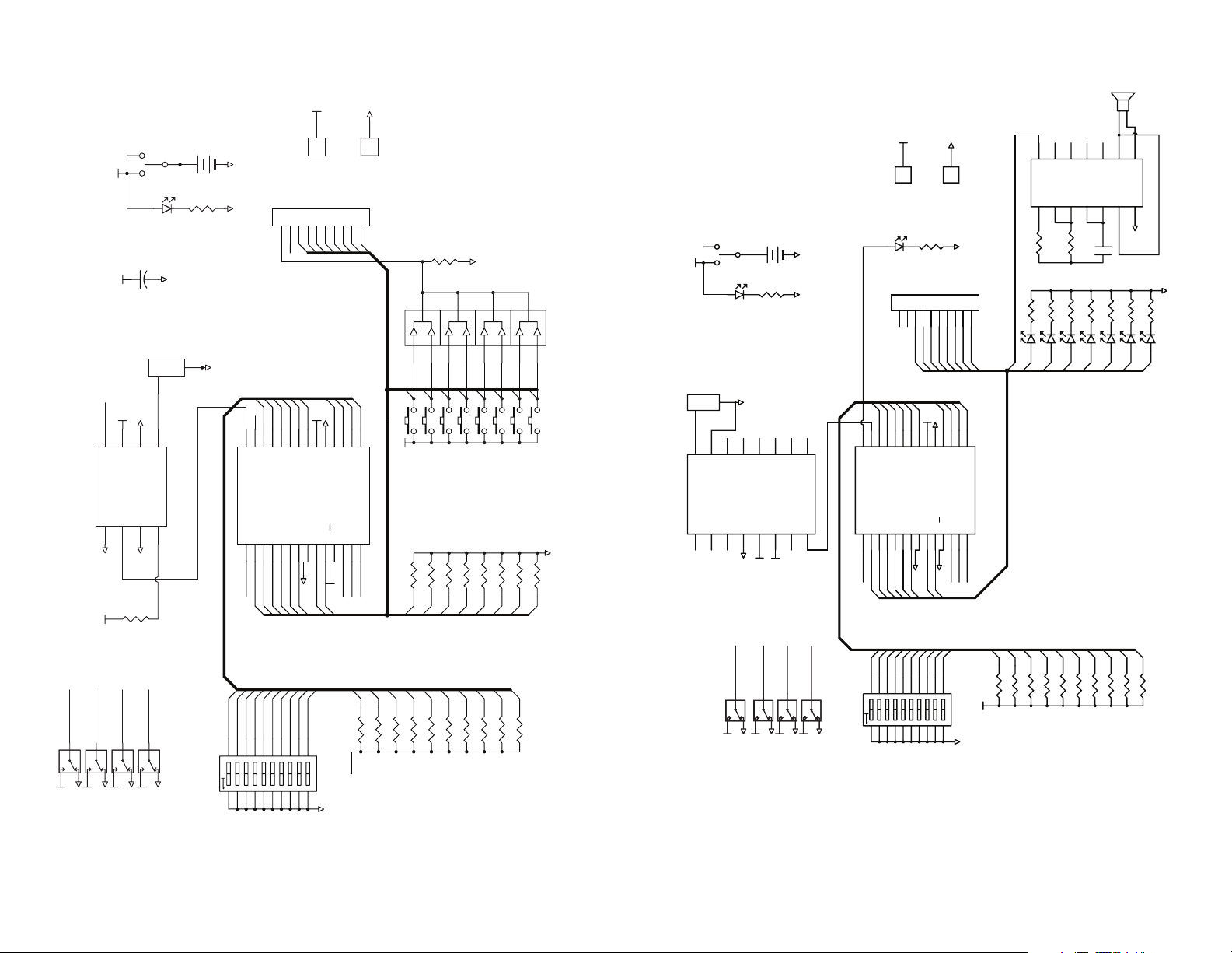
Figure 5: DS Series Encoder Board Schematic
P_SEL
D_CFG
A_CFG0
A_CFG1
SW2
SW3
GND
VCC
GND
SW4
VCC
GND
A9
171615
141312
456
789
10 11
– – – –
10 11
A1A2A3A4A5A6A7A8A9
R5 100K
R6 100K
R4 100K
R3 100K A0
TE
GND
R8 100K
R11 100K
R13 100K
R15 100K
R17 100K
R19 100K
Figure 6: DS Series Decoder Board Schematic
SW1
VCC
GND
VCC
A0A1A2A3A4A5A6A7A8
201918
171615
S1
123
456
141312
789
A9
10 11
A0A1A2A3A4A5A6A7A8
100k
100k
100k
100k
R4R5R8
R3
R2
VCC
GND
100k
100k
R10
100k
R13
100k
R14
100k
R16
A9
100k
R18
Page 9

Linx Technologies
159 Ort Lane
Merlin, OR, US 97532
Phone: +1 541 471 6256
Fax: +1 541 471 6251
www.linxtechnologies.com
Disclaimer
Linx Technologies is continually striving to improve the quality and function of its products. For this reason, we
reserve the right to make changes to our products without notice. The information contained in this Data Guide
is believed to be accurate as of the time of publication. Specifications are based on representative lot samples.
Values may vary from lot-to-lot and are not guaranteed. “Typical” parameters can and do vary over lots and
application. Linx Technologies makes no guarantee, warranty, or representation regarding the suitability of any
product for use in any specific application. It is the customer’s responsibility to verify the suitability of the part for
the intended application. NO LINX PRODUCT IS INTENDED FOR USE IN ANY APPLICATION WHERE THE SAFETY
OF LIFE OR PROPERTY IS AT RISK.
Linx Technologies DISCLAIMS ALL WARRANTIES OF MERCHANTABILITY AND FITNESS FOR A PARTICULAR
PURPOSE. IN NO EVENT SHALL LINX TECHNOLOGIES BE LIABLE FOR ANY OF CUSTOMER’S INCIDENTAL OR
CONSEQUENTIAL DAMAGES ARISING IN ANY WAY FROM ANY DEFECTIVE OR NON-CONFORMING PRODUCTS
OR FOR ANY OTHER BREACH OF CONTRACT BY LINX TECHNOLOGIES. The limitations on Linx Technologies’
liability are applicable to any and all claims or theories of recovery asserted by Customer, including, without
limitation, breach of contract, breach of warranty, strict liability, or negligence. Customer assumes all liability
(including, without limitation, liability for injury to person or property, economic loss, or business interruption) for
all claims, including claims from third parties, arising from the use of the Products. The Customer will indemnify,
defend, protect, and hold harmless Linx Technologies and its officers, employees, subsidiaries, affiliates,
distributors, and representatives from and against all claims, damages, actions, suits, proceedings, demands,
assessments, adjustments, costs, and expenses incurred by Linx Technologies as a result of or arising from any
Products sold by Linx Technologies to Customer. Under no conditions will Linx Technologies be responsible for
losses arising from the use or failure of the device in any application, other than the repair, replacement, or refund
limited to the original product purchase price. Devices described in this publication may contain proprietary,
patented, or copyrighted techniques, components, or materials. Under no circumstances shall any user be
conveyed any license or right to the use or ownership of such items.
©2015 Linx Technologies. All rights reserved.
The stylized Linx logo, Wireless Made Simple, WiSE, CipherLinx and the stylized CL logo are trademarks of Linx Technologies.
 Loading...