

Page 1

TRM-868-EUR
RF Transceiver Module
Data Guide
Page 2

Warning: Some customers may want Linx radio frequency (“RF”)
!
products to control machinery or devices remotely, including machinery
or devices that can cause death, bodily injuries, and/or property
damage if improperly or inadvertently triggered, particularly in industrial
settings or other applications implicating life-safety concerns (“Life and
Property Safety Situations”).
Table of Contents
1 Description
2 Ordering Information
2 Absolute Maximum Ratings
NO OEM LINX REMOTE CONTROL OR FUNCTION MODULE
SHOULD EVER BE USED IN LIFE AND PROPERTY SAFETY
SITUATIONS. No OEM Linx Remote Control or Function Module
should be modified for Life and Property Safety Situations. Such
modification cannot provide sufficient safety and will void the product’s
regulatory certification and warranty.
Customers may use our (non-Function) Modules, Antenna and
Connectors as part of other systems in Life Safety Situations, but
only with necessary and industry appropriate redundancies and
in compliance with applicable safety standards, including without
limitation, ANSI and NFPA standards. It is solely the responsibility
of any Linx customer who uses one or more of these products to
incorporate appropriate redundancies and safety standards for the Life
and Property Safety Situation application.
Do not use this or any Linx product to trigger an action directly
from the data line or RSSI lines without a protocol or encoder/
decoder to validate the data. Without validation, any signal from
another unrelated transmitter in the environment received by the module
could inadvertently trigger the action.
All RF products are susceptible to RF interference that can prevent
communication. RF products without frequency agility or hopping
implemented are more subject to interference. This module does not
have a frequency hopping protocol built in.
Do not use any Linx product over the limits in this data guide.
Excessive voltage or extended operation at the maximum voltage could
cause product failure. Exceeding the reflow temperature profile could
cause product failure which is not immediately evident.
Do not make any physical or electrical modifications to any Linx
product. This will void the warranty and regulatory and UL certifications
and may cause product failure which is not immediately evident.
3 Electrical Specications
5 Pin Assignments
5 Pin Descriptions
6 Theory of Operation
7 Module Description
8 Digital Transmission System (DTS)
9 Protocol
11 Reset to Factory Default
11 Hardware Reset
11 Voltage Supply Rise Time
11 The CMD Line
12 The UART Interface
12 Conguration Command Formatting
14 Conguration Registers
16 Writing to Registers
16 Reading from Registers
18 Conguration Registers
29 Typical Applications
30 Power Supply Requirements
30 Antenna Considerations
31 Helpful Application Notes from Linx
32 Interference Considerations
33 Pad Layout
33 Board Layout Guidelines
35 Microstrip Details
36 Production Guidelines
Page 3

36 Hand Assembly
36 Automated Assembly
38 General Antenna Rules
40 Common Antenna Styles
42 Regulatory Considerations
TRM-868-EUR
RF Transceiver Module
Data Guide
0.935
Description
The TRM-868-EUR combines a state-of-the art
low power wireless transceiver with a powerful
multipoint-to-multipoint protocol controller
to form a complete wireless communication
solution capable of replacing wires in almost any
RS-232/422/485 application. With a 115dB link
budget and very low power operation modes,
the DTS Series is excellent for AMR, RFID,
Home Automation, and any other application
requiring long range (1 mile / 1.6km line of sight) and long battery life.
Features
• True UART to antenna solution
• 16-bit CRC error checking
• 76.8kbps max RF data rate
• 2 channels in DTS mode
• 6 channels in LP mode
• Small size – 0.8" x 0.935" (20.32
x 23.75mm)
• Low power Standby and Sleep
modes
• CSMA medium access control
• 115dB link budget in DTS mode
• 4 modes allow user to optimize
power/range
• Command mode for volatile and
non-volatile configuration
• 48-bit unique address
• 5 volt tolerant I/O
• 915MHz U.S. version available
• Includes PHY and MAC protocol
0.800”
(20.32mm)
0.110”
(2.80mm)
Figure 1: Package Dimensions
(23.75mm)
A large-print version of this document is available at
www.linxtechnologies.com.
Applications
• Direct RS-232/422/485 Wire
replacement (requires external
RS-232 to 3V CMOS conversion
circuitry)
• Asset tracking
• Automated meter reading
• Industrial and/or home
automation
• RFID
• Wireless sensors
• Remote data logging
• Fleet management
– –
1
Revised 3/18/2015
Page 4
Electrical SpecicationsOrdering Information
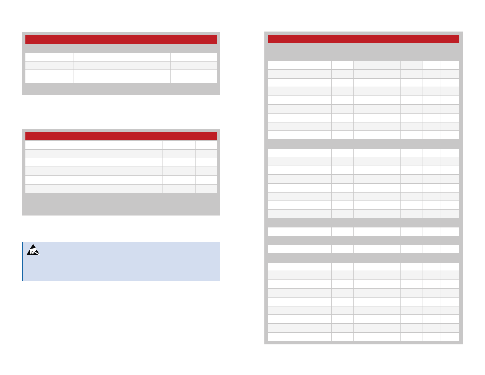
Ordering Information
Part Number Description Radiotronix Cross
TRM-868-EUR 868MHz EUR Series Transceiver WI.232EUR
TRM-915-DTS 900MHz DTS Series Transceiver Wi.232DTS-R
TRM-915-DTS-BRZ
900MHz DTS Series Transceiver - Brazil
Channels
Wi.232DTSB-R
Transceivers are supplied in trays of 50 pieces
Figure 2: Ordering Information
Absolute Maximum Ratings
Absolute Maximum Ratings
Supply Voltage V
cc
Any Input or Output Pin −0.3 to 5.0 VDC
Supply Voltage Rise Time 1 ms
RF Input 15 dBm
Operating Temperature −40 to +85 ºC
Storage Temperature −40 to +85 ºC
Exceeding any of the limits of this section may lead to permanent damage to the device.
Furthermore, extended operation at these maximum ratings may reduce the life of this
device.
Figure 3: Absolute Maximum Ratings
Warning: This product incorporates numerous static-sensitive
components. Always wear an ESD wrist strap and observe proper ESD
handling procedures when working with this device. Failure to observe
this precaution may result in module damage or failure.
−0.3 to +3.6 VDC
EUR Series Transceiver Specifications
Parameter Symbol Min. Typ. Max. Units Notes
Power Supply
Operating Voltage V
TX Supply Current l
CC
CCTX
2.7 3.0 3.6 VDC
1,2,5
Low Power 24–32 mA
Mid-Low Power 28–36 mA
Mid-High Power 35–43 mA
High Power 50–58 mA
RX Supply Current l
Standby Current l
Sleep Current l
CCRX
STD
PDN
16–24 mA 1,3
850 µA 1
35 100 µA 1
RF Section
Operating Frequency Band F
868.225 869.885 MHz
C
Center Frequency Accuracy 2 3 PPM
Number of Channels
DTS Mode 2
LP Mode 6
Channel Spacing
DTS Mode 650 kHz
LP Mode Variable kHz
Antenna Port
RF Impedance R
I N
50 Ω
Environmental
Operating Temp. Range −40 +85 ºC
Receiver Section
Receiver Sensitivity
DTS Mode @ 2.4kbps –106 dBm
DTS Mode @115.2kbps –102 dBm
LP Mode @2.4kbps –107 dBm
LP Mode @9.6kbps –104 dBm
Input IP3 −40 dBm 4
LO Leakage −65 dBm 5
Adjacent Channel Rejection –48 dBc 6
IF Bandwidth
– –
2 3
– –
Page 5
EUR Series Transceiver Specifications
Parameter Symbol Min. Typ. Max. Units Notes
DTS Mode 600 kHz
LP Mode 200 kHz
Transmitter Section
Output Power P
Harmonic Emissions P
O
H
13 15 dBm
-50 dBc 5
Frequency Deviation
DTS Mode ±80 kHz
LP Mode ±40 kHz
Interface Section
Input
Logic Low V
Logic High V
I L
I H
0 0.3*Vcc VDC
0.7*Vcc 5.0 VDC
Output
Logic Low V
Logic High V
OL
OH
0 0.4 VDC
2.5 Vcc VDC
Flash Specifications (Non-Volatile Registers)
Flash Write Duration 16 21 ms
Flash Write Cycles 20k 100k cycles
1. Vcc = 3.3VDC
2. Varies with data rate
3. Continuous operation, varies with
4. FLO+1MHz and FLO+1.945MHz
5. Into a 50-ohm load
6. Fc ± 650kHz
UART data rate
Figure 4: Electrical Specifications
Pin Assignments
21
3
NC
4
CMD
5
RXD
6
TXD
7
CTS
8
NC
9
NC
10
C2D
11
RESET
12
GND
13
ANT
14 15
GND
NC
GND
Figure 5: EUR Series Transceiver Pin Assignments (Top View)
Pin Descriptions
Pin Descriptions
Pin Number Name I/O Description
1, 12, 14, 15,
16, 17, 18
2, 3, 8, 9 NC —
4 CMD I
5 RXD I
6 TXD O
7 CTS O
10 C2D — Reserved
11 RESET — Reserved
13 ANT — 50-ohm RF Antenna Port
19 VCC — Supply Voltage
GND — Ground
No Electrical Connection. Do not connect
any traces to these lines.
Command Input. This line sets the serial
data as either command data to configure
the module or packet data to be sent over
the air. Pull low for command data; pull high
for packet data.
UART Receive Data Input. This is the input
line for the configuration commands as well
as data to be sent over the air.
UART Transmit Data Output. This is the
output line for the configuration command
responses as well as the data received over
the air.
UART Clear To Send, active low. This line
indicates to the host microcontroller when
the module is ready to accept data. When
CTS is high, the module is busy. When CTS
is low, the module is ready for data.
VCC
GND
GND
GND
GND
19
18
17
16
Figure 6: EUR Series Transceiver Pin Descriptions
– –
4 5
– –
Page 6
Theory of Operation
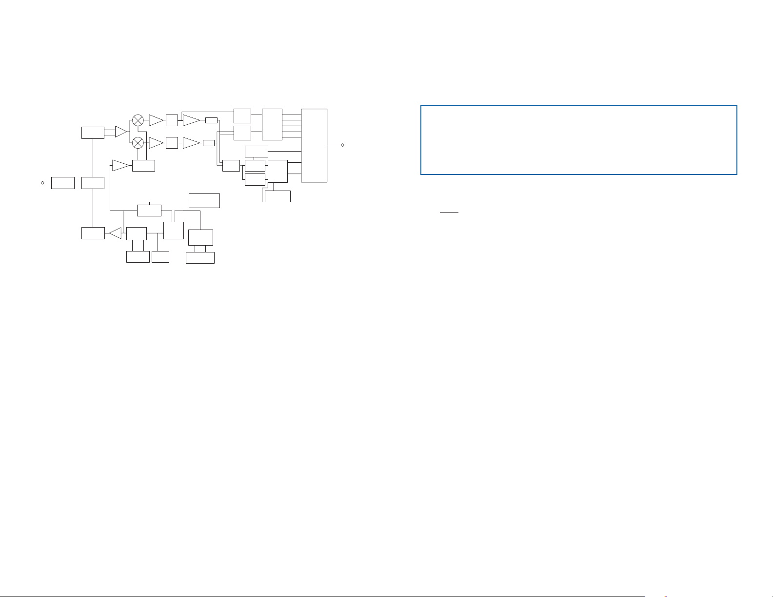
The EUR Series transceiver is a low-cost, high-performance synthesized
FSK transceiver. Its wideband operation gives it outstanding range while
still meeting regulatory requirements. Figure 7 shows a block diagram for
the module.
ANTENNA
SAW
FILTER
MATCHING
NETWORK
ANTENNA
SWITCH
MATCHING
NETWORK
LNA
LO_BUF
PA
VCO
TANK
VCO
PHASE
SHIFTER
MMOD
DIVIDER
FAMP
FAMP
LOOP
FILTER
LPF
LPF
CH PUMP
PFD
BBAMP LIM
LIM
BBAMP
∑∆ modulator
/n
Synthesizer
OSCILLATOR
39MHz
XTAL
DEMOD
RSSI
CONTROL
DATA
FEI
PATTERN
MATCHING
BITSYNC
11 Bits
BARKER
DECODER
LOGIC
CONTROL
11 Bits
BARKER
ENCODER
PROCESSOR
INTERFACE
UART /
Module Description
The EUR Series RF transceiver module has a Universal Asynchronous
Receiver Transmitter (UART) serial interface and is designed to create
a complete UART-to-antenna wireless solution capable of direct wire
replacement in most embedded RS-232/422/485 applications.
Note: Although the module is capable of supporting the serial data
communications required by RS-232, RS-422, and RS-485 networks,
it is not compatible with the electrical interfaces for these types of
networks. The module has CMOS inputs and outputs and requires an
appropriate converter for the particular type of network being used.
The module is designed to interface directly to a host UART. Three lines are
used to transfer data between the module and the host UART: TXD, RXD
and CTS. TXD is the data output from the module. RXD is the data input
to the module. The CTS output indicates if the module is ready to accept
data. The UART interface is capable of operating in full duplex at baud
rates from 2.4 to 115.2kbps.
Figure 7: EUR Series Transceiver Block Diagram
The EUR Series transceiver is designed for operation in the 868 to 870MHz
frequency band. The RF synthesizer contains a VCO and a low-noise
fractional-N PLL. The receive and transmit synthesizers are integrated,
enabling them to be automatically configured to achieve optimum phase
noise, modulation quality and settling time.
The transmitter output power is programmable from −2dBm to +15dBm.
The frequency deviation is optimized to deliver the highest performance
over a wide range of data rates.
The receiver incorporates highly efficient low-noise amplifiers that provide
up to –102dBm sensitivity.
An onboard controller performs the radio control and management
functions. A processor performs the higher level protocol functions and
controls the serial and hardware interfaces.
The module has a built-in protocol that automatically transmits the data
input on the UART. All encoding, transmitting, receiving and decoding
functions are handled by the internal processor, so no overhead is required
by an external processor.
The module can be put into a Sleep mode through serial commands. In
Sleep mode, the RF section is completely shut down and the protocol
processor is in an idle state. Once the module has been placed in the sleep
mode, it can be awakened by sending a power-up sequence through the
serial port.
If the current draw in sleep mode is too high for a particular application,
the designer can switch power to the module through a FET to turn off the
module when it is not needed. If this technique is used, the volatile registers
reset to the values in their non-volatile mirrors, so any changes from the
default will have to be reloaded.
Every module has a 48-bit MAC address that can be used by the host
application to uniquely identify each module. This MAC address can be
read through the command interface.
– –
6 7
– –
Page 7

Digital Transmission System (DTS)
The EUR Series transceiver utilizes a DTS digital spread spectrum
technique. This technique increases the transmission bandwidth to over
500KHz and the outgoing RF data is encoded with symbols selected to
ensure its average duty cycle is 50%.
In DTS mode, the module’s channel bandwidth is set to 600kHz and the
transmit power is set to one of four selectable levels. In this mode, the
module can operate on 2 channels and support a maximum RF data rate
of 76.8kbps. The receiver sensitivity at the max data rate is –102dBm
typical, yielding a link budget of 115dB. This mode is an excellent
alternative to Frequency Hopping Spread Spectrum (FHSS). It has no
synchronization requirements, allowing it to operate in a duty-cycle mode
for extended battery life.
In low-power (LP) mode, the module’s channel bandwidth is set to 200kHz
and the transmit power is set to one of four selectable levels. In this mode,
the module can operate on 6 channels and support a maximum data rate
of 9.6kbps. The receiver sensitivity at the maximum data rate is –104dBm
typical, yielding a link budget of 117dB. This mode reduces transmit
current consumption, allowing use with batteries that cannot supply the
pulse currents required for DTS mode.
DTS Systems have several advantages over FHSS and Direct Sequence
Spread Spectrum (DSSS) systems. A DTS system operates on one RF
channel at a time, so there is no interruption of the data transfer. FHSS
systems have to stop sending data when they hop to a new channel. FHSS
systems also have to synchronize the transmitter and receiver to make sure
that they hop to the same channel at the same time. This synchronization
can take 25ms or more while a DTS system can wake up in less than
10ms. Further, FCC regulations require that FHSS systems use each
channel equally, so they frequently send null data just to use a channel.
This increases current consumption, which is a disadvantage in battery
operated devices.
DSSS systems also operate on one channel at a time, but their hardware
implementations are much more expensive that a DTS system. Their
channels are much wider which means that a DSSS receiver’s sensitivity is
much lower than a DTS system.
Both FHSS and DSSS systems can operate at higher power levels than
DTS systems, depending on the energy density of the DTS system.
However, a DTS system is a good compromise between FHSS and DSSS.
Protocol
The built-in protocol has a number of features that make it a robust system.
When the module has a packet to send, it uses a Carrier-Sense-MultipleAccess (CSMA) protocol to determine if another module is already
transmitting. If so, the module receives that data before attempting to
transmit its data again. If the UART receive buffer gets full, the CTS line
goes high to prevent the host UART from over-running the receive buffer.
The CSMA mechanism introduces a variable delay to the transmission
channel. This delay is the sum of a random period and a weighted period
that is dependent on the number of times that the module has tried and
failed to access the channel. For applications that guarantee that only one
module is transmitting at any given time, the CSMA mechanism can be
turned off to avoid this delay.
The module prefixes the data with a packet header and postfixes the data
with a 16-bit CRC. The 16-bit CRC error checking can be disabled to allow
the host application to do its own error checking. Data is encoded using
a proprietary algorithm to spread the RF energy within the transmission
bandwidth and meet regulatory requirements.
Each module can be assigned a 7-bit group ID, which is used to logically
link it to other modules on the same channel. Any data received from a
module with a different group ID is discarded.
Modules can also operate in two network modes: Master/Slave and
Peer-to-Peer. These modes define a set of communication rules that
identifies which modules can talk to any given module. In Master/Slave
mode, masters can talk to slaves and other masters, slaves can talk to
masters, but slaves cannot talk to other slaves. This mode is sometimes
required for applications that are replacing legacy RS-485 networks. In
peer-to-peer mode, any module can talk to any other module. In both
modes, group integrity is enforced.
When a module transmits a packet, all other modules on the same channel
receive the packet, check the packet for errors, determine whether the
received group ID matches the local group ID, and compare the sender’s
master/slave flag to its internal setting. If the packet is error free, the group
– –
8 9
– –
Page 8
0xFF ...B1B0
IDs match, and the master/slave rules are satisfied (if peer to peer is
RF ISR
UART RX
selected in the receiving module, this test passes regardless), the module
decodes the data and outputs it on the RXD line.
The primary state when the module is not actively transmitting or receiving
data is the IDLE state. While in this state, the receiver is enabled and the
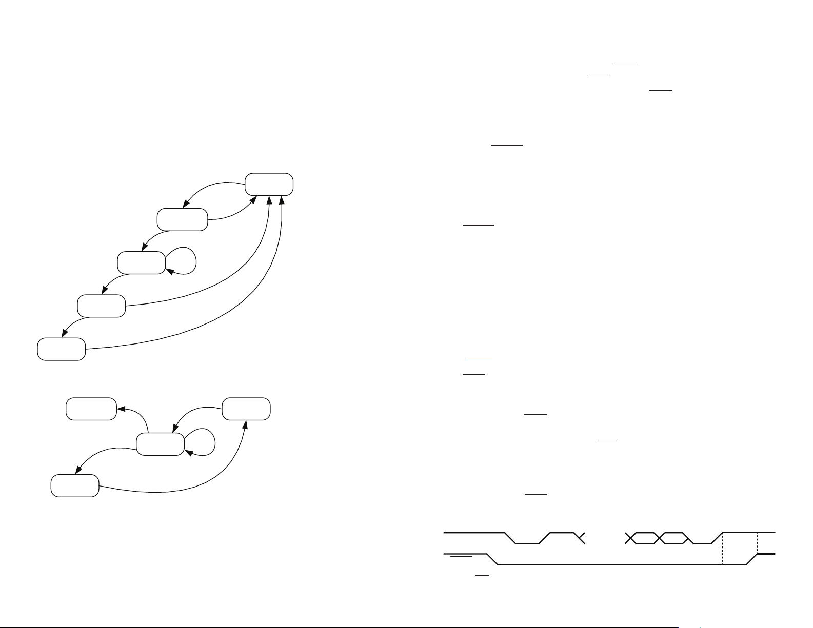
module is continuously listening for incoming data. If the module detects
a pre-amble and valid start-code, it enters the RX HEADER state. Figure 8
shows the receiver state diagram and Figure 9 shows the transmitter state
diagram.
IDLE MODE
RX HEADER
HEADER OK
DATA LENGTH < MTU
RX DATA
RX DONE
CRC FAILED
CRC
RF ISR
PACKET
QUEUED
UART TX
RX TIMEOUT
Reset to Factory Default
It may be necessary to reset the non-volatile registers to their factory
defaults. To reset the module, hold the CMD line low and cycle power to
hardware-reset the module. The CMD line must remain low for a minimum
of 600ms after resetting the module. Once the CMD line is released, the
module’s non-volatile registers are reset to factory defaults.
Hardware Reset
Pulling the RESET line low places the module’s protocol controller in
hardware reset. In this state, the module is in a safe, stalled state. If the
voltage supply rise time is greater than 1ms, the module should be held in
reset until Vcc reaches 2.7V. There are many reset supervisor ICs that can
accomplish this task.
The RESET line must be held low for at least 20µs to cause the module to
enter reset. Normal operation is restored when this pin is returned high.
Voltage Supply Rise Time
The power supply rise time is extremely important. It must rise from ground
to 2.7V in less than 1ms. If this specification cannot be met, an external
reset supervisor circuit must be used to hold the module in reset until the
power supply stabilizes. Failure to ensure adequate power supply rise time
can result in loss of important module configuration information.
Figure 8: EUR Series Transceiver Receiver State Diagram
RX HEADER
DATA LENGTH ≥ MTU
OR TX TIMEOUT
CSMA
Figure 9: EUR Series Transceiver Receiver State Diagram
RF ISR
TX WAIT
DATA LENGTH < MTU
TX COMPLETE
The CMD Line
The CMD line is used to inform the module where incoming UART data
should be routed. When the line is high or left floating, all incoming UART
IDLE MODE
– –
10 11
data is treated as payload data and is routed to the transmitter to be sent
over the air. If the CMD line is low, the incoming UART data is routed to
the command parser for processing. Since the module’s processor looks at
UART data one byte at a time, the CMD line must be held low for the entire
duration of the command plus a 20µs margin for processing. Leaving the
line low for additional time (for example, until the ACK byte is received by
your application) does not adversely affect the module. If RF packets are
received while the CMD line is active, they are still processed and output on
the module’s UART. Figure 10 shows this timing.
RXD
CMD
Figure 10: CMD Line Timing
≥20µs
– –
Page 9

The UART Interface
The module uses a standard UART interface for both data to be sent over
the air and for configuring the module. The CMD line is used to tell the
module if the data on the UART is for configuration or transmission. The
lines follow the standard UART naming convention, so RXD is the data
input into the module and TXD is the data output from the module.
The module has a 192 byte buffer for incoming data. The module can be
programmed to automatically transmit when the buffer reaches a limit or
based on the time between bytes on the UART. This allows the designer to
optimize the module for fixed length and variable length data. The module
supports streaming data as well. To optimize the module for streaming
data, regUARTMTU should be set to 144, and regTXTO should be set to a
value greater than 1 byte time at the current UART data rate.
If the buffer gets full or the timer set by regTXTO expires while the module
is still in the process of sending the previous packet over the RF link, the
module sets the CTS line high, indicating that the host should not send any
more data. Data sent by the host while CTS is high is lost.
Conguration Command Formatting
The EUR Series module contains several volatile and non-volatile registers
that control its configuration and operation. The volatile registers all
have non-volatile mirror registers that are used to determine the default
configuration when power is applied to the module. During normal
operation, the volatile registers are used to control the module.
Placing the module in the command mode allows these registers to be
programmed. Byte values in excess of 127 (0x80 or greater) must be
changed into a two-byte escape sequence of the format:
0xFE, [value - 128]
For example, the value 0x83 becomes 0xFE, 0x03. The function in Figure
11 prepends a 0xFF header and size specifier to a command sequence
and creates escape sequences as needed. It is assumed that *src is
populated with either the register number to read (one byte, pass 1 into
src_len) or the register number and value to write (two bytes, pass 2 into
src_len). It is also assumed that the *dest buffer has enough space for the
two header characters plus the encoded command and the null terminator.
int EscapeString(char *src, char src_len, char *dest)
{
// The following function copies and encodes the rst
// src_len characters from *src into *dest. This
// encoding is necessary for module command formats.
// The resulting string is null terminated. The size
// of this string is the function return value.
// ---------------------------------------------------
char src_idx, dest_idx;
// Save space for the command header and size bytes
// ------------------------------------------------
dest_idx = 2;
// Loop through source string and copy/encode
// ------------------------------------------
for (src_idx = 0; src_idx < src_len; src_idx++)
{
if (src[src_idx] > 127)
{
dest[dest_idx++] = 0xFE;
}/*if*/
dest[dest_idx++] = (src[src_idx] & 0x7F);
}/*for*/
// Add null terminator
// -------------------
dest[dest_idx] = 0;
// Add command header
// ------------------
dest[0] = 0xFF;
dest[1] = dest_idx – 2;
// Return escape string size
// -------------------------
return dest_idx;
}
Figure 11: Command Conversion Code
– –
12 13
– –
Page 10
Conguration Registers
The EUR Series module contains several registers that control its
configuration and operation. The register settings are stored in two types
of memory inside the module. Volatile memory is quick to access, but it is
lost when power is removed from the module. Non-volatile memory takes
longer to access, but is retained when power is removed.
All of the configuration settings have registers in both types of memory.
The settings are read from non-volatile registers on power up and saved
in volatile registers since it is faster to read and write the volatile memory
locations. There are commands to read and write both locations.
During normal operation, the volatile registers are used to control the
module. Figure 13 shows all of the configuration registers. Figure 12 shows
the default values for the non-volatile registers. These are what the module
uses when it powers up. Changing these values changes the module’s
default setting.
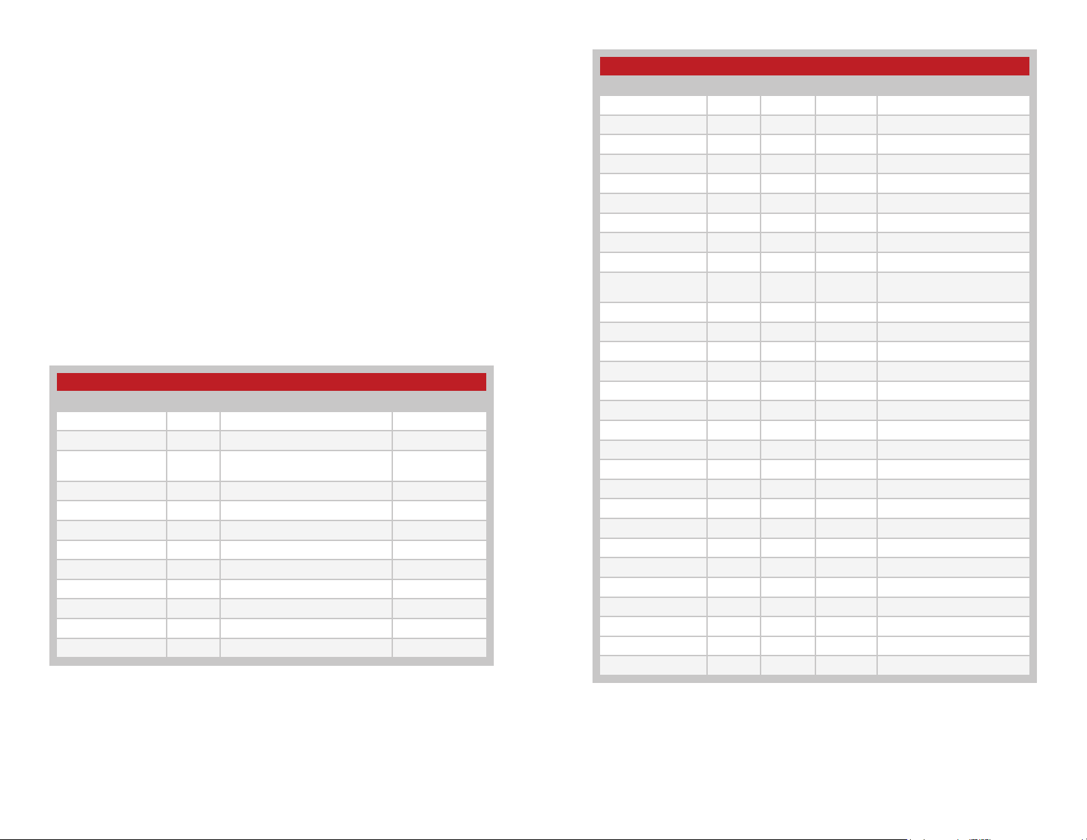
Non-Volatile Register Default Values
Name Address Description Default Value
regNVTXCHANNEL 0x00 Transmit channel setting 0
regNVRXCHANNEL 0x01 Receive channel setting 0
regNVPWRMODE 0x02 Operating mode settings
regNVDATARATE 0x03 UART data rate 2400bps
regNVNETMODE 0x04 Network mode (Normal/Slave) Normal
regNVTXTO 0x05 Transmit wait timeout ~16ms
regNVNETGRP 0x06 Network group ID 0x00
regNVUSECRC 0x08 Enable/disable CRC Enabled
regNVUARTMTU 0x09 Minimum transmission unit 64 bytes
regNVSHOWVER 0x0A Enable/disable start-up message Enabled
regNVCSMAMODE 0x0B Enable/disable CSMA Enabled
regNVSLPMODE 0x0D Power state of module Awake
Figure 12: EUR Series Non-volatile Configuration Register Default Settings
+13dBm
DTS mode
EUR Series Configuration Registers
Name Address Location Operation Description
regNVTXCHANNEL 0x00 NV R/W Transmit channel setting
regNVRXCHANNEL 0x01 NV R/W Receive channel setting
regNVPWRMODE 0x02 NV R/W Operating mode settings
regNVDATARATE 0x03 NV R/W UART data rate
regNVNETMODE 0x04 NV R/W Network mode (Normal/Slave)
regNVTXTO 0x05 NV R/W Transmit wait timeout
regNVNETGRP 0x06 NV R/W Network group ID
regNVUSECRC 0x08 NV R/W Enable/disable CRC
regNVUARTMTU 0x09 NV R/W Minimum transmission unit
regNVSHOWVER 0x0A NV R/W
regNVCSMAMODE 0x0B NV R/W Enable/disable CSMA
regNVSLPMODE 0x0D NV R/W Power state of module
regMAC5 0x22 NV R MAC address byte 5
regMAC4 0x23 NV R MAC address byte 4
regMAC3 0x24 NV R MAC address byte 3
regMAC2 0x25 NV R MAC address byte 2
regMAC1 0x26 NV R MAC address byte 1
regMAC0 0x27 NV R MAC address byte 0
regTXCHANNEL 0x4B V R/W Transmit channel setting
regRXCHANNEL 0x4C V R/W Receive channel setting
regPWRMODE 0x4D V R/W Operating mode settings
regDATARATE 0x4E V R/W UART data rate
regNETMODE 0x4F V R/W Network mode (normal/slave)
regTXTO 0x50 V R/W Transmit wait timeout
regNETGRP 0x51 V R/W Network group ID
regUSECRC 0x53 V R/W Enable/disable CRC
regUARTMTU 0x54 V R/W Minimum transmission unit
regCSMAMODE 0x56 V R/W Enable/disable CSMA
regSLPMODE 0x58 V R/W Power state of module
Figure 13: EUR Series Configuration Registers
Enable/disable start-up
message
– –
14 15
– –
Page 11

Writing to Registers
Writing to a volatile register is nearly instantaneous. Writing to a non-volatile
register typically takes 16ms. Because the packet size can vary based on
the need for encoding, there are two possible packet structures. The first
structure writes a value that is less than 128 (ox80) and the second writes
a value that is higher. The higher value must be split into two values. The
following tables show the byte sequences for writing a register in each
case. Figure 14 shows the command to write to a register.
Channel Settings - Address = 0x4B, 0x4C; NV Address = 0x00, 0x01
The DTS Series supports 2 channels (0 – 1) in DTS mode and 6 channels
(0 – 5) in low power mode.
Transmit and receive channels are set in regTXCHAN (addr 0x4B) and
regRXCHAN (addr 0x4C) respectively. The non-volatile defaults are set in
regNVTXCHAN (addr 0x00) and regNVRXCHAN (addr 0x01) respectively.
The channel frequencies and their decimal values are shown in Figure 16.
Write to Configuration Register Command
Command for a Value less than 128 (0x80)
Header Size Address Value
0xFF 0x02 REG V1
Command for a Value greater than 128 (0x80)
Header Size Address Value 1 Value 2
0xFF 0x03 REG 0xFE V2
Figure 14: Write to Configuration Register Command
Warning: Be sure that the module is properly powered and remains
powered for the duration of the register write. Loss of important
configuration information could occur if the unit loses power during a
non-volatile write cycle.
Reading from Registers
A register read command is constructed by placing an escape character
(0xFE) before the register number. The module responds to this command
by sending an ACK (0x06) followed by the register number and register
value. The register value is sent unmodified. For example, if the register
value is 0x83, 0x83 is returned. If the register number is invalid, the module
responds with a NACK (0x15). The command and response are shown in
Figure 15.
Read From Configuration Register
Command
Header Size Escape Address
0xFF 0x02 0xFE REG
Response
ACK Address Value
0x06 REG V1
Note: If the module is set to different transmit and receive channels then
the CSMA algorithm will not work.
All modules in a network must be in the same mode (LP or DTS) and must
have the same transmit and receive channels programmed in order to
communicate properly.
Channel Settings
Read Command Read Response
Header Size Escape Address ACK Address Value
0xFF 0x02 0xFE ADDR 0x06 ADDR CHAN
Write Command
Header Size Address Value
0xFF 0x02 ADDR CHAN
Figure 17: Channel Settings Command and Response
DTS Series RF Channels
Channel LP Mode DTS Mode
0 868.225 868.300
1 868.375 868.950
2 868.850 N/A
3 869.050 N/A
4 869.525 N/A
5 869.850 N/A
Figure 16: EUR Series RF Channel Numbers and Frequencies
Figure 15: Read from Configuration Register Command and Response
– –
16 17
– –
Page 12

Conguration Registers
Power Mode - Address = 0x4D; NV Address = 0x02
The Power Mode register (regPWRMODE, addr 0x4D) configures the
operation mode (DTS or LP) and the transmitter output power setting. The
non-volatile register (regNVPWRMODE, addr 0x02) determines the default
setting on power up.
It is important to note that a module configured to operate in LP mode
does not work with a module transmitting in DTS mode, or vice versa.
However, a module configured to operate in any of the four DTS modes
does work with any other module transmitting in any of the DTS modes.
Power Mode
Read Command Read Response
Header Size Escape Address ACK Address Value
0xFF 0x02 0xFE
Write Command
Header Size Address Value
0xFF 0x02
Figure 18: Power Mode Command and Response
0x4D
0x02
0x4D
0x02
V1
0x06
0x4D
0x02
V1
UART Data Rate - Address = 0x4E; NV Address = 0x03
The UART data rate is set by the regDATARATE (addr 0x4E) register. The
default UART data rate is 2.4kbps but can be changed by setting the
regNVDATARATE (addr 0x03) register.
This rate must match the rate used by the processor that is connected to
the module. If the rates are not set to match, then either each rate can be
tried in turn or the module can be reset to factory defaults.
The rate should be limited to 9.6kbps in LP mode. Exceeding this rate
results in poor link quality.
Figure 20 shows example commands setting the UART data rate and
Figure 21 shows the available UART rate settings.
UART Data Rate
Read Command Read Response
Header Size Escape Address ACK Address Value
0xFF 0x02 0xFE
Write Command
Header Size Address Value
0xFF 0x02
0x4E
0x03
0x4E
0x03
V1
0x06
0x4E
0x03
V1
Power Mode Register Values
V1 Mode Power Setting Output Power
0x00 LP Mode Low -2dBm
0x01 DTS Mode Mid-low +2dBm
0x02 DTS Mode Mid-high +7dBm
0x03 DTS Mode High +13dBm
0x04 DTS Mode Low -2dBm
0x05 LP Mode Mid-low +2dBm
0x06 LP Mode Mid-high +7dBm
0x07 LP Mode High +13dBm
Figure 19: Power Mode Register Values
– –
18 19
Figure 20: UART Data Rate Command and Response
UART Data Rate Register Settings
V1 Baud Rate
0x00 2,400
0x01 9,600
0x02 19,200
0x03 38,400
0x04 57,600
0x05 115,200
0x06 10,400*
0x07 31,250*
* These data rates are not supported by PC serial ports.
Selection of these rates may cause the module to fail to
respond to a PC, requiring a reset to factory defaults.
Figure 21: UART Data Rate Register Settings
– –
Page 13
Network Mode - Address = 0x4F; NV Address = 0x04
The module supports two networking modes: Normal and Slave. In
normal mode, the module can talk to any other module. In slave mode,
the module can talk to normal-mode modules, but cannot transmit to or
receive from other slaves. Slave mode is selected by writing 0x00 to this
register. The default network mode is 0x01 (Normal Mode).
Transmit Wait Timeout - Address = 0x50; NV Address = 0x05
When a byte is received from the UART, the module starts a timer that
counts down every millisecond. The timer is restarted when each byte is
received. The value for this setting is the number of milliseconds to wait
before transmitting the data in the UART receive buffer. The default setting
for this register is 0x10 (~16ms delay).
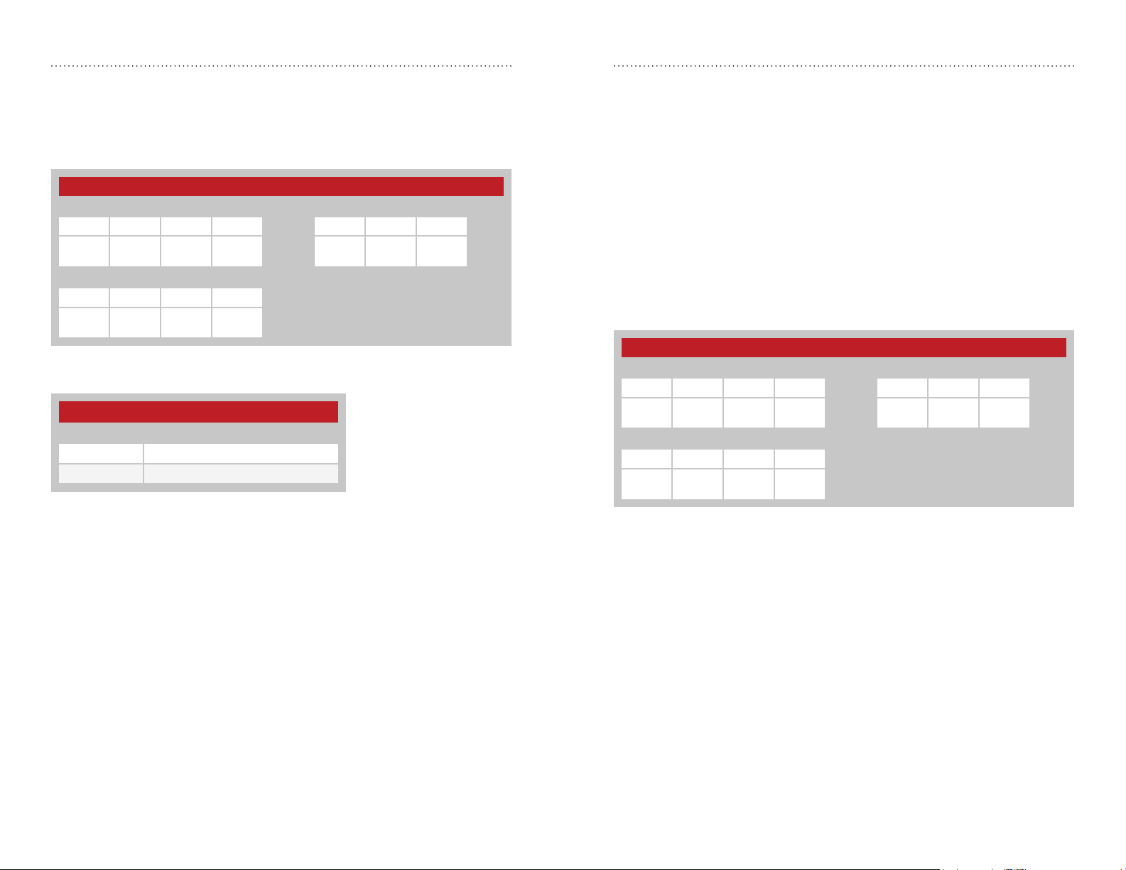
Network Mode
Read Command Read Response
Header Size Escape Address ACK Address Value
0xFF 0x02 0xFE
Write Command
Header Size Address Value
0xFF 0x02
Figure 22: Network Mode Command and Response
Network Mode Register Settings
V1 Mode
0x00 Slave Mode
0x01 Normal Mode
Figure 23: Network Mode Register Settings
0x4F
0x04
0x4F
0x04
V1
0x06
0x4F
0x04
V1
If the timer reaches zero before the next byte is received from the UART,
the module begins transmitting the data in the buffer. This timeout value
should be greater than one byte time at the current UART data rate.
If the timeout value is set to 0x00, the transmit wait timeout is deactivated.
In this case, the transceiver waits until a number of bytes equal to the MTU
have been received by the UART. All of the bytes are sent once the MTU
has been reached. Figure 24 shows examples of the commands.
Transmit Wait Timeout
Read Command Read Response
Header Size Escape Address ACK Address Value
0xFF 0x02 0xFE
Write Command
Header Size Address Value
0xFF 0x02
Figure 24: Transmit Wait Timeout Command and Response
0x50
0x05
0x50
0x05
V1
0x06
0x50
0x05
V1
– –
20 21
– –
Page 14
Network Group - Address = 0x51; NV Address = 0x06
Modules can be grouped into networks. Although only modules with the
same network group ID can communicate, modules in different network
groups but on the same RF channel still coordinate transmissions through
the CSMA mechanism. Valid values for this register are decimal 0 to
127. The default group setting is 0. Figure 25 shows examples of the
commands.
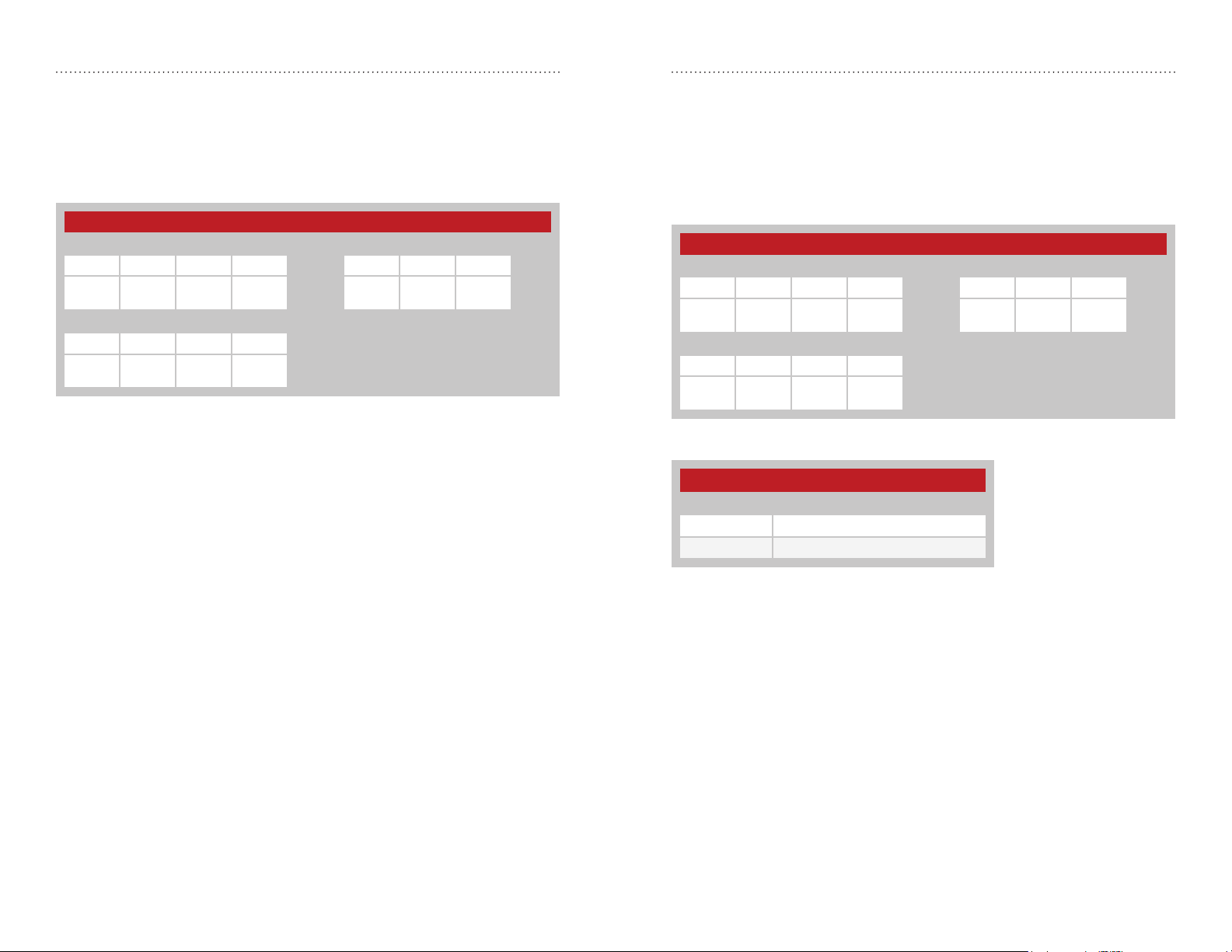
Network Group
Read Command Read Response
Header Size Escape Address ACK Address Value
0xFF 0x02 0xFE
Write Command
Header Size Address Value
0xFF 0x02
Figure 25: Network Group Command and Response
0x51
0x06
0x51
0x06
V1
0x06
0x51
0x06
V1
CRC Control - Address = 0x53; NV Address = 0x08
The EUR Series protocol includes a Cyclic Redundancy Check on the
received packets to make sure that there are no errors. Any packets with
errors are discarded and not output on the UART. This feature can be
disabled if it is desired to perform error checking outside the module. Set
the register to 0x01 to enable CRC checking, or 0x00 to disable it. The
default CRC mode setting is enabled. Figure 26 shows examples of the
commands and Figure 27 shows the available values.
CRC Control
Read Command Read Response
Header Size Escape Address ACK Address Value
0xFF 0x02 0xFE
Write Command
Header Size Address Value
0xFF 0x02
Figure 26: CRC Control Command and Response
CRC Control Register Settings
V1 Mode
0x00 CRC Disabled
0x01 CRC Enabled
0x53
0x08
0x53
0x08
V1
0x06
0x53
0x08
V1
Figure 27: CRC Control Register Settings
– –
22 23
– –
Page 15
UART Minimum Transmission Unit - Addr = 0x54; NV Addr = 0x09
This register determines the UART buffer level that triggers the transmission
of a packet. The minimum value is decimal 1 and the maximum value is
144. The default value for this register is 64, which provides a good mix of
throughput and latency. Figure 28 shows examples of the commands.
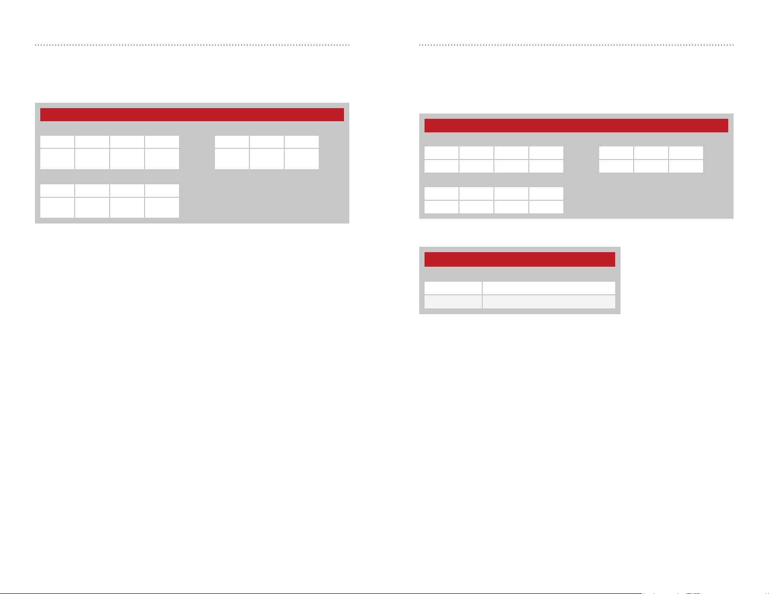
UART MTU
Read Command Read Response
Header Size Escape Address ACK Address Value
0xFF 0x02 0xFE
Write Command
Header Size Address Value
0xFF 0x02
0x54
0x09
0x54
0x09
V1
0x06
0x54
0x09
V1
Verbose Mode - NV Address = 0x0A
Setting this register to 0x00 suppresses the start-up message, including
firmware version, which is sent to the UART when the module is reset. A
value of 0x01 causes the message to be output after reset. By default,
the module start-up message is output. Figure 29 shows examples of the
commands and Figure 30 shows the available values.
Verbose Mode
Read Command Read Response
Header Size Escape Address ACK Address Value
0xFF 0x02 0xFE 0x0A 0x06 0x0A V1
Write Command
Header Size Address Value
0xFF 0x02 0x0A V1
Figure 28: UART MTU Command and Response
Figure 29: Verbose Mode Command and Response
Verbose Mode Register Settings
V1 Mode
0x00 Disable the start-up message
0x01 Enable the start-up message
Figure 30: Verbose Mode Register Settings
– –
24 25
– –
Page 16
CSMA Enable - Address = 0x56; NV Address = 0x0B
Carrier-Sense Multiple Access (CSMA) is a best-effort delivery system that
listens to the channel before transmitting a message. If another module is
already transmitting when a message is queued, the module waits before
sending its payload. This helps to eliminate RF message corruption at the
expense of additional latency. Setting this register to 0x01 enables CSMA
and 0x00 disables CSMA. By default, CSMA is enabled. Figure 31 shows
examples of the commands and Figure 32 shows the available values.
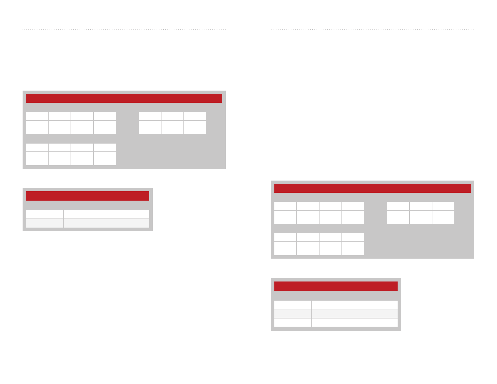
CSMA Enable
Read Command Read Response
Header Size Escape Address ACK Address Value
0xFF 0x02 0xFE
Write Command
Header Size Address Value
0xFF 0x02
Figure 31: CSMA Enable Command and Response
CSMA Enable Register Settings
V1 Mode
0x00 Disable CSMA
0x01 Enable CSMA
Figure 32: CSMA Enable Register Settings
0x54
0x09
0x54
0x09
V1
0x06
0x54
0x09
V1
Sleep Control - Address = 0x58; NV Address = 0x0D
Setting this register to 0x01 places the module into Sleep mode and 0x02
places the module in Standby mode. Sleep mode places the module in
the lowest power inactive state (~35µA) and requires approximately 7-8ms
to resume operation once awakened. The RF section is completely shut
down, and the protocol processor is in an idle, low-speed state. Any RF
data sent to the module while it is in Sleep mode is lost.
In Standby mode, the RF section is powered down except for the oscillator,
and the protocol processor is in an idle, low-speed state. Standby mode
draws ~850µA and requires approximately 1-2ms to awaken. Any RF data
sent to the module while it is in Standby mode is lost.
A sequence of four 0xFF bytes on the RXD line wakes the module up.
Upon awakening, the module clears the volatile register to 0x00. The
default value for this register is 0x00 (awake).
Figure 33 shows examples of the commands and Figure 34 shows the
available values.
Sleep Control
Read Command Read Response
Header Size Escape Address ACK Address Value
0xFF 0x02 0xFE
Write Command
Header Size Address Value
0xFF 0x02
0x58
0x0D
0x58
0x0D
V1
0x06
0x58
0x0D
V1
Figure 33: Sleep Control Command and Response
Sleep Control Register Settings
V1 Mode
0x00 Awake
0x01 Sleep Mode
0x02 Standby Mode
Figure 34: Sleep Control Register Settings
– –
26 27
– –
Page 17
ANTENNA
MAC Address - NV Address = 0x22, 0x23, 0x24, 0x25, 0x26, 0x27
The MAC Address registers make a 48-bit MAC address that uniquely
identifies each module. These values are factory preset and cannot be
altered. These bytes are not used by the module but are provided for use
as a unique address in the end applications. Figure 35 shows examples of
the command.
MAC Address
Read Command Read Response
Header Size Escape Address ACK Address Value
0xFF 0x02 0xFE ADDR 0x06 ADDR V1
Figure 35: MAC Address Command and Response
Typical Applications
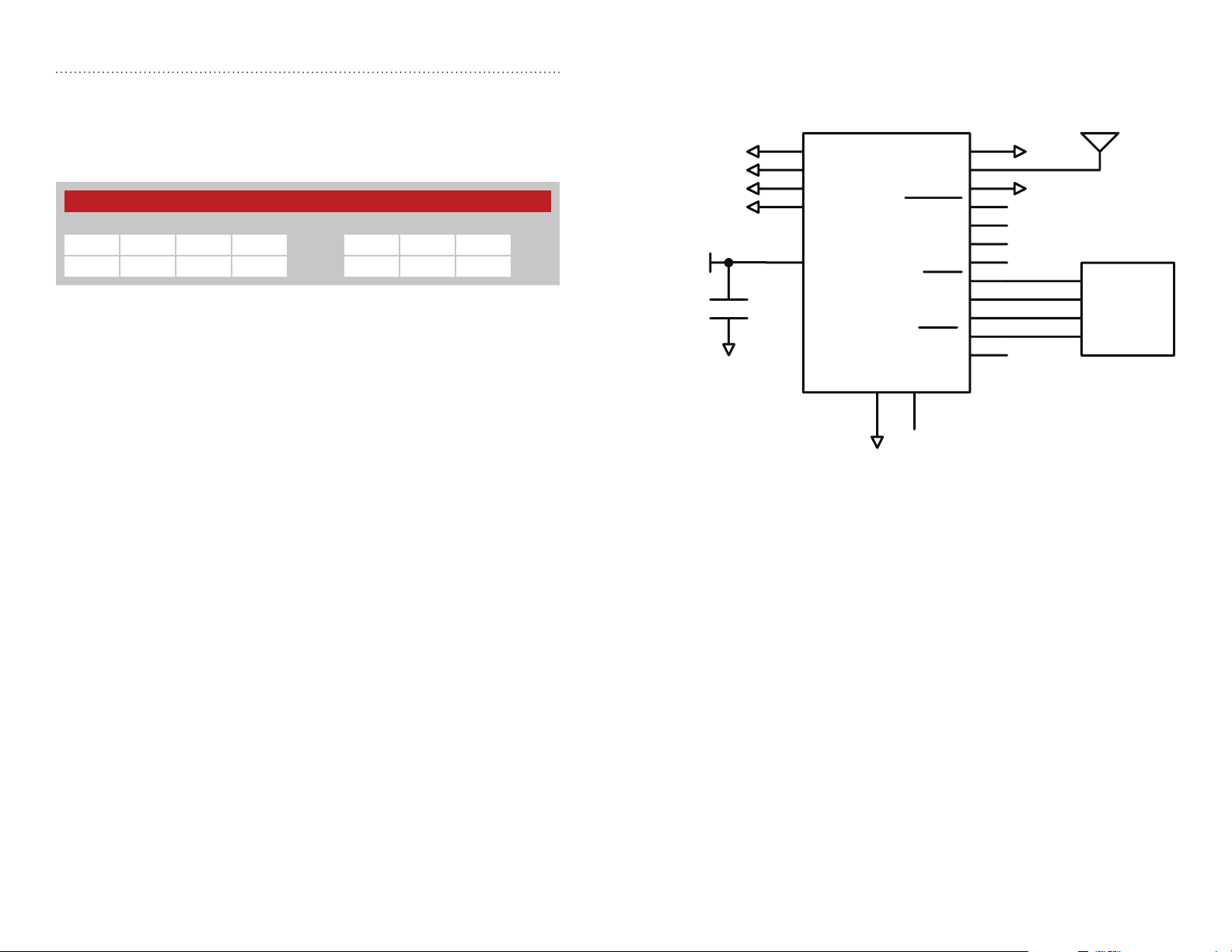
Figure 36 shows a circuit using the EUR Series transceiver.
GND
GND
GND
GND
VCC
GND
15
16
17
18
19
GND
GND
GND
GND
VCC
RESET
GND1NC
2
GND
Figure 36: EUR Series Transceiver Basic Application Circuit
GND
ANT
GND
C2D
NC
NC
CTS
TXD
RXD
CMD
NC
14
13
12
11
10
9
8
7
6
5
4
3
GND
GND
GPIO
RXD
TXD
GPIO
µ
The transceiver UART is connected to a microcontroller UART for
communication of configuration data and data to be sent over the air.
There is no need for buffering or other circuitry between the transceiver and
microcontroller provided that both are operating on the same voltage.
– –
28 29
– –
Page 18
Power Supply Requirements
The module does not have an internal
voltage regulator, therefore it requires a clean,
well-regulated power source. The power supply
noise should be less than 20mV. Power supply
Vcc IN
noise can significantly affect the module’s
performance, so providing a clean power supply
for the module should be a high priority during
design.
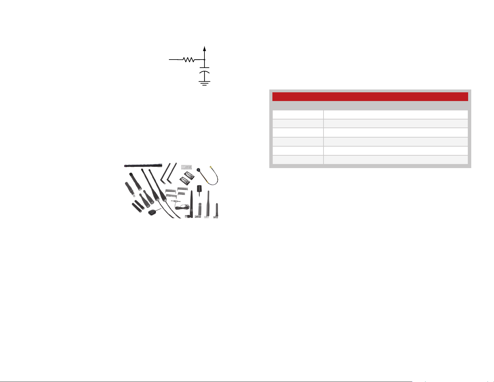
Figure 37: Supply Filter
A 10Ω resistor in series with the supply followed by a 10µF tantalum
capacitor from Vcc to ground helps in cases where the quality of supply
power is poor (Figure 37). This filter should be placed close to the module’s
supply lines. These values may need to be adjusted depending on the
noise present on the supply line.
Vcc TO
MODULE
10Ω
+
10µF
Antenna Considerations
The choice of antennas is a
critical and often overlooked
design consideration. The range,
performance and legality of an RF
link are critically dependent upon the
antenna. While adequate antenna
performance can often be obtained
by trial and error methods, antenna
design and matching is a complex
task. Professionally designed antennas such as those from Linx (Figure
38) help ensure maximum performance and FCC and other regulatory
compliance.
Figure 38: Linx Antennas
Helpful Application Notes from Linx
It is not the intention of this manual to address in depth many of the issues
that should be considered to ensure that the modules function correctly
and deliver the maximum possible performance. We recommend reading
the application notes listed in Figure 39 which address in depth key areas
of RF design and application of Linx products. These applications notes
are available online at www.linxtechnologies.com or by contacting the Linx
literature department.
Helpful Application Note Titles
Note Number Note Title
AN-00100 RF 101: Information for the RF Challenged
AN-00126 Considerations for Operation Within the 902–928MHz Band
AN-00130 Modulation Techniques for Low-Cost RF Data Links
AN-00140 The FCC Road: Part 15 from Concept to Approval
AN-00500 Antennas: Design, Application, Performance
AN-00501 Understanding Antenna Specifications and Operation
Figure 39: Helpful Application Note Titles
Linx transmitter modules typically have an output power that is higher
than the legal limits. This allows the designer to use an inefficient antenna
such as a loop trace or helical to meet size, cost or cosmetic requirements
and still achieve full legal output power for maximum range. If an efficient
antenna is used, then some attenuation of the output power will likely be
needed.
It is usually best to utilize a basic quarter-wave whip until your prototype
product is operating satisfactorily. Other antennas can then be evaluated
based on the cost, size and cosmetic requirements of the product.
Additional details are in Application Note AN-00500.
– –
30 31
– –
Page 19
0.070
0.060
0.070
0.095
Interference Considerations
The RF spectrum is crowded and the potential for conflict with unwanted
sources of RF is very real. While all RF products are at risk from
interference, its effects can be minimized by better understanding its
characteristics.
Interference may come from internal or external sources. The first step
is to eliminate interference from noise sources on the board. This means
paying careful attention to layout, grounding, filtering and bypassing in
order to eliminate all radiated and conducted interference paths. For
many products, this is straightforward; however, products containing
components such as switching power supplies, motors, crystals and other
potential sources of noise must be approached with care. Comparing your
own design with a Linx evaluation board can help to determine if and at
what level design-specific interference is present.
External interference can manifest itself in a variety of ways. Low-level
interference produces noise and hashing on the output and reduces the
link’s overall range.
High-level interference is caused by nearby products sharing the same
frequency or from near-band high-power devices. It can even come from
your own products if more than one transmitter is active in the same area.
It is important to remember that only one transmitter at a time can occupy
a frequency, regardless of the coding of the transmitted signal. This type of
interference is less common than those mentioned previously, but in severe
cases it can prevent all useful function of the affected device.
Although technically not interference, multipath is also a factor to be
understood. Multipath is a term used to refer to the signal cancellation
effects that occur when RF waves arrive at the receiver in different phase
relationships. This effect is a particularly significant factor in interior
environments where objects provide many different signal reflection paths.
Multipath cancellation results in lowered signal levels at the receiver and
shorter useful distances for the link.
Pad Layout
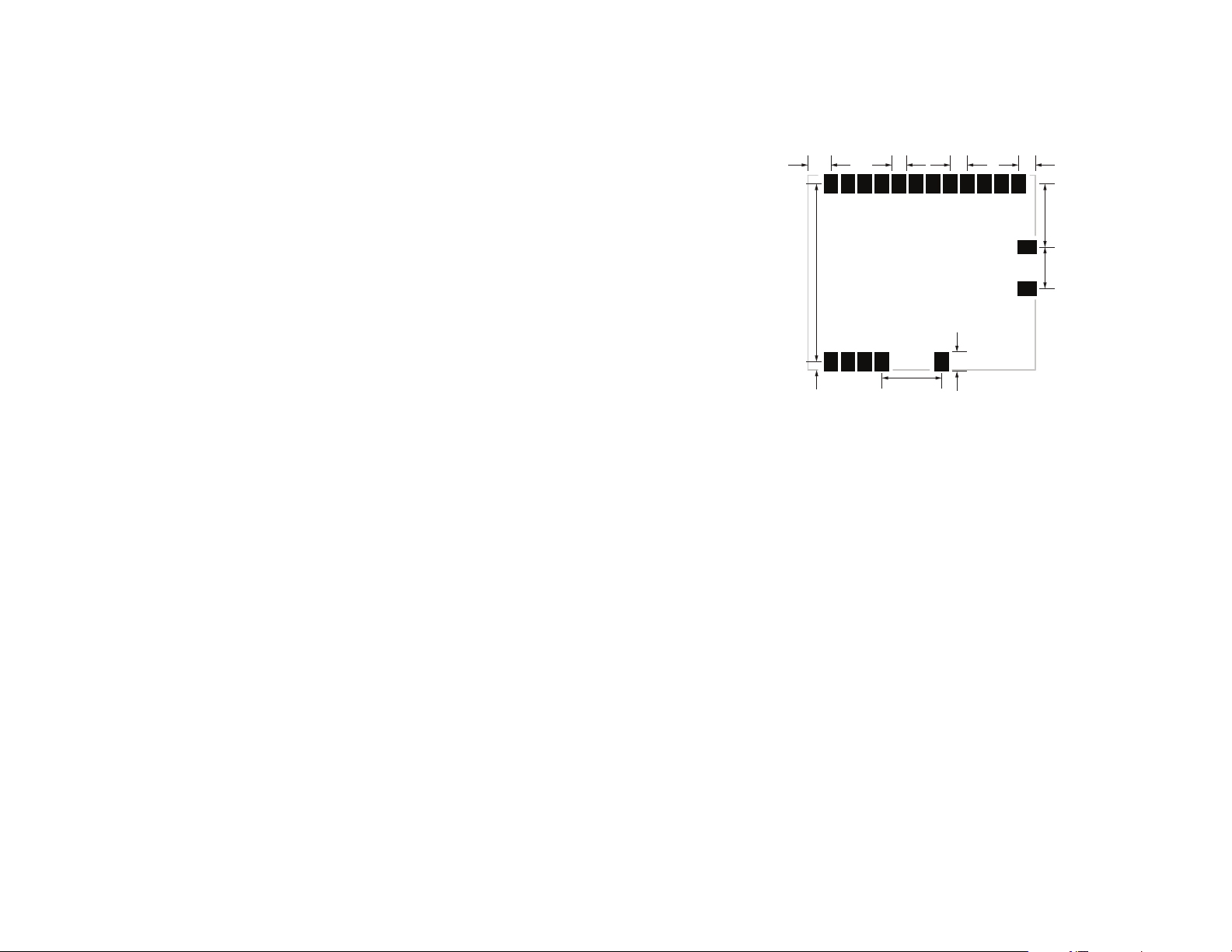
The pad layout diagram in Figure 40 is designed to facilitate both hand and
automated assembly.
0.245
(1.78mm)
(2.03mm)
(1.78mm)
0.295
(7.49mm)
0.170
(4.32mm)
0.080
(2.41mm)
0.730
(18.54mm)
0.035
(0.89mm)
Figure 40: Recommended PCB Layout
(1.52mm)
(6.22mm)
Board Layout Guidelines
The module’s design makes integration straightforward; however, it
is still critical to exercise care in PCB layout. Failure to observe good
layout techniques can result in a significant degradation of the module’s
performance. A primary layout goal is to maintain a characteristic
50-ohm impedance throughout the path from the antenna to the module.
Grounding, filtering, decoupling, routing and PCB stack-up are also
important considerations for any RF design. The following section provides
some basic design guidelines.
During prototyping, the module should be soldered to a properly laid-out
circuit board. The use of prototyping or “perf” boards results in poor
performance and is strongly discouraged. Likewise, the use of sockets
can have a negative impact on the performance of the module and is
discouraged.
The module should, as much as reasonably possible, be isolated from
other components on your PCB, especially high-frequency circuitry such as
crystal oscillators, switching power supplies, and high-speed bus lines.
When possible, separate RF and digital circuits into different PCB regions.
– –
32 33
– –
Page 20
Make sure internal wiring is routed away from the module and antenna and
is secured to prevent displacement.
Do not route PCB traces directly under the module. There should not be
any copper or traces under the module on the same layer as the module,
just bare PCB. The underside of the module has traces and vias that could
short or couple to traces on the product’s circuit board.
The Pad Layout section shows a typical PCB footprint for the module. A
ground plane (as large and uninterrupted as possible) should be placed on
a lower layer of your PC board opposite the module. This plane is essential
for creating a low impedance return for ground and consistent stripline
performance.
Use care in routing the RF trace between the module and the antenna
or connector. Keep the trace as short as possible. Do not pass it under
the module or any other component. Do not route the antenna trace on
multiple PCB layers as vias add inductance. Vias are acceptable for tying
together ground layers and component grounds and should be used in
multiples.
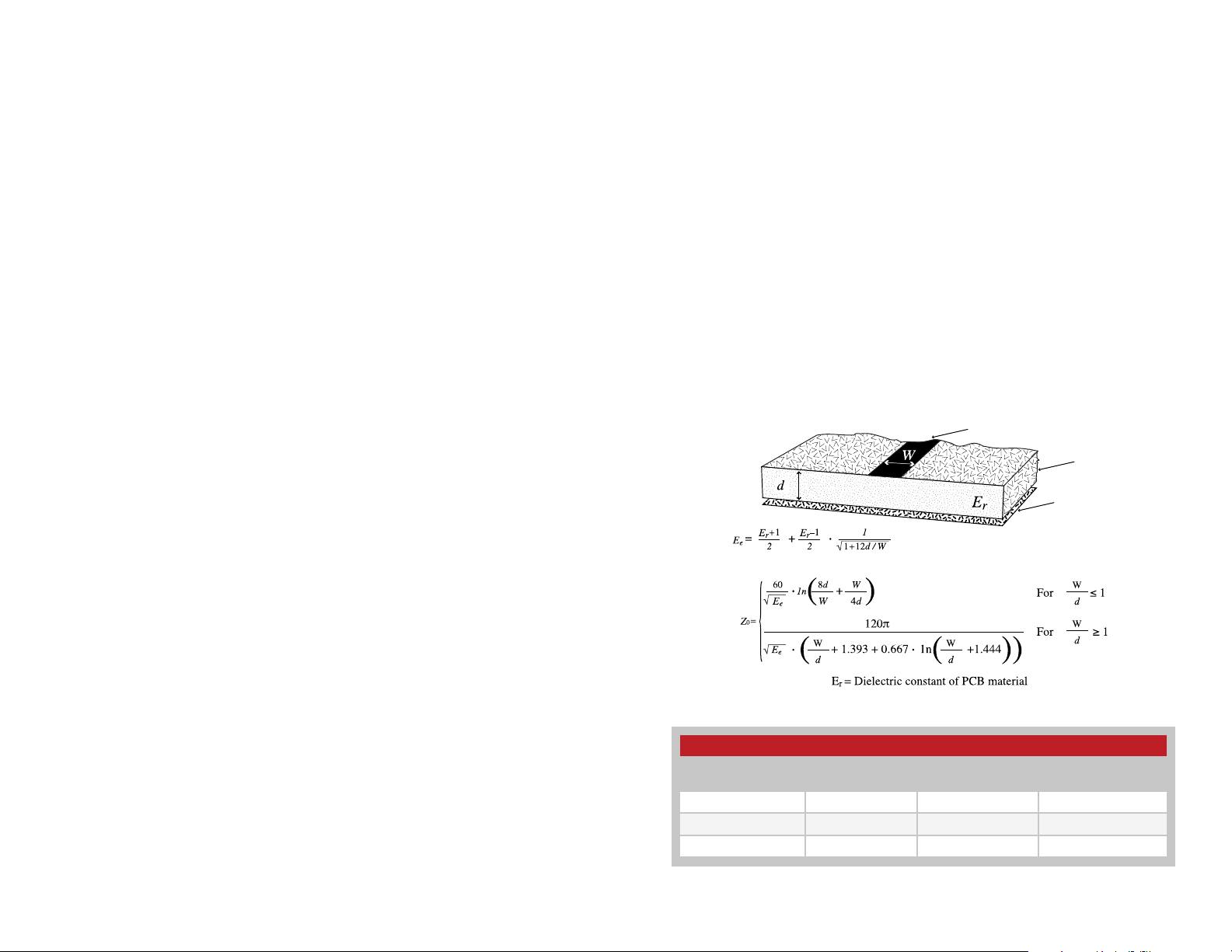
Microstrip Details
A transmission line is a medium whereby RF energy is transferred from
one place to another with minimal loss. This is a critical factor, especially
in high-frequency products like Linx RF modules, because the trace
leading to the module’s antenna can effectively contribute to the length
of the antenna, changing its resonant bandwidth. In order to minimize
loss and detuning, some form of transmission line between the antenna
and the module should be used unless the antenna can be placed very
close (<1/8in) to the module. One common form of transmission line is a
coax cable and another is the microstrip. This term refers to a PCB trace
running over a ground plane that is designed to serve as a transmission line
between the module and the antenna. The width is based on the desired
characteristic impedance of the line, the thickness of the PCB and the
dielectric constant of the board material. For standard 0.062in thick FR-4
board material, the trace width would be 111 mils. The correct trace width
can be calculated for other widths and materials using the information in
Figure 41 and examples are provided in Figure 42. Software for calculating
microstrip lines is also available on the Linx website.
Trace
Board
Each of the module’s ground pins should have short traces tying
immediately to the ground plane through a via.
Bypass caps should be low ESR ceramic types and located directly
adjacent to the pin they are serving.
A 50-ohm coax should be used for connection to an external antenna.
A 50-ohm transmission line, such as a microstrip, stripline or coplanar
waveguide should be used for routing RF on the PCB. The Microstrip
Details section provides additional information.
In some instances, a designer may wish to encapsulate or “pot” the
product. There are a wide variety of potting compounds with varying
dielectric properties. Since such compounds can considerably impact
RF performance and the ability to rework or service the product, it is
the responsibility of the designer to evaluate and qualify the impact and
suitability of such materials.
– –
34 35
Figure 41: Microstrip Formulas
Example Microstrip Calculations
Dielectric Constant
4.80 1.8 3.59 50.0
4.00 2.0 3.07 51.0
2.55 3.0 2.12 48.8
Figure 42: Example Microstrip Calculations
Width / Height
Ratio (W / d)
Effective Dielectric
Constant
– –
Ground plane
Characteristic
Impedance (Ω)
Page 21
Production Guidelines
300
The module is housed in a hybrid SMD package that supports hand and
automated assembly techniques. Since the modules contain discrete
components internally, the assembly procedures are critical to ensuring
the reliable function of the modules. The following procedures should be
reviewed with and practiced by all assembly personnel.
Hand Assembly
Pads located on the bottom
of the module are the primary
mounting surface (Figure 43).
Since these pads are inaccessible
during mounting, castellations
that run up the side of the module
have been provided to facilitate
solder wicking to the module’s
underside. This allows for very
quick hand soldering for prototyping and small volume production. If the
recommended pad guidelines have been followed, the pads will protrude
slightly past the edge of the module. Use a fine soldering tip to heat the
board pad and the castellation, then introduce solder to the pad at the
module’s edge. The solder will wick underneath the module, providing
reliable attachment. Tack one module corner first and then work around the
device, taking care not to exceed the times in Figure 44.
Soldering Iron
Tip
Solder
PCB Pads
Figure 43: Soldering Technique
Castellations
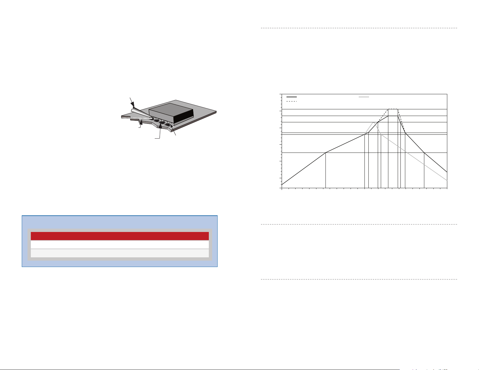
Reflow Temperature Profile
The single most critical stage in the automated assembly process is the
reflow stage. The reflow profile in Figure 45 should not be exceeded
because excessive temperatures or transport times during reflow will
irreparably damage the modules. Assembly personnel need to pay careful
attention to the oven’s profile to ensure that it meets the requirements
necessary to successfully reflow all components while still remaining
within the limits mandated by the modules. The figure below shows the
recommended reflow oven profile for the modules.
Recommended RoHS Profile
Max RoHS Profile
255°C
250
235°C
217°C
200
185°C
C)
o
180°C
150
125°C
Temperature (
100
50
60 12030 150180 210240 270300 330360090
Figure 45: Maximum Reflow Temperature Profile
Time (Seconds)
Recommended Non-RoHS Profile
Warning: Pay attention to the absolute maximum solder times.
Absolute Maximum Solder Times
Hand Solder Temperature: +427ºC for 10 seconds for lead-free alloys
Reflow Oven: +255ºC max (see Figure 45)
Figure 44: Absolute Maximum Solder Times
Automated Assembly
For high-volume assembly, the modules are generally auto-placed.
The modules have been designed to maintain compatibility with reflow
processing techniques; however, due to their hybrid nature, certain aspects
of the assembly process are far more critical than for other component
types. Following are brief discussions of the three primary areas where
caution must be observed.
– –
36 37
Shock During Reflow Transport
Since some internal module components may reflow along with the
components placed on the board being assembled, it is imperative that
the modules not be subjected to shock or vibration during the time solder
is liquid. Should a shock be applied, some internal components could be
lifted from their pads, causing the module to not function properly.
Washability
The modules are wash-resistant, but are not hermetically sealed. Linx
recommends wash-free manufacturing; however, the modules can be
subjected to a wash cycle provided that a drying time is allowed prior
to applying electrical power to the modules. The drying time should be
sufficient to allow any moisture that may have migrated into the module
to evaporate, thus eliminating the potential for shorting damage during
power-up or testing. If the wash contains contaminants, the performance
may be adversely affected, even after drying.
– –
Page 22
General Antenna Rules
OPTIMUM
USABLE
NOT RECOMMENDED
The following general rules should help in maximizing antenna performance.
1. Proximity to objects such as a user’s hand, body or metal objects will
cause an antenna to detune. For this reason, the antenna shaft and tip
should be positioned as far away from such objects as possible.
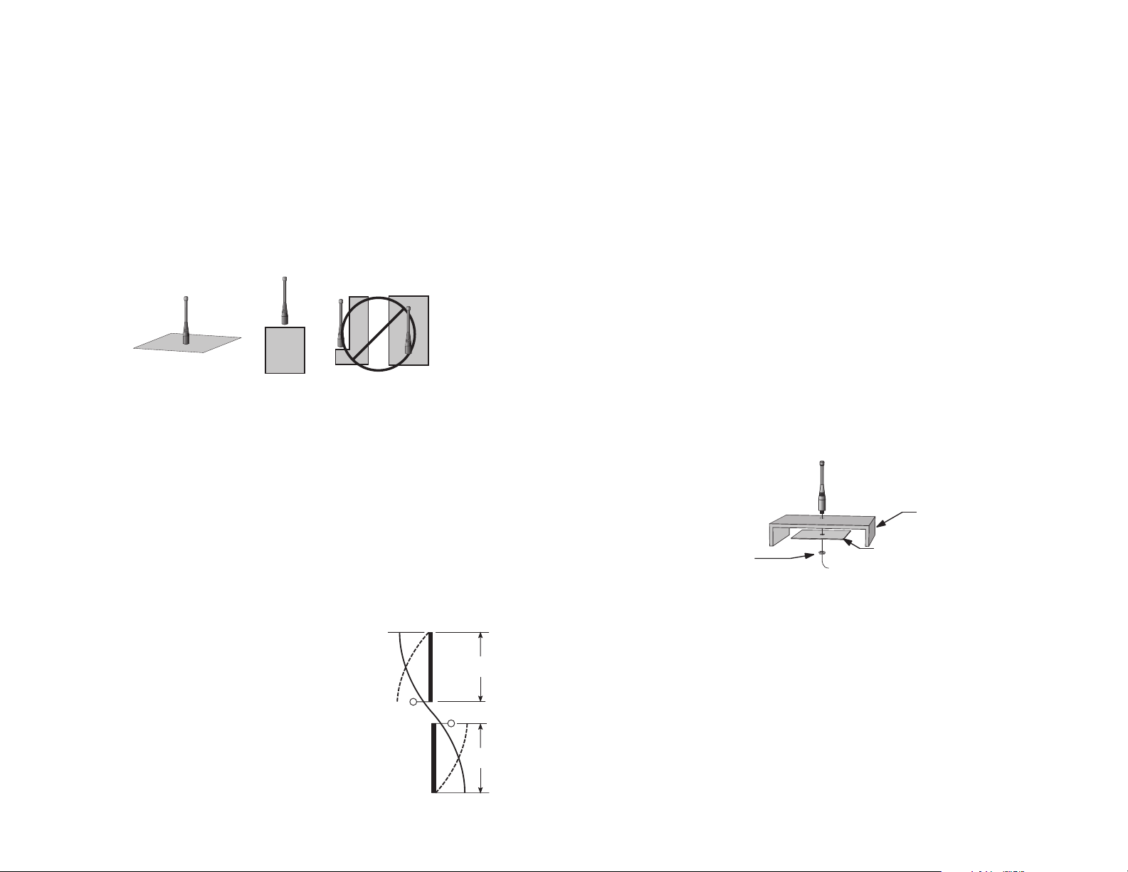
2. Optimum performance is obtained from a ¼- or ½-wave straight whip
mounted at a right angle to the ground plane (Figure 46). In many
cases, this isn’t desirable for practical or ergonomic reasons, thus,
an alternative antenna style such as a helical, loop or patch may be
utilized and the corresponding sacrifice in performance accepted.
plane as possible in proximity to the base of the antenna. In cases
where the antenna is remotely located or the antenna is not in close
proximity to a circuit board, ground plane or grounded metal case, a
metal plate may be used to maximize the antenna’s performance.
5. Remove the antenna as far as possible from potential interference
sources. Any frequency of sufficient amplitude to enter the receiver’s
front end will reduce system range and can even prevent reception
entirely. Switching power supplies, oscillators or even relays can also
be significant sources of potential interference. The single best weapon
against such problems is attention to placement and layout. Filter the
module’s power supply with a high-frequency bypass capacitor. Place
adequate ground plane under potential sources of noise to shunt noise
to ground and prevent it from coupling to the RF stage. Shield noisy
board areas whenever practical.
OPTIMUM
USABLE
Figure 46: Ground Plane Orientation
NOT RECOMMENDED
3. If an internal antenna is to be used, keep it away from other metal
components, particularly large items like transformers, batteries,
PCB tracks and ground planes. In many cases, the space around the
antenna is as important as the antenna itself. Objects in close proximity
to the antenna can cause direct detuning, while those farther away will
alter the antenna’s symmetry.
4. In many antenna designs, particularly ¼-wave whips, the ground plane
acts as a counterpoise, forming, in essence,
a ½-wave dipole (Figure 47). For this reason,
adequate ground plane area is essential.
The ground plane can be a metal case or
ground-fill areas on a circuit board. Ideally, it
should have a surface area less than or equal
to the overall length of the ¼-wave radiating
element. This is often not practical due to
size and configuration constraints. In these
instances, a designer must make the best use
VERTICAL λ/4 GROUNDED
ANTENNA (MARCONI)
E
I
GROUND
VIRTUAL λ/4
DIPOLE
PLANE
DIPOLE
ELEMENT
λ/4
λ/4
of the area available to create as much ground
6. In some applications, it is advantageous to place the module and
antenna away from the main equipment (Figure 48). This can avoid
interference problems and allows the antenna to be oriented for
optimum performance. Always use 50Ω coax, like RG-174, for the
remote feed.
CASE
NUT
Figure 48: Remote Ground Plane
GROUND PLANE
(MAY BE NEEDED)
Figure 47: Dipole Antenna
– –
38 39
– –
Page 23
Common Antenna Styles
There are hundreds of antenna styles and variations that can be employed
with Linx RF modules. Following is a brief discussion of the styles most
commonly utilized. Additional antenna information can be found in Linx
Application Notes AN-00100, AN-00140, AN-00500 and AN-00501. Linx
antennas and connectors offer outstanding performance at a low price.
Whip Style
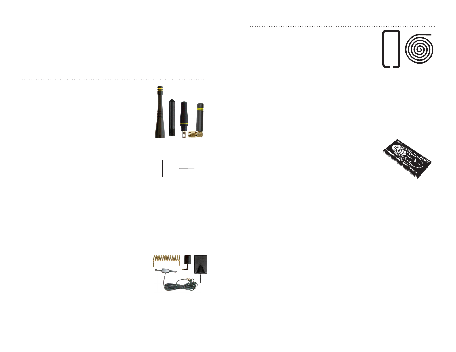
A whip style antenna (Figure 49) provides
outstanding overall performance and stability.
A low-cost whip can be easily fabricated from
a wire or rod, but most designers opt for the
consistent performance and cosmetic appeal of
a professionally-made model. To meet this need,
Linx offers a wide variety of straight and reduced
height whip style antennas in permanent and
connectorized mounting styles.
The wavelength of the operational frequency determines
an antenna’s overall length. Since a full wavelength
is often quite long, a partial ½- or ¼-wave antenna
is normally employed. Its size and natural radiation
resistance make it well matched to Linx modules.
The proper length for a straight ¼-wave can be easily
determined using the formula in Figure 50. It is also
possible to reduce the overall height of the antenna by
using a helical winding. This reduces the antenna’s bandwidth but is a great
way to minimize the antenna’s physical size for compact applications. This
also means that the physical appearance is not always an indicator of the
antenna’s frequency.
Figure 49: Whip Style Antennas
234
L =
F
MHz
Figure 50:
L = length in feet of
quarter-wave length
F = operating frequency
in megahertz
Loop Style
A loop or trace style antenna is normally printed
directly on a product’s PCB (Figure 52). This
makes it the most cost-effective of antenna
styles. The element can be made self-resonant or
externally resonated with discrete components,
but its actual layout is usually product specific.
Despite the cost advantages, loop style antennas
Figure 52: Loop or Trace Antenna
are generally inefficient and useful only for short
range applications. They are also very sensitive to changes in layout and
PCB dielectric, which can cause consistency issues during production.
In addition, printed styles are difficult to engineer, requiring the use of
expensive equipment including a network analyzer. An improperly designed
loop will have a high VSWR at the desired frequency which can cause
instability in the RF stage.
Linx offers low-cost planar (Figure 53) and chip
antennas that mount directly to a product’s PCB.
These tiny antennas do not require testing and
provide excellent performance despite their small
size. They offer a preferable alternative to the often
problematic “printed” antenna.
Figure 53: SP Series
“Splatch” Antenna
Specialty Styles
Linx offers a wide variety of specialized antenna
styles (Figure 51). Many of these styles utilize helical
elements to reduce the overall antenna size while
maintaining reasonable performance. A helical
antenna’s bandwidth is often quite narrow and the
antenna can detune in proximity to other objects, so
care must be exercised in layout and placement.
– –
40 41
Figure 51: Specialty Style
Antennas
– –
Page 24

Regulatory Considerations
Note: Linx RF modules are designed as component devices that require
external components to function. The purchaser understands that
additional approvals may be required prior to the sale or operation of
the device, and agrees to utilize the component in keeping with all laws
governing its use in the country of operation.
When working with RF, a clear distinction must be made between what
is technically possible and what is legally acceptable in the country where
operation is intended. Many manufacturers have avoided incorporating RF
into their products as a result of uncertainty and even fear of the approval
and certification process. Here at Linx, our desire is not only to expedite the
design process, but also to assist you in achieving a clear idea of what is
involved in obtaining the necessary approvals to legally market a completed
product.
For information about regulatory approval, read AN-00142 on the Linx
website or call Linx. Linx designs products with worldwide regulatory
approval in mind.
Questions regarding interpretations of the Part 2 and Part 15 rules or the
measurement procedures used to test intentional radiators such as Linx RF
modules for compliance with the technical standards of Part 15 should be
addressed to:
Federal Communications Commission
Equipment Authorization Division
Customer Service Branch, MS 1300F2
7435 Oakland Mills Road
Columbia, MD, US 21046
Phone: + 1 301 725 585 | Fax: + 1 301 344 2050
Email: [email protected]
ETSI Secretaria
650, Route des Lucioles
06921 Sophia-Antipolis Cedex
FRANCE
Phone: +33 (0)4 92 94 42 00
Fax: +33 (0)4 93 65 47 16
In the United States, the approval process is actually quite straightforward.
The regulations governing RF devices and the enforcement of them are
the responsibility of the Federal Communications Commission (FCC). The
regulations are contained in Title 47 of the United States Code of Federal
Regulations (CFR). Title 47 is made up of numerous volumes; however,
all regulations applicable to this module are contained in Volume 0-19.
It is strongly recommended that a copy be obtained from the FCC’s
website, the Government Printing Office in Washington or from your local
government bookstore. Excerpts of applicable sections are included
with Linx evaluation kits or may be obtained from the Linx Technologies
website, www.linxtechnologies.com. In brief, these rules require that any
device that intentionally radiates RF energy be approved, that is, tested for
compliance and issued a unique identification number. This is a relatively
painless process. Final compliance testing is performed by one of the many
independent testing laboratories across the country. Many labs can also
provide other certifications that the product may require at the same time,
such as UL, CLASS A / B, etc. Once the completed product has passed,
an ID number is issued that is to be clearly placed on each product
manufactured.
International approvals are slightly more complex, although Linx modules
are designed to allow all international standards to be met. If the end
product is to be exported to other countries, contact Linx to determine the
specific suitability of the module to the application.
All Linx modules are designed with the approval process in mind and thus
much of the frustration that is typically experienced with a discrete design is
eliminated. Approval is still dependent on many factors, such as the choice
of antennas, correct use of the frequency selected and physical packaging.
While some extra cost and design effort are required to address these
issues, the additional usefulness and profitability added to a product by RF
makes the effort more than worthwhile.
– –
42 43
– –
Page 25

Linx Technologies
159 Ort Lane
Merlin, OR, US 97532
Phone: +1 541 471 6256
Fax: +1 541 471 6251
www.linxtechnologies.com
Disclaimer
Linx Technologies is continually striving to improve the quality and function of its products. For this reason, we
reserve the right to make changes to our products without notice. The information contained in this Data Guide
is believed to be accurate as of the time of publication. Specifications are based on representative lot samples.
Values may vary from lot-to-lot and are not guaranteed. “Typical” parameters can and do vary over lots and
application. Linx Technologies makes no guarantee, warranty, or representation regarding the suitability of any
product for use in any specific application. It is the customer’s responsibility to verify the suitability of the part for
the intended application. NO LINX PRODUCT IS INTENDED FOR USE IN ANY APPLICATION WHERE THE SAFETY
OF LIFE OR PROPERTY IS AT RISK.
Linx Technologies DISCLAIMS ALL WARRANTIES OF MERCHANTABILITY AND FITNESS FOR A PARTICULAR
PURPOSE. IN NO EVENT SHALL LINX TECHNOLOGIES BE LIABLE FOR ANY OF CUSTOMER’S INCIDENTAL OR
CONSEQUENTIAL DAMAGES ARISING IN ANY WAY FROM ANY DEFECTIVE OR NON-CONFORMING PRODUCTS
OR FOR ANY OTHER BREACH OF CONTRACT BY LINX TECHNOLOGIES. The limitations on Linx Technologies’
liability are applicable to any and all claims or theories of recovery asserted by Customer, including, without
limitation, breach of contract, breach of warranty, strict liability, or negligence. Customer assumes all liability
(including, without limitation, liability for injury to person or property, economic loss, or business interruption) for
all claims, including claims from third parties, arising from the use of the Products. The Customer will indemnify,
defend, protect, and hold harmless Linx Technologies and its officers, employees, subsidiaries, affiliates,
distributors, and representatives from and against all claims, damages, actions, suits, proceedings, demands,
assessments, adjustments, costs, and expenses incurred by Linx Technologies as a result of or arising from any
Products sold by Linx Technologies to Customer. Under no conditions will Linx Technologies be responsible for
losses arising from the use or failure of the device in any application, other than the repair, replacement, or refund
limited to the original product purchase price. Devices described in this publication may contain proprietary,
patented, or copyrighted techniques, components, or materials. Under no circumstances shall any user be
conveyed any license or right to the use or ownership of such items.
©2015 Linx Technologies. All rights reserved.
The stylized Linx logo, Wireless Made Simple, WiSE, CipherLinx and the stylized CL logo are trademarks of Linx Technologies.
 Loading...