L DESIGN IDEAS
5V TO 15V
5V, 0.2A
T1
Primary-Side Sensing Takes
Complexity out of Isolated
Flyback Converter Design
Introduction
Flyback converters are widely used
in isolated DC/DC applications, but
they are not necessarily a designer’s
first choice. Power supply designers grudgingly choose a flyback out
of necessity for electronic isolation;
certainly not because they are an
easy to design. A flyback converter
requires that significant design time
be devoted to transformer design, a
task further complicated by limited
off-the-shelf transformer selection and
the necessity for customized magnetics. Moreover, the flyback converter
has stability issues due to the wellknown right-half-plane (RHP) zero
in the control loop, which is further
complicated by the propagation delay
of an optocoupler.
The LT3573 isolated monolithic
flyback converter solves many of the
design difficulties commonly associ-
DESIGN IDEAS
Primary-Side Sensing Takes
Complexity out of Isolated
Flyback Converter Design ..................30
Tiger Zhou
Easy Automotive Power Supplies:
Compact Regulator Produces
Dual Outputs as Low as 0.8V from
3.6V–36V and is Unfazed by
60V Transients..................................32
Peter J. Andrews
High Power 2-Phase Synchronous
Boost Replaces Hot Diodes with
Cool FETs—No Heat Sinks Required
.........................................................35
Narayan Raja, Tuan Nguyen
and Theo Phillips
100V Controller in 3mm × 3mm
QFN or MSE Drives High Power
LED Strings from Just About
Any Input ..........................................37
Keith Szolusha
Parallel Buck-Boost µModule
Regulators to Produce High Current
in Sub-2.8mm Height Applications
.........................................................40
Judy Sun, Sam Young and Henry Zhang
V
IN
4.7
µF
200k
SHDN/UVLO
90.9k
TC
R
ILIM
SS
10k
20k
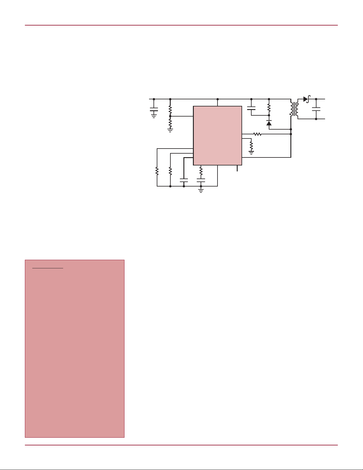
Figure 1. Amazingly simple flyback converter takes advantage of the primary side sensing
scheme of the LT3573. Note the absence of an optocoupler. Also note the tiny coupling inductor
available from many magnetics vendors.
0.01µF
V
IN
LT3573
VC GND BIAS
24.9k
2.2nF
ated with flyback converters by using
a primary-side sensing scheme that is
capable of detecting the output voltage
through the flyback switching node
waveform. During the switch off-period, the diode delivers the current to
the output, and the output voltage is
thus reflected to the primary-side of
the flyback transformer (or the switch
node). The magnitude of the switch
node voltage is the summation of the
input voltage and reflected output
voltage. The flyback converter is able
to reconstruct the output voltage from
the measurement of the switching
node voltage during the off period.
This scheme has previously proven
itself in Linear Technology’s family
of photoflash capacitor charger ICs.
Design is simplified by getting rid of
the optocoupler while maintaining
the galvanic isolation between the
primary-side and secondary-side of
the transformer.
The LT3573’s utilization of boundary mode operation further reduces
converter size and simplifies system
design. The flyback converter turns
on the 1.25A, 60V internal switch
right after the secondary diode current reduces to zero, while it turns
by Tiger Zhou
D1
1:1
T1
2k
0.22µF
D2
R
R
REF
SW
V
27.4k
FB
6.04k
T1: BH ELECTRONICS, L10-1022
D1: B240A
IN
D2: 1N4148W
off when the switch current reaches
the pre-defined current limit. Thus it
always operates at the transition of
continuous conduction mode (CCM)
and discontinuous conduction mode
(DCM), which is called boundary mode.
Boundary mode operation also offers
a superior load regulation.
Other features, such as soft-start,
adjustable current limit, undervoltage
lockout and temperature compensation further facilitate the flyback
converter design. Figure 1 shows
a simple flyback converter using
LT3573.
Primary-Side Sensing
Needs No Optocoupler
An optocoupler is essential for a traditional flyback converter. It transmits
the output voltage feedback signal
through an optical link while maintaining an isolation barrier. However,
the optocoupler current transfer ratio
(CTR) often changes with temperature,
degrading accuracy. Also, the optocoupler causes a propagation delay,
which impacts the dynamic response
of the control loop.
The LT3573 eliminates the need for
an optocoupler by sensing the output
V
OUT
47
µF
V
OUT
+
–
30
30
Linear Technology Magazine • January 2009

1
1
1
9V TO 30V
5V, 1A
SW VOLTAGE
SW CURRENT
DIODE CURRENT
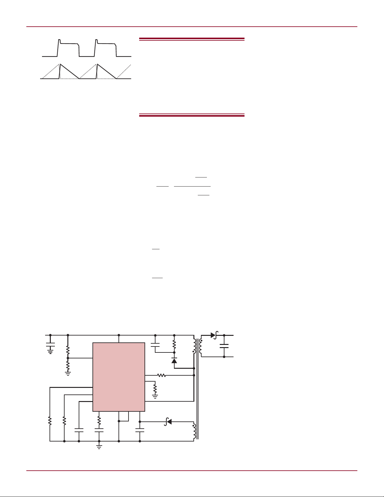
Figure 2. LT3573 flyback
converter in boundary mode.
voltage on the primary-side. The output voltage is accurately measured at
the primary-side switching node waveform during the off period. In addition
to the obvious simplification and cost
savings of this design, this scheme
improves dynamic performance during
load transients, which further simplifies the control loop design.
Boundary Mode Operation
Reduces Converter Size and
Simplifies System Design
Since the flyback converter operates in
boundary mode, the switch is always
turned on at zero current and the diode
has no reverse recovery loss. Reducing
power losses allows the flyback converter to operate at a relatively high
switching frequency, which in turn
reduces the transformer size when
compared to lower frequency operation. Figure 1 shows an isolated flyback
using a small coupling inductor with
19µH primary inductance.
Another benefit of boundary mode
operation is a simplified control loop.
V
IN
4.7
µF
357k
SHDN/UVLO
51.1k
TC
R
ILIM
SS
VC GND BIAS
20k 10k
Linear Technology Magazine • January 2009
0.01µF
Figure 3. A 9V–30V input, 5V/1A flyback converter with
a BIAS winding to maximize the system efficiency.
V
LT3573
24.9k
2.2nF
DESIGN IDEAS L
The simplified control loop network
The LT3573 simplifies the
design of flyback converters
by using a primary-side
sensing scheme that detects
the output voltage through
the flyback switching node
waveform.
Figure 2 shows the LT3573 flyback
converter voltage and current waveform in boundary mode. Assuming a
1:1 transformer is used; the controlto-output transfer function is:
R R
+
C
1
G
=
VC
D
−
•
2
+ +
R R
C
Where R is the load resistor, C is
the output capacitor, RC is the ESR of
the output capacitor and D is the duty
cycle. From this, a load pole at
s
=
p
RC
and ESR zero at
s
=
z
R C
C
are observed. This reduced-order
transfer function can be easily compensated by an external VC network.
0.22µF
IN
84.5k
FB
6.04k
1µF
TEST
R
R
REF
SW
2k
D2
D3
s C
•
1
•
s C
T1
D1
3:1:1
D1: B340A
D2: 1N4148W
D3: CMDSH-3
T1: PULSE PA2454NL
47
also eases transformer design. The
control-to-output transfer function
has no inductance component, which
means the flyback converter easily
tolerates transformer variations. The
transformer inductance only affects
the converter switching frequency; it
does not affect the converter output
capability and stability. The data sheet
includes a detailed design example,
which outlines converter design
guidelines.
Boundary Mode Operation for
Superior Load Regulation
Since the diode voltage drop is included
in the reflected output voltage, it can
affect load regulation in primary-side
sensing flyback converters that operate in CCM. The reason is the diode
has nonlinear I-V characteristics.
Other methods such as load regulation compensation must be used if
a tight load regulation is required.
However, the load regulation is much
improved in boundary mode operation
because the reflected output voltage is always sampled at the diode
current zero-crossing. The LT3573
flyback converter has a typical 1%
load regulation.
Figure 3 shows a 5V, 1A flyback
converter that accepts a 9V to 30V
input. The BIAS winding is used to
improve the system efficiency. The
TC resistor compensates the output
voltage at all temperatures, the UVLO
resistors set the intended input range,
V
and the current limit resistor programs
OUT
the output current.
µF
Conclusion
COM
The LT3573 simplifies the design of
isolated flyback converters with a
primary-side sensing scheme and
boundary mode operation. Its wide
3V to 40V input range, and its ability to deliver 7W output power make
it suitable for industrial, automotive
and medical applications. It also
includes undervoltage lockout, softstart, temperature compensation,
adjustable current limit and external
compensation.
L
3131
 Loading...