

Page 1
查询LTC3252供应商
FEATURES
LTC3252
Dual, Low Noise,
Inductorless Step-Down
DC/DC Converter
U
DESCRIPTIO
■
2.7V to 5.5V Input Voltage Range
■
No Inductors
■
Typical Efficiency 50% Higher than LDOs
■
Spread Spectrum Operation
■
Low Input and Output Noise
■
Shutdown Disconnects Load from V
■
Dual Adjustable Independent Outputs
IN
(Range: 0.9V to 1.6V)
■
Output Current: 250mA Each Output
■
Low Operating Current: IIN = 60µA Typ
(35µA with One Output Enabled)
■
Low Shutdown Current: IIN = 0.01µA Typ
■
Soft-Start Limits Inrush Current at Turn On
■
Short Circuit and Over Temperature Protected
■
Available in 4mm × 3mm 12-Pin DFN Package
U
APPLICATIO S
■
Handheld Electronic Devices
■
Cellular Phones
■
Low Voltage Logic Supplies
■
DSP Power Supplies
■
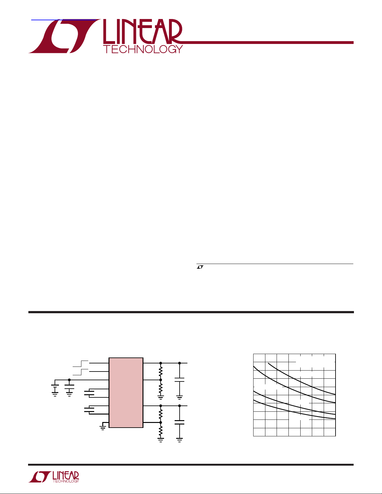
3.3V to 1.5V Conversion
The LTC®3252 is a switched capacitor step-down DC/DC
converter that produces two adjustable regulated outputs
from a single 2.7V to 5.5V input. The part uses switched
capacitor fractional conversion to achieve a typical efficiency increase of 50% over that of a linear regulator. No
inductors are required.
A unique constant frequency, spread spectrum architecture provides a very low noise regulated output as well as
low noise at the input. The part also has Burst Mode
®
operation to provide high efficiency at low output currents,
as well as ultralow current shutdown.
Low operating currents (60µA with both outputs enabled,
35µA with one output enabled) and low external parts
count make the LTC3252 ideally suited for space-constrained battery-powered applications. The part is shortcircuit and overtemperature protected and is available in a
tiny 4mm × 3mm 12-pin DFN package.
, LTC and LT are registered trademarks of Linear Technology Corporation.
Burst Mode is a registered trademark of Linear Technology Corporation.
TYPICAL APPLICATIO
1.5V and 1.2V Output Voltages with Shutdown
2
1µF
1µF
EN1
11
EN2
3
V
IN
4
+
C1
6
–
C1
10
+
C2
8
–
C2
7
GND
1-CELL
Li-ION
OR 3-CELL
NiMH
OFF ON
OFF ON
4.7µF
U
LTC3252
OUT1
FB1
OUT2
FB2
1.5V/1.2V Efficiency vs Input Voltage
5
470k
1
510k
9
261k
12
510k
V
I
OUT
4.7µF
V
I
OUT
4.7µF
= 1.5V
OUT
≤ 250mA
= 1.2V
OUT
≤ 250mA
3252 TA01
100
90
80
70
60
LTC3252-1.2V
50
40
EFFICIENCY (%)
30
20
10
0
3.1 3.5 3.9 4.3 4.7 5.1 5.5
2.7
I
(1.5V) = 100mA
OUT
(1.2V) = 100mA
I
OUT
LTC3252-1.5V
LDO-1.5V
LDO-1.2V
VIN (V)
3252 TA01a
3252f
1
Page 2
LTC3252
FB2
EN2
C2
+
OUT2
C2
–
GND
FB1
EN1
V
IN
C1
+
OUT1
C1
–
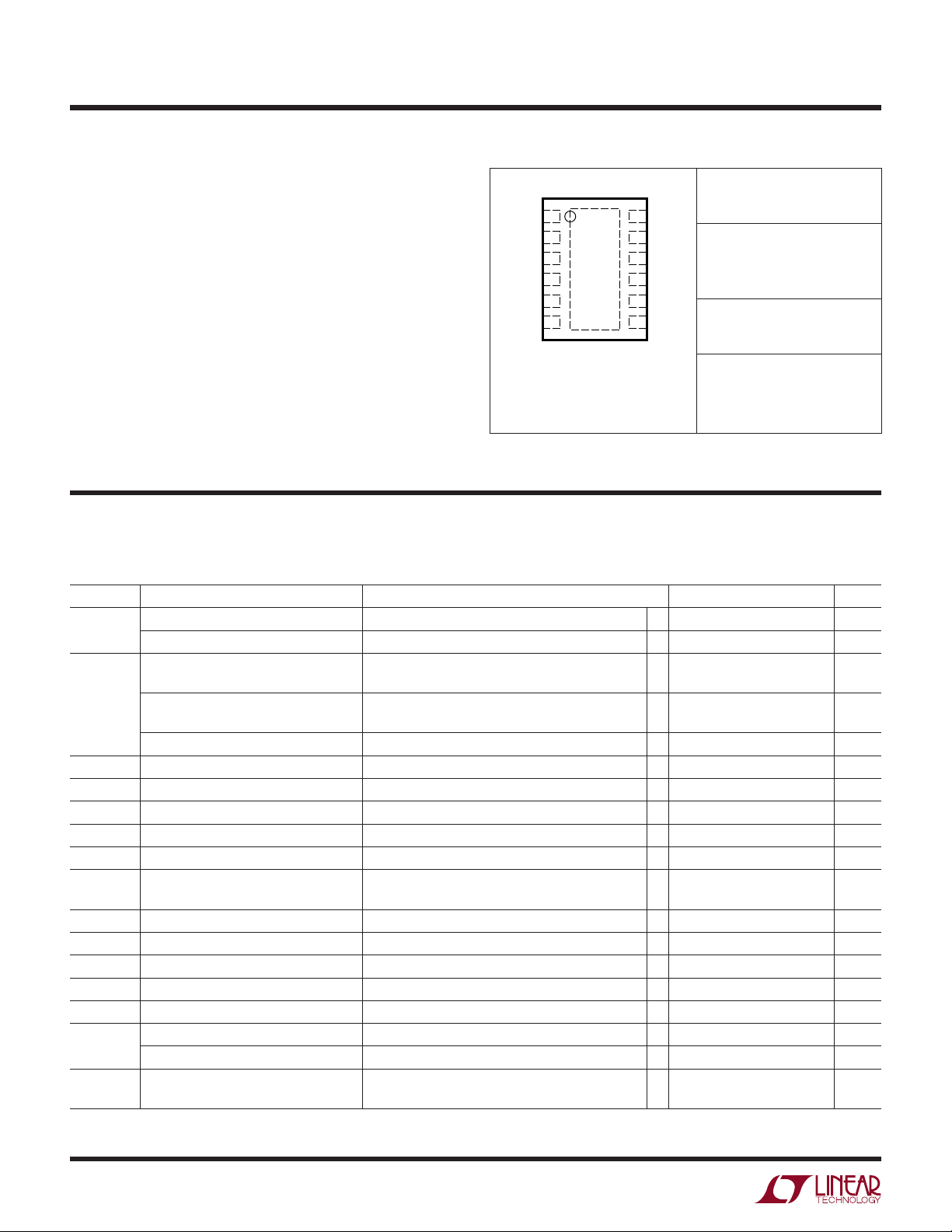
TOP VIEW
DE PACKAGE
12-LEAD (4mm × 3mm) PLASTIC DFN
12
11
10
9
8
7
1
2
3
4
5
6
WW
W
ABSOLUTE AXI U RATI GS
U
PACKAGE/ORDER I FOR ATIO
(Notes 1, 6)
VIN to GND................................................–0.3V to 6.0V
EN1, EN2, FB1, FB2 to GND .......... –0.3V to (VIN + 0.3V)
I
, I
OUT1
(Note 3)........................................... 400mA
OUT2
Operating Ambient Temperature Range
(Note 2) .................................................. – 40°C to 85°C
Storage Temperature Range ................. –65°C to 125°C
Lead Temperature (Soldering, 10 sec).................. 300°C
T
JMAX
Consult LTC Marketing for parts specified with wider operating temperature ranges.
ELECTRICAL CHARACTERISTICS
temperature range, otherwise specifications are at TA = 25°C. VIN = 3.6V, V
4.7µF (all capacitors ceramic) unless otherwise noted.
The ● denotes the specifications which apply over the full operating
EXPOSED PAD IS GROUND
(MUST BE SOLDERED TO PCB)
= 125°C, θJA = 40°C/W, θJC = 4.3°C/W
OUT1
= V
= 1.5V, C1 = C2 = 1µF, Cin = C
OUT2
UUW
ORDER PART
NUMBER
LTC3252EDE
DE PART
MARKING
3252
OUT1
= C
OUT2
=
SYMBOL PARAMETER CONDITIONS MIN TYP MAX UNITS
V
IN
Min Operating Voltage (Note 4) ● 2.7 V
Max Operating Voltage ● 5.5 V
I
VIN
Operating Current, I
Both Outputs Enabled 2.7V ≤ V
Operating Current, I
One Output Enabled V
Shutdown Current VM0 = 0V, VM1 = 0V, 2.7V ≤ VIN ≤ 5.5V ● 0.01 1 µA
V
FB1
I
OUT1
I
OUT2
I
FB
V
RIPPLE
, V
Feedback Voltage I
FB2
Output Current V
Output Current V
FB1, FB2 Input Current V
Output Ripple (OUT1 or OUT2) I
Spread Spectrum Frequency Range f
V
IH
V
IL
I
IH
I
IL
t
ON
OUT1, OUT2 Load Regulation (Referred to FB pin) 0.08 mV/mA
R
OL
2
EN1, EN2 Input High Voltage 2.7V ≤ VIN ≤ 5.5V ● 1.2 0.8 V
EN1, EN2 Input Low Voltage 2.7V ≤ VIN ≤ 5.5V ● 0.8 0.4 V
EN1, EN2 Input High Current EN1 = VIN, EN2 = V
EN1, EN2 Input Low Current EN1 = 0V, EN2 = 0V ● –1 1 µA
Turn On Time R
Line Regulation 0 ≤ I
Open Loop Output Impedance, VIN = 3.0V, I
(OUT1 or OUT2)
= 0mA, V
OUT
= 0mA, V
OUT
= 0, 2.7V ≤ V
EN2
= 0mA, 2.7V ≤ V
OUT
= V
EN1
= V
EN2
= V
FB1
FB2
= 250mA 10 mV
OUT
Switching Frequency ● 0.8 1.0 MHz
MIN
Switching Frequency ● 1.6 2.0 MHz
f
MAX
= 3Ω 0.8 ms
OUT
OUT1
IN
IN
IN
EN1
≤ 5.5V
EN1
= VIN, V
= 0, V
IN
= VIN, ● 60 100 µA
EN2
= VIN or V
EN2
= VIN, ● 35 60 µA
EN1
≤ 5.5V
≤ 5.5V ● 0.78 0.8 0.82 V
IN
● 250 mA
● 250 mA
= 0.85V ● –50 50 nA
IN
≤ 250mA or 0 ≤ I
= 200mA, VFB = 0.74V (Note 5) ● 1 1.4 Ω
OUT
≤ 250mA 0.2 %/V
OUT2
● –1 1 µA
P-P
3252f
Page 3
ELECTRICAL CHARACTERISTICS
LTC3252
Note 1: Absolute Maximum Ratings are those values beyond which the life
of a device may be impaired.
Note 2: The LTC3252EDE is guaranteed to meet specified performance
from 0°C to 70°C. Specifications over the –40°C and 85°C operating
temperature range are assured by design characterization and correlation
with statistical process control.
Note 3: Based on long-term current density limitations.
Note 4: Minimum operating voltage required for regulation is:
> 2 • (V
V
IN
Note 5: Output not in regulation; R
Note 6: This IC includes overtemperature protection that is intended to
protect the device during momentary overload conditions. Junction
temperature will exceed 125°C when overtemperature protection is active.
Continuous operation above the specified maximum operating junction
temperature may impair device reliability.
UW
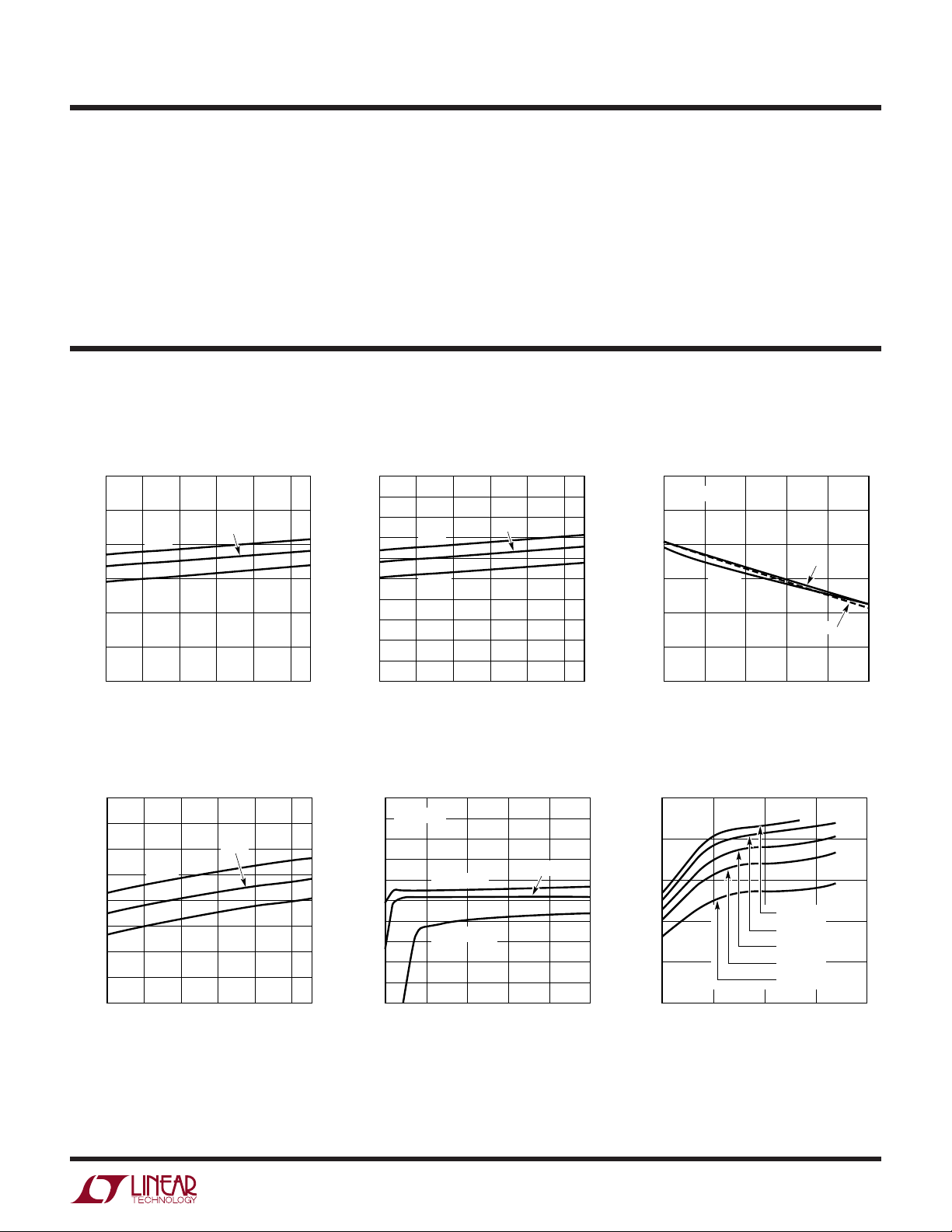
TYPICAL PERFOR A CE CHARACTERISTICS
No Load Supply Current vs Supply
Voltage (One Output Enabled)
60
50
40
30
(µA)
IN
I
20
10
0
2.7
85°C
–45°C
3.7 4.2 4.7
3.2
25°C
VIN (V)
5.2
3252 G01
No Load Supply Current vs Supply
Voltage (Both Outputs Enabled)
100
90
80
70
60
(µA)
50
CC
I
40
30
20
10
0
2.7
85°C
–40°C
3.7 4.2 4.7
3.2
25°C
VIN (V)
OUT(MIN)
5.2
3252 G02
+ ROL • I
0.82
0.81
0.80
(V)
0.79
FB
V
0.78
0.77
0.76
)
OUT
= (VIN/2 – V
OL
OUT
)/I
OUT
.
FB Voltage vs Load Current
VIN = 3.6V
25°C
–40°C
85°C
50 100 150 200 250
0
I
(mA)
OUT
3252 G03
EN1/EN2 Input Threshold Voltage
vs Supply Voltage
1.2
1.1
25°C
VIN (V)
(V)
SHDN
V
1.0
0.9
0.8
0.7
0.6
0.5
0.4
2.7
–40°C
85°C
3.7 4.2 4.7
3.2
5.2
3252 G04
1.5V Output Voltage vs Supply
Voltage
1.60
TA = 25°C
1.58
1.56
1.54
I
(V)
OUT
V
1.52
1.50
1.48
1.46
1.44
1.42
1.40
3
= 0mA
OUT
I
= 250mA
OUT
3.5 4 4.5 5 5.5
VIN (V)
I
OUT
= 50mA
3252 G05
1.5V Output Efficiency vs Output
Current
100
= 25°C
T
A
80
60
I
OUT
VIN = 3.1V
V
V
V
V
(mA)
= 3.3V
IN
= 3.6V
IN
= 4V
IN
= 5V
IN
40
EFFICIENCY (%)
20
0
0.1
1 10 100 1000
3252 G06
3252f
3
Page 4
LTC3252
UW
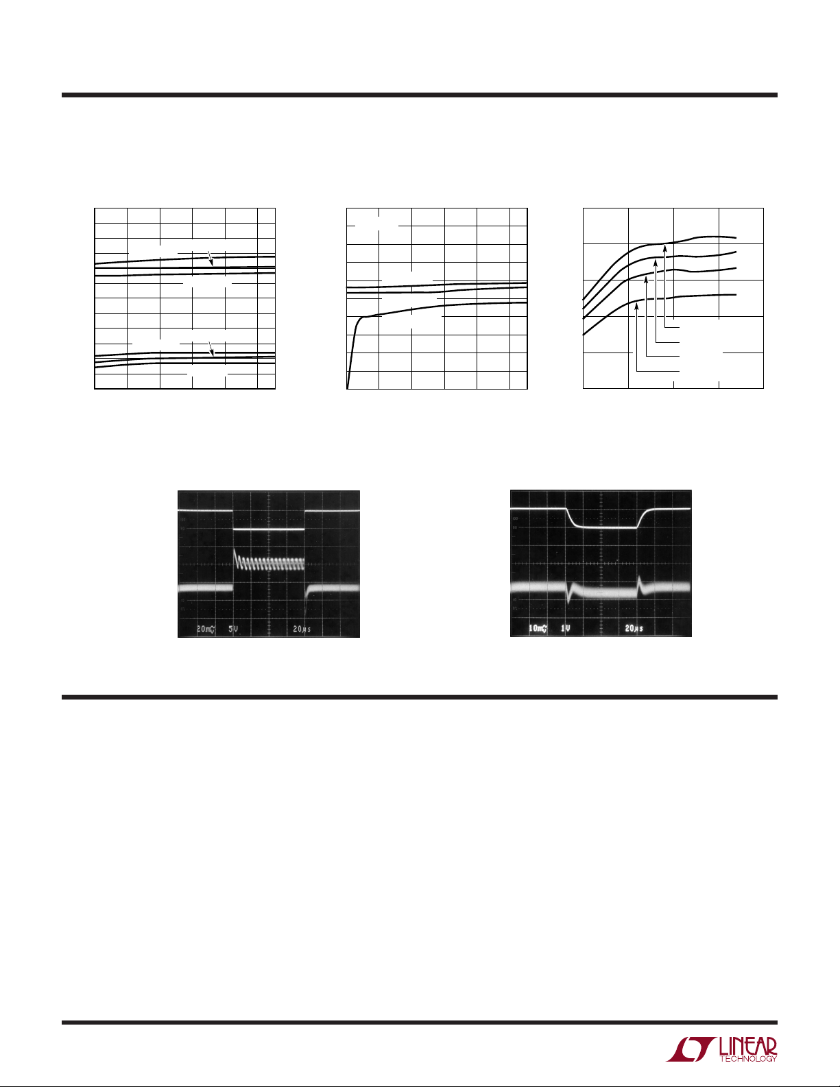
TYPICAL PERFOR A CE CHARACTERISTICS
Oscillator Max/Min Frequency vs
Supply Voltage
2.0
1.9
1.8
1.7
1.6
1.5
1.4
1.3
1.2
FREQUENCY (MHz)
1.1
1.0
0.9
0.8
2.7
–40°C MAX
3.2
–40°C MIN
25°C MAX
85°C MAX
25°C MIN
85°C MIN
3.7 4.2 4.7
VIN (V)
Output Current Transient
Response
250mA
I
OUT
20mA
V
OUT
20mV/DIV
AC
5.2
3252 G07
1.2V Output Voltage vs Supply
Voltage 1.2V Efficiency vs Load Current
100
TA = 25°C
80
60
40
EFFICIENCY (%)
20
0
0.1
VIN = 2.8V
V
V
V
1 10 100 1000
I
(mA)
OUT
(V)
OUT
V
1.30
1.28
1.26
1.24
1.22
1.20
1.18
1.16
1.14
1.12
1.10
2.7
TA = 25°C
3.2
I
= 0mA
OUT
I
= 50mA
OUT
I
= 250mA
OUT
3.7 4.2 4.7
VIN (V)
5.2
3252 G08
Line Transient Response
4.5V
V
IN
3.5V
V
OUT
10mV/DIV
AC
= 3.1V
IN
= 3.5V
IN
= 4.5V
IN
3252 G09
VIN = 3.6V
V
= 1.5V
OUT
3252 G11
UUU
PI FU CTIO S
FB1 (Pin 1): Feedback Input Pin 1. An output divider
should be connected from OUT1 to FB1 to program the
output voltage.
EN1 (Pin 2): Input Enable Pin 1. When EN1 is high, OUT1
is enabled. When EN1 is low OUT1 is shut down.
VIN (Pin 3): Input Supply Voltage. Operating VIN may be
between 2.7V and 5.5V. Bypass VIN with a ≥ 4.7µF (1µF
min) low ESR ceramic capacitor to GND (CIN).
V
I
OUT
OUT
= 1.5V
= 150mA
3252 G12
C1+ (Pin 4): Flying Capacitor 1 Positive Terminal (C1).
OUT1 (Pin 5): Regulated Output Voltage 1. OUT1 is
disconnected from VIN when in shutdown. Bypass OUT1
with a low ESR ceramic capacitor to GND (CO1). See
Output Capacitor Selection section for size requirements.
C1– (Pin 6): Flying Capacitor 1 Negative Terminal (C1).
GND (Pin 7): Ground. Connect to a ground plane for best
performance.
3252f
4
Page 5
UUU
PI FU CTIO S
LTC3252
C2– (Pin 8): Flying Capacitor 2 Negative Terminal (C2).
OUT2 (Pin 9): Regulated Output Voltage 2. OUT2 is
disconnected from VIN when in shutdown. Bypass OUT2
with a low ESR ceramic capacitor to GND (CO2). See
Output Capacitor Selection section for size requirements.
C2+ (Pin 10): Flying Capacitor 2 Positive Terminal (C2).
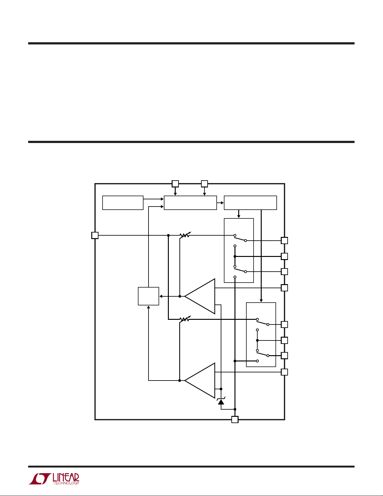
WW
SI PLIFIED
BLOCK DIGRAM
OVERTEMPERATURE
3V
IN
EN1
2
SWITCH
CONTROL
EN2 (Pin 11): Input Enable Pin 2. When EN2 is high, OUT2
is enabled. When EN2 is low OUT2 is shut down.
FB2 (Pin 12): Feedback Input Pin 2. An output divider
should be connected from OUT2 to FB2 to program the
output voltage.
EN2
11
SPREAD SPECTRUM
OSCILLATOR
CHARGE
PUMP 1
+
4
C1
BURST
DETECT
CIRCUIT
5
OUT1
–
6
C1
–
+
CHARGE
PUMP 2
–
1 FB1
C2
10
9
OUT2
8
C2
12 FB2
+
–
+
7
GND
3252 SBD
3252f
5
Page 6

LTC3252
OPERATIO
U
(Refer to Simplified Block Diagram)
The LTC3252 has two switched capacitor charge pumps to
step down VIN to two regulated output voltages. The two
charge pumps operate 180° out of phase to reduce input
ripple. Regulation is achieved by sensing each output
voltage through an external resistor divider and modulating the charge pump output current based on the error
signal. A 2-phase nonoverlapping clock activates the two
charge pumps running them out of phase from each other.
On the first phase of the clock current is transferred from
VIN, through the external flying capacitor 1, to OUT1 via the
switches of charge pump 1. Not only is current being
delivered to OUT1 on the first phase, but the flying capacitor is also being charged up. On the second phase of the
clock, flying capacitor 1 is connected from OUT1 to
ground, transferring the charge stored during the first
phase of the clock to OUT1 via the switches of charge
pump 1. Charge pump 2 operates in the same manner to
supply current to OUT2, but with the phases of the clock
reversed relative to charge pump 1. Using this method of
switching, only half of the output current for each output
is delivered from VIN, thus achieving a 50% increase in
efficiency over a conventional LDO. A spread spectrum
oscillator, which utilizes random switching frequencies
between 1MHz and 1.6MHz, sets the rate of charging and
discharging of the flying capacitors. This architecture
achieves extremely low output noise. Input noise is significantly reduced compared to conventional charge pumps.
The outputs also have a low current burst mode to improve
efficiency even at light loads.
In shutdown mode all circuitry is turned off and the
LTC3252 draws only leakage current from the VIN supply.
Furthermore, OUT1 and OUT2 are disconnected from VIN.
The EN1 and EN2 pins are CMOS inputs with threshold
voltages of approximately 0.8V to allow regulator control
with low voltage logic levels. The LTC3252 is in shutdown
when a logic low is applied to both enable pins. Since the
mode pins are high impedance CMOS inputs, they should
never be allowed to float. Always drive the enable pins with
valid logic levels.
Short-Circuit/Thermal Protection
The LTC3252 has built-in short-circuit current limiting as
well as over temperature protection. During short-circuit
conditions, internal circuitry automatically limits each
output to approximately 500mA of current. If fault conditions (such as shorted outputs) cause excessive self
heating on chip such that the junction temperature exceeds approximately 160°C, the thermal shutdown circuitry will disable the charge pumps. The IC resumes
operation once the junction temperature drops back to
approximately 155°C. The LTC3252 will cycle in and out of
thermal shutdown without latchup or damage until the
overstress condition is removed. Long term overstress
(I
or I
OUT1
avoided as it can degrade the performance or shorten the
life of the part.
Soft-Start
To prevent excessive current flow at VIN during start-up,
the LTC3252 has built-in soft-start circuitry on each output. When an output is enabled, the soft-start circuitry
increases the amount of current available from the output
linearly over a period of approximately 500µs. The soft-
start circuitry is disabled shortly after the output achieves
regulation.
Spread Spectrum Operation
Switching regulators can be particularly troublesome where
electromagnetic interference (EMI) is concerned. Switching regulators operate on a cycle-by-cycle basis to transfer
power to an output. In most cases, the frequency of
operation is either fixed or is a constant based on the
output load. This method of conversion creates large
components of noise at the frequency of operation (fundamental) and multiples of the operating frequency (harmonics).
> 400mA, and/or TJ > 125°C) should be
OUT2
6
3252f
Page 7
OPERATIO
LTC3252
U
(Refer to Simplified Block Diagram)
Unlike conventional buck converters, the LTC3252’s internal oscillator is designed to produce a clock pulse whose
period is random on a cycle-by-cycle basis but fixed
between 1MHz and 1.6MHz. This has the benefit of spreading the switching noise over a range of frequencies, thus
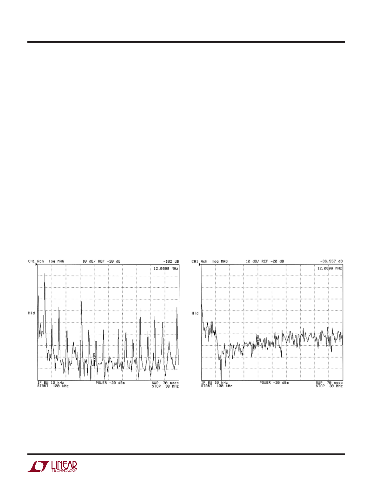
significantly reducing the peak noise. Figures 1 and 2
show how the spread spectrum feature of the LTC3252
significantly reduces the peak harmonic noise and virtually elliminates harmonics compared to a conventional
buck converter.
Spread spectrum operation is always enabled but is most
effective when the LTC3252’s outputs are out of Burst
Mode operation and the oscillator is running continuously
(see the Low Current Burst Mode Operation section).
Low Current Burst Mode Operation
To improve efficiency at low output currents, a Burst Mode
operation function is included in the LTC3252. An output
current sense is used to detect when the required output
current of both outputs drop below an internally set
threshold (30mA typ). When this occurs, the part shuts
down the internal oscillator and goes into a low current
operating state. The LTC3252 will remain in the low
current operating state until either output has dropped
enough to require another burst of current. The LTC3252
resumes continuous operation when the load on one or
both outputs exceeds the internally set threshold. Unlike
traditional charge pumps where the burst current is highly
dependant on many factors (i.e., supply, switch strength,
capacitor selection, etc.), the LTC3252’s burst current is
set by the burst threshold and hysteresis. This means that
the output ripple voltage in Burst Mode operation is
relatively consistent and is typically about 12mV with a
4.7µF output capacitor on a 1.5V output. The ripple voltage
amplitude is a direct function of the output capacitor size.
Burst Mode operation ripple voltage does increase slightly
at lower output voltages due to the increase in loop gain.
Users can counteract output voltage ripple increase through
the use of a slightly larger output capacitor. See Recommended Output Capacitance guidelines of Figure 3.
Figure 1. Conventional Buck Input Noise Figure 2. LTC3252 Input Noise
3252f
7
Page 8
LTC3252
OPERATIO
U
(Refer to Simplified Block Diagram)
Output Capacitor Selection
The style and value of capacitors used with the LTC3252
determine several important parameters such as regulator
control loop stability, output ripple and charge pump
strength.
The switching nature of the LTC3252 minimizes output
noise significantly but not completely. What small ripple
that exists at an output is controlled by the value of output
capacitor directly. Increasing the size of the output capacitor will proportionately reduce the output ripple. The ESR
(equivalent series resistance) of the output capacitor plays
the dominant role in output noise. When the LTC3252
switches between clock phases there is a period where all
switches are turned off. This “blanking period” shows up
as a spike at the output and is a direct function of the output
current times the ESR value. To reduce output noise and
ripple, it is suggested that a low ESR (<0.08Ω) ceramic
capacitor be used for the output capacitor. Tantalum and
aluminum capacitors are not recommended because of
their high ESR.
Both the style and value of the output capacitors can
significantly affect the stability of the LTC3252. As shown
in the Simplified Block Diagram, the LTC3252 uses a
control loop to adjust the strength of each charge pump to
match the current required at the output. The error signal
of each loop is stored directly on each output capacitor.
Thus the output capacitors also serve to form the dominant pole in each control loop. Figure 3 is a graph of the
recommended output capacitance, and minimum capaci-
8
tance required for good transient response (see the Ceramic Capacitor Selection Guidelines section).
Likewise excessive ESR on the output capacitor will tend
to degrade the loop stability of the LTC3252. The closed
loop output impedance of the LTC3252 is approximately:
V
R
=Ω00808.•
O
For example, with the output programmed to 1.5V, the R
OUT
.
V
O
is 0.15Ω, which produces a 38mV output change for a
250mA load current step. For stability and good load
transient response it is important for the output capacitor
to have 0.1Ω or less of ESR. Ceramic capacitors typically
have exceptional ESR and combined with a tight board
layout should yield excellent stability and load transient
performance.
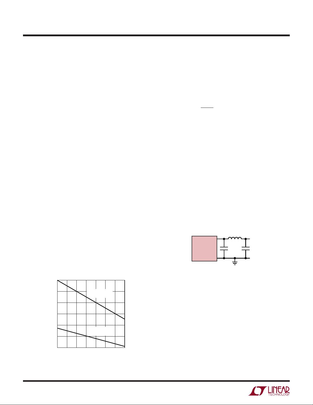
Further output noise reduction can be achieved by filtering
the LTC3252 outputs through a very small series inductor
as shown in Figure 4. A 10nH inductor will reject the fast
output transients caused by the blanking period, thereby
presenting a nearly constant output voltage. For economy
the 10nH inductor can be fabricated on the PC board with
about 1cm (0.4") of PC board trace.
OUT
LTC3252
GND
Figure 4. 10nH Inductor Used for
Additional Output Noise Reduction
10nH
4.7µF 0.47µF
V
3252 F04
OUT
8
7
6
(µF)
5
OUT
C
4
3
2
1 1.1 1.2 1.3 1.4 1.5 1.6
0.9
Figure 3. Output Capacitance vs Output Voltage
RECOMMENDED
CAPACITANCE
MINIMUM
CAPACITANCE
V
(V)
OUT
3252 F03
VIN Capacitor Selection
The low noise, dual phase architecture used by the LTC3252
makes input noise filtering much less demanding than
conventional charge pump regulators. The LTC3252 input
current will transition between I
OUT1
/2 and I
OUT2
/2 for
each half cycle of the oscillator. The blanking period
described in the V
section also effects the input. For
OUT
this reason it is recommended that a low ESR 4.7µF (1µF
min) or greater ceramic capacitor be used for CIN (see the
Ceramic Capacitor Selection Guidelines section). Aluminum and tantalum capacitors can be used but are not
recommended because of their high ESR.
3252f
Page 9
OPERATIO
LTC3252
U
(Refer to Simplified Block Diagram)
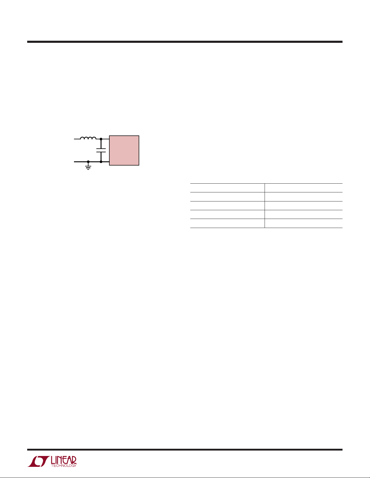
Further input noise reduction can be achieved by filtering
the input through a very small series inductor as shown in
Figure 5. A 10nH inductor will reject the fast input transients caused by the blanking period, thereby presenting
a nearly constant load to the input supply. For economy the
10nH inductor can be fabricated on the PC board with
about 1cm (0.4") of PC board trace.
10nH
V
IN
SUPPLY
4.7µF
Figure 5. 10nH Inductor Used for
Additional Input Noise Reduction
V
IN
GND
LTC3252
3252 F05
Flying Capacitor Selection
Warning: A polarized capacitor such as tantalum or aluminum should never be used for the flying capacitors since
their voltages can reverse upon start-up of the LTC3252.
Ceramic capacitors should always be used for the flying
capacitors.
The flying capacitors control the strength of the charge
pump. In order to achieve the rated output current it is
necessary for the flying capacitor to have at least 0.4µF of
capacitance over operating temperature with a 2V bias
(see the Ceramic Capacitor Selection Guidelines). If 100mA
or less of current is required from an output then its associated flying capacitor minimum can be reduced to 0.15µF.
discussing the specified capacitance value. For example,
over rated voltage and temperature conditions, a 4.7µF,
10V, Y5V ceramic capacitor in a 0805 case may not
provide any more capacitance than a 1µF, 10V, X7R
available in the same 0805 case. In fact, over bias and
temperature range, the 1µF, 10V, X7R will provide more
capacitance than the 4.7µF, 10V, Y5V. The capacitor
manufacturer’s data sheet should be consulted to determine what value of capacitor is needed to ensure minimum capacitance values are met over operating
temperature and bias voltage.
Below is a list of ceramic capacitor manufacturers and
how to contact them:
AVX www.avxcorp.com
Kemet www.kemet.com
Murata www.murata.com
Taiyo Yuden www.t-yuden.com
Vishay www.vishay.com
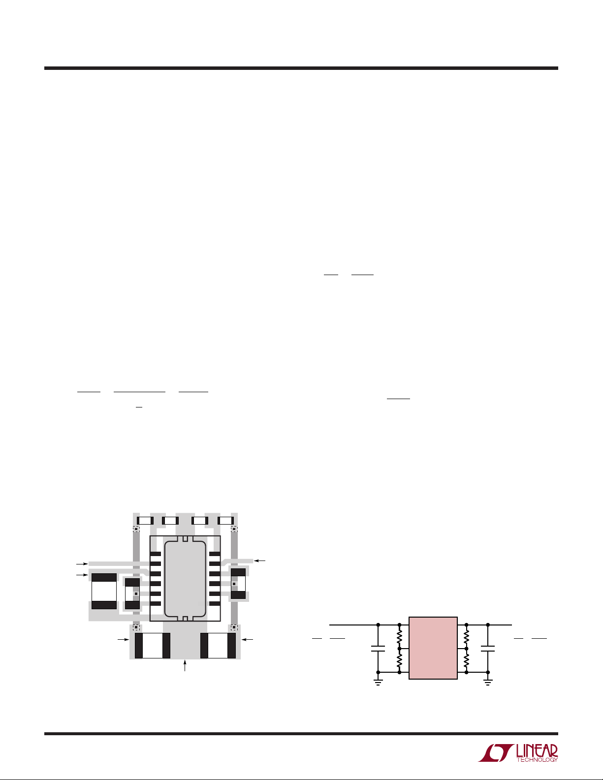
Layout Considerations
Due to the high switching frequency and transient currents
produced by the LTC3252 careful board layout is necessary for optimal performance. A true ground plane and
short connections to all capacitors will improve performance and ensure proper regulation under all conditions.
Figure 7 shows the suggested layout configuration. Note
the exposed paddle of the package is ground (GND) and
must be soldered to the PCB ground.
Ceramic Capacitor Selection Guidelines
Capacitors of different materials lose their capacitance
with higher temperature and voltage at different rates. For
example, a ceramic capacitor made of X7R material will
retain most of its capacitance from – 40°C to 85°C whereas
a Z5U or Y5V style capacitor will lose considerable
capacitance over that range (60% to 80% loss typical).
Z5U and Y5V capacitors may also have a very strong
voltage coefficient causing them to lose an additional
60% or more of their capacitance when the rated voltage
is applied. Therefore, when comparing different capacitors it is often more appropriate to compare the amount
of achievable capacitance for a given case size rather than
The flying capacitor pins C1+, C1–, C2+ and C2– will have
very high edge rate wave forms. The large dv/dt on these
pins can couple energy capacitively to adjacent printed
circuit board runs. Magnetic fields can also be generated
if the flying capacitors are not close to the LTC3252 (i.e.,
the loop area is large). To decouple capacitive energy
transfer, a Faraday shield may be used. This is a grounded
PC trace between the sensitive node and the LTC3252
pins. For a high quality AC ground, it should be returned to
a solid ground plane that extends all the way to the
LTC3252. Keep the FB traces away from or shielded from
the flying capacitor traces or degraded performance could
result.
3252f
9
Page 10
LTC3252
OPERATIO
U
(Refer to Simplified Block Diagram)
Thermal Management
To reduce the maximum junction temperature, a good
thermal connection to the PC board is recommended.
Soldering the exposed paddle of the IC to the PCB and
maintaining a solid ground plane under the device on one
or more layers of the PC board, the thermal resistance of
the package can be as small as 40°C/W. By applying the
suggested thermal management techniques the IC junction temperature should never exceed 125°C even under
worst case operating conditions.
Power Efficiency
The power efficiency (η) of the LTC3252 is approximately
50% higher than a conventional linear regulator. This
occurs because the input current for a 2-to-1 step-down
charge pump is approximately half the output current. For
an ideal 2-to-1 step-down charge pump the power efficiency is given by:
P
OUT
η≡ = =
P
IN
VI
•
OUT OUT
1
VI
•
IN OUT
2
V
2
OUT
V
IN
The switching losses and quiescent current of the LTC3252
are designed to minimize efficiency loss over the entire
output current range, causing only a couple % error from
the theoretical efficiency. For example with VIN = 3.6V,
R
R
B
LTC3252
RB' RA'
EN2
C2
EN1
V
A
1
IN
C
IN
C1
I
= 150mA and OUT1 regulating at 1.5V the measured
OUT1
efficiency is 80.6% which is in close agreement with the
theoretical 83.3% calculation.
Programming the LTC3252 Output Voltages (FB1 and
FB2 Pin)
Each output of the LTC3252 is programmed to an arbitrary
voltage via an external resistive divider. Figure 7 shows the
required voltage divider connection. The voltage divider
ratio is given by the expression:
R
OUT
A
=−
R
B
081.
V
Typical values for total voltage divider resistance can
range from several kΩs up to 1MΩ.
The user may want to consider load regulation when
setting the desired output voltage. The closed loop output
impedance of the LTC3252 is approximately:
R
=Ω00808.•
O
OUT
.
V
For a 1.5V output, RO is 0.15Ω, which produces a 38mV
output change for a 250mA load current step. Thus, the
user may want to target an unloaded output voltage
slightly higher than desired to compensate for the output
load conditions. The output may be programmed for
regulation voltages of 0.9V to 1.6V.
Since the LTC3252 employs a 2-to-1 charge pump architecture, it is not possible to achieve output voltages
greater than half the available input voltage. The minimum
VIN supply required for regulation can be determined by
the following equation:
VIN (MIN) ≤ 2 • (V
(MIN) + I
OUT
OUT
• ROL)
10
C
O1
(CONNECT DIRECTLY TO GROUND PLANE)
GND
C
O2
Figure 6. Suggested Layout for the LTC3252
OUT1
OUT1
R
A
OUT2OUT1
3252 F06
=– 1
R
0.8V
B
C
O1
OUT1
R
A
FB1
R
B
GND
LTC3252
OUT2
FB2
GND
RA'
RB'
C
O2
OUT2
'
OUT2
R
A
=– 1
'
R
0.8V
B
3252 F07
Figure 7. Programming the LTC3252
3252f
Page 11
TYPICAL APPLICATIO
OUT1
1.2V
250mA
4.7µF
Li-ION
4.7µF
PACKAGE DESCRIPTIO
U
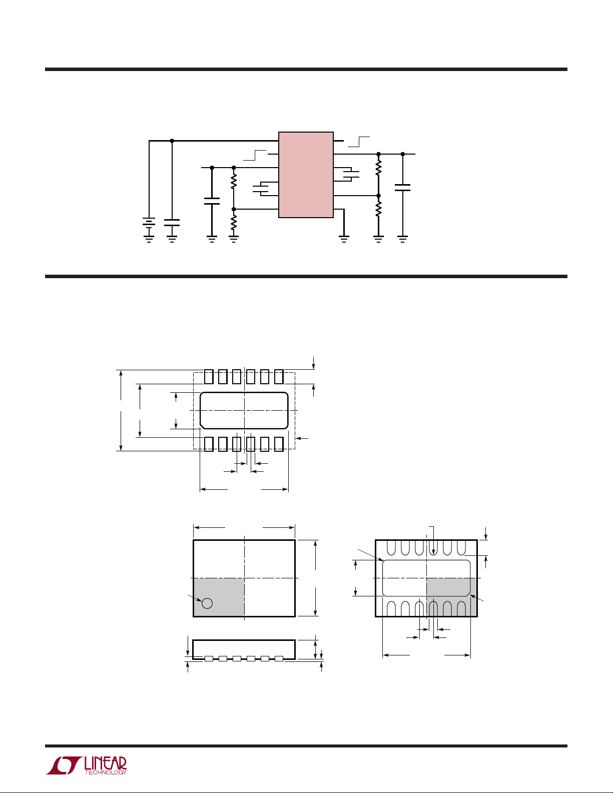
Li-Ion to 1.5V/1.2V Outputs
261k
OFF ON
1µF
510k
V
IN
EN1
OUT1
C1
C1
FB1
LTC3252
+
–
EN2
OUT2
C2
C2
FB2
GND
U
DE/UE Package
12-Lead Plastic DFN (4mm × 3mm)
(Reference LTC DWG # 05-08-1695)
LTC3252
113
OFF ON
92
105
+
84
–
126
71
1µF
470k
510k
4.7µF
3252 TA02
OUT2
1.5V
250mA
3.40 ±0.05
0.58 ±0.05
1.70 ±0.05
(2 SIDES)2.24 ±0.05
PACKAGE OUTLINE
0.25 ± 0.05
3.30 ±0.05
(2 SIDES)
RECOMMENDED SOLDER PAD PITCH AND DIMENSIONS
4.00 ±0.10
(2 SIDES)
PIN 1
TOP MARK
0.200 REF
NOTE:
1. DRAWING PROPOSED TO BE A VARIATION OF VERSION
(WGED) IN JEDEC PACKAGE OUTLINE M0-229
2. ALL DIMENSIONS ARE IN MILLIMETERS
3. DIMENSIONS OF EXPOSED PAD ON BOTTOM OF PACKAGE DO NOT INCLUDE
MOLD FLASH. MOLD FLASH, IF PRESENT, SHALL NOT EXCEED 0.15mm ON ANY SIDE
4. EXPOSED PAD SHALL BE SOLDER PLATED
0.50
BSC
3.00 ±0.10
(2 SIDES)
0.75 ±0.05
R = 0.20
TYP
1.70 ± 0.10
(2 SIDES)
0.00 – 0.05
R = 0.115
TYP
0.25 ± 0.05
3.30 ±0.10
(2 SIDES)
BOTTOM VIEW—EXPOSED PAD
0.50
BSC
127
16
0.38 ± 0.10
PIN 1
NOTCH
(UE12/DE12) DFN 0802
3252f
Information furnished by Linear Technology Corporation is believed to be accurate and reliable.
However, no responsibility is assumed for its use. Linear Technology Corporation makes no representation that the interconnection of its circuits as described herein will not infringe on existing patent rights.
11
Page 12
LTC3252
TYPICAL APPLICATIO S
U
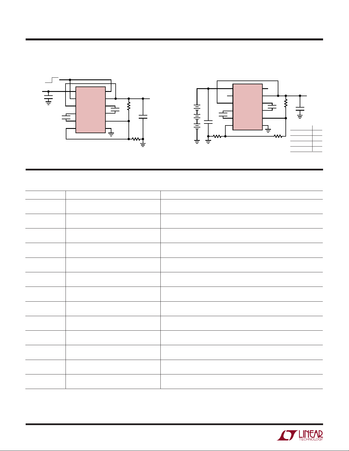
3-Cell NiMH with Digitally Selectable 1.2V/1.5V Output
V
IN
EN1EN1
OUT1
LTC3252
+
3-CELL
NiMH
1µF
4.7µF
412k 100k
C1
C1
FB1
–
3.3V
Fixed 3.3VIN to 1.5V
OFF ON
4.7µF
1µF
V
IN
EN1
OUT1
C1
C1
FB1
LTC3252
+
–
OUT
EN2
OUT2
C2
C2
FB2
GND
at 300mA
113
92
105
+
84
–
126
71
1µF
470k
510k
10µF
3252 TA03
OUT
1.5V
300mA
RELATED PARTS
PART NUMBER DESCRIPTION COMMENTS
LTC1514 50mA, 650kHz, Step-Up/Down Charge Pump VIN = 2.7V to 10V, V
with Low Battery Comparator I
SHDN
= 10µA, S8
LTC1515 50mA, 650kHz, Step-Up/Down Charge Pump VIN = 2.7V to 10V, V
with Power-On Reset I
LT1776 500mA (I
Step-Down DC/DC Converter I
), 200kHz, High Efficiency 90% Efficiency, VIN = 7.4V to 40V, V
OUT
= <1µA, S8
SHDN
= 3.2mA, I
Q
SHDN
LTC1911-1.5 250mA, 1.5MHz, High Efficiency 75% Efficiency, VIN = 2.7V to 5.5V, V
Step-Down Charge Pump I
= 180µA, I
Q
SHDN
LTC1911-1.8 250mA, 1.5MHz, High Efficiency 75% Efficiency, VIN = 2.7V to 5.5V, V
Step-Down Charge Pump I
= 180µA, I
Q
SHDN
LTC3250-1.5 250mA, 1.5MHz, High Efficiency 85% Efficiency, VIN = 3.1V to 5.5V, V
Step-Down Charge Pump I
= 35µA, I
Q
SHDN
LTC3251 500mA, Spread Spectrum, High Efficiency Up to 85% Efficiency, VIN = 2.7V to 5.5V, V
Step-Down Charge Pump I
LTC3404 600mA (I
Step-Down DC/DC Converter I
LTC3405/LTC3405A 300mA (I
Step-Down DC/DC Converter I
LTC3406/LTC3406B 600mA (I
Step-Down DC/DC Converter I
LTC3411 1.25A (I
DC/DC Converter I
LTC3412 2.5A (I
OUT
DC/DC Converter I
LTC3440 600mA (I
Buck-Boost DC/DC Converter I
), 1.4MHz, Synchronous 95% Efficiency, VIN = 2.7V to 6V, V
OUT
), 1.5MHz, Synchronous 95% Efficiency, VIN = 2.7V to 6V, V
OUT
), 1.5MHz, Synchronous 95% Efficiency, VIN = 2.5V to 5.5V, V
OUT
), 4MHz, Synchronous Step-Down 95% Efficiency, VIN = 2.5V to 5.5V, V
OUT
), 4MHz, Synchronous Step-Down 95% Efficiency, VIN = 2.5V to 5.5V, V
), 2MHz, Synchronous 95% Efficiency, VIN = 2.5V to 5.5V, V
OUT
= 8µA, I
Q
= 10µA, I
Q
= 20µA, I
Q
= 20µA, I
Q
= 60µA, I
Q
= 60µA, I
Q
= <25µA, I
Q
SHDN
SHDN
SHDN
SHDN
SHDN
SHDN
SHDN
= 3V or 5V, Regulated Output, IQ = 60µA,
OUT
= 3.3V or 5V, Regulated Output, IQ = 60µA,
OUT
Min = 1.24V,
OUT
= 30µA, N8, S8
= 1.5V, Regulated Output,
OUT
= 10µA, MS8
= 1.8V, Regulated Output,
OUT
= 10µA, MS8
= 1.5V, Regulated Output,
OUT
= <1µA, ThinSOT
= <1µA, MS10
Min = 0.8V,
OUT
= <1µA, MS8
Min = 0.8V,
OUT
= <1µA, ThinSOT
Min = 0.6V,
OUT
= <1µA, ThinSOT
Min = 0.8V,
OUT
= <1µA, MS10
Min = 0.8V,
OUT
= <1µA, TSSOP-16E
Min = 2.5V,
OUT
= 1µA, MS10
113
EN2 EN2
92
OUT2
105
+
C2
84
–
C2
126
FB2
71
GND
= 0.9V to 1.6V,
OUT
1µF
I
OUT
261k
250mA
4.7µF
EN1 EN2 OUT
OFF OFF 0V
OFF ON 1.2V
ON OFF 1.5V
ON ON 1.5V
3252 TA04
12
Linear Technology Corporation
1630 McCarthy Blvd., Milpitas, CA 95035-7417
(408) 432-1900 ● FAX: (408) 434-0507
●
www.linear.com
3252f
LT/TP 0503 1K • PRINTED IN USA
LINEAR TECHNOLOGY CORPORATION 2003
 Loading...