

Compact I2C-Controllable Quad Synchronous Step-Down
DC/DC Regulator for Power-Conscious Portable Processors
Design Note 442
Jim Drew
Introduction
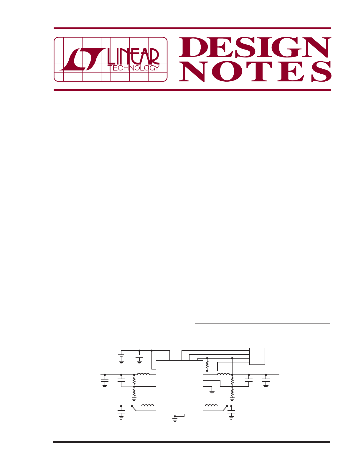
The LTC®3562 quad output step-down regulator is designed
for multicore handheld microprocessor applications that
operate from a single Li-Ion bat tery. Its four monolithic, high
effi cienc y buck regulators suppor t Intel’s mobile CPU P-State
and C-State energy saving operating modes. The output
2
voltages are independently controllable via I
C, and each
output can be indep endently star ted and shut down. Designers can choose from power saving pulse-skipping mode or
Burst Mode
®
operation, or select low noise LDO mode. The
space-saving LTC3562 is available in a 3mm × 3mm QFN
package and requires few external components.
Four I2C-Controllable Regulators
Two of the regulators provide up to 600mA of output
current each while the other two provide up to 400mA
each. All regulators are internally compensated, so no
external compensation components are needed.
One of the 60 0mA regulators and one of t he 400mA regula-
2
tors (R600 A and R400A) feature I
C-controllable feedback
voltages, as shown in Figure 1. The output voltages of
these “Type A” regulators are set by a combination of ex-
2
ternal programming resistors and I
C-adjustable feedback
voltages—16 settings from 425mV to 800mV.
The “Type B” regula tors (R600B and R40 0B) do not require
extern al programming resistors bec ause the resistors are
integrated on-chip. The values of the internal feedback
2
resistors are adjusted through the I
C port, resulting in
128 possible output voltages from 600mV to 3.775V in
25mV increments.
Inrush current limiting is provided by soft-start circuitry
in all four regulators, as well as short-circuit protection
and switch node slew rate limiting to reduce EMI.
Power Saving Operating Modes
The LTC3562’s step-dow n regulators offer four sel ectable
modes of operation, which make it possible to balance
low noise against effi ciency. The four operating modes
of the LTC3562 are shown in Figure 2.
At moderate to heavy loads, the constant frequency
pulse-skipping mode provides the best output switching
noise solution. At lighter loads, ei ther Burst Mode operation
o r f o r c e d B u r s t M o d e o p e r a t i o n c a n b e s e l e c t e d t o m a x i m i z e
effi ciency, though these modes produce higher ripple.
If the application calls for the lowest possible noise,
LDO mode can be used for up to 50mA of load current.
L, LT, LTC, LTM, and Burst Mode are registered trademarks of Linear Technology
Corporation. All other trademarks are the property of their respective owners.
05/08/442
V
OUT
400A
1.5V
400mA
OUT
400B
1.2V
400mA
+
10pF10
μF
10
10
μF
SCL SDA DV
V
IN
RUN400A
SW400A
475k
536k
4.7μH
μF
LTC3562
FB400A
SW400B
OUT400B OUT600B
PGND AGND
POR600A
SW600A
FB600A
RUN600A
SW600B
3562 TA01
CC
100k
3.3
μH4.7μH
3.3μH
Li-Ion/Polymer
3.4V TO 4.2V
V
Figure 1. High Effi ciency Quad Step-Down Converter with I2C Control
MICROPROCESSOR
634k
499k
V
OUT
3.3V
600mA
μF
10
SDA
SCL
DV
POR
10pF
600B
CC
V
600A
OUT
1.8V
600mA
10μF
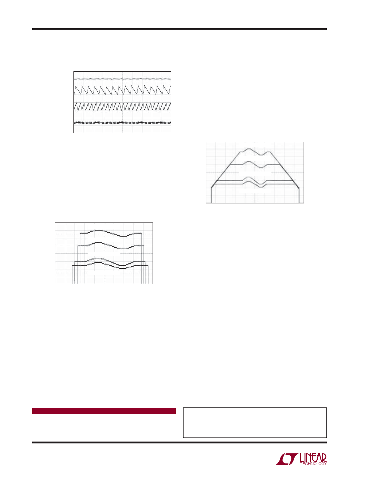
All four converters support 100% duty cycle operation
when the input voltage drops very close to the output
voltage setting.
OUT 400B = 3.3V
LDO Mode
OUT 600B = 2.5V
Forced Burst Mode
OUT 600A = 1.5V
Burst Mode
OUT 400A = 1.2V
Pulse Skip Mode
which ramps down with the fi rst. This is repeated until
each output has tracked down to a minimum value and
then disabled.
The ability to adjust the output voltage on the fl y is also
useful to margin the supplies for design evaluation or
manufacturing quality audit testing. Voltage margining
is applied to the nominal operating voltages in Figure 3
and Figure 4.
Reducing the voltage or shutting down any output can
reduce battery life or reduce energy usage in ‘green’
applications.
Figure 2. Modes of Operation
I2C Programming of Output Voltages Allows Easy
Sequencing, Tracking and Margining
Each output can be programmed on the fl y and independently enabled or disabled. These features taken together
enable almost any sequencing or tracking scheme. A
sequencing example is shown in Figure 3.
OUT 400B = 3.3V
OUT 600B = 2.5V
OUT 600A = 1.5V
OUT 400A = 1.2V
Figure 3. LTC3562 Voltage Sequencing and Margining
A coincident voltage tracking example is shown in Figure
4. All of the outputs are ramped up together at power up.
At power down, the highest out put is incrementally ramp ed
down until it reaches the value of the next higher voltage,
OUT 400B = 3.3V
OUT 600B = 2.5V
OUT 600A = 1.5V
OUT 400A = 1.2V
Figure 4. LTC3562 Voltage Tracking and Margining
Conclusion
The LTC3562 is a versatile high effi ciency quad output
monolithic synchronous buck regulator controlled with
2
C interface in a 3mm × 3mm QFN package. Four
an I
modes of operation allow the switching regulators to be
tailored to the system’s ef fi ciency and noise requirements.
This device is well suited for handheld microprocessor
applications operating from a single Li-Ion battery where
2
battery life is critical. The ability to use I
C to adjust
output voltages on the fl y or disable output voltages
supports Intel’s mobile CPU P-State and C-State energy
saving modes of operation and simplifi es development
and manufacturing tolerance testing.
Data Sheet Download
www.linear.com
Linear Technology Corporation
1630 McCarthy Blvd., Milpitas, CA 95035-7417
(408) 432-1900
●
FAX: (408) 434-0507 ● www.linear.com
For applications help,
call (978) 656-3768
dn442F LT/TP 0508 246K • PRINTED IN THE USA
© LINEAR TECHNOLOGY CORPORATION 2007
 Loading...