

LTC3559/LTC3559-1
Linear USB Battery Charger
with Dual Buck Regulators
FEATURES
Battery Charger
n
Standalone USB Charger
n
Up to 950mA Charge Current Programmable via
Single Resistor
n
HPWR Input Selects 20% or 100% of Programmed
Charge Current
n
NTC Input for Temperature Qualifi ed Charging
n
Internal Timer Termination
n
Bad Battery Detection
n
CHRG Indicates C/10 or Timeout
Buck Regulators
n
400mA Output Current
n
2.25MHz Constant Frequency Operation
n
Zero Current in Shutdown
n
Low Noise Pulse Skip Operation or Power Saving
Burst Mode Operation
n
Low No-Load Quiescent Current: 35μA
n
Available in a Low Profi le Thermally Enhanced
16-Lead 3mm × 3mm QFN Package
APPLICATIONS
DESCRIPTION
The LTC®3559/LTC3559-1 are USB battery chargers with
dual high effi ciency buck regulators. The parts are ideally
suited to power single-cell Li-Ion/Polymer based handheld
applications needing multiple supply rails.
Battery charge current is programmed via the PROG pin
and the HPWR pin, with capability up to 950mA at the BAT
pin. The battery charger has an NTC input for temperature
qualifi ed charging. The CHRG pin allows battery status to
be monitored continuously during the charging process.
An internal timer controls charger termination.
Each monolithic synchronous buck regulator provides up
to 400mA of output current while operating at effi ciencies
greater than 90% over the entire Li-Ion/Polymer range.
A MODE pin provides the fl exibility to place both buck
regulators in a power saving Burst Mode
low noise pulse skip mode.
The LTC3559/LTC3559-1 are offered in a low profi le thermally enhanced 16-lead (3mm × 3mm) QFN package.
L, LT, LTC and LTM are registered trademarks of Linear Technology Corporation.
All other trademarks are the property of their respective owners.
®
operation or a
n
SD/Flash-Based MP3 Players
n
Low Power Handheld Applications
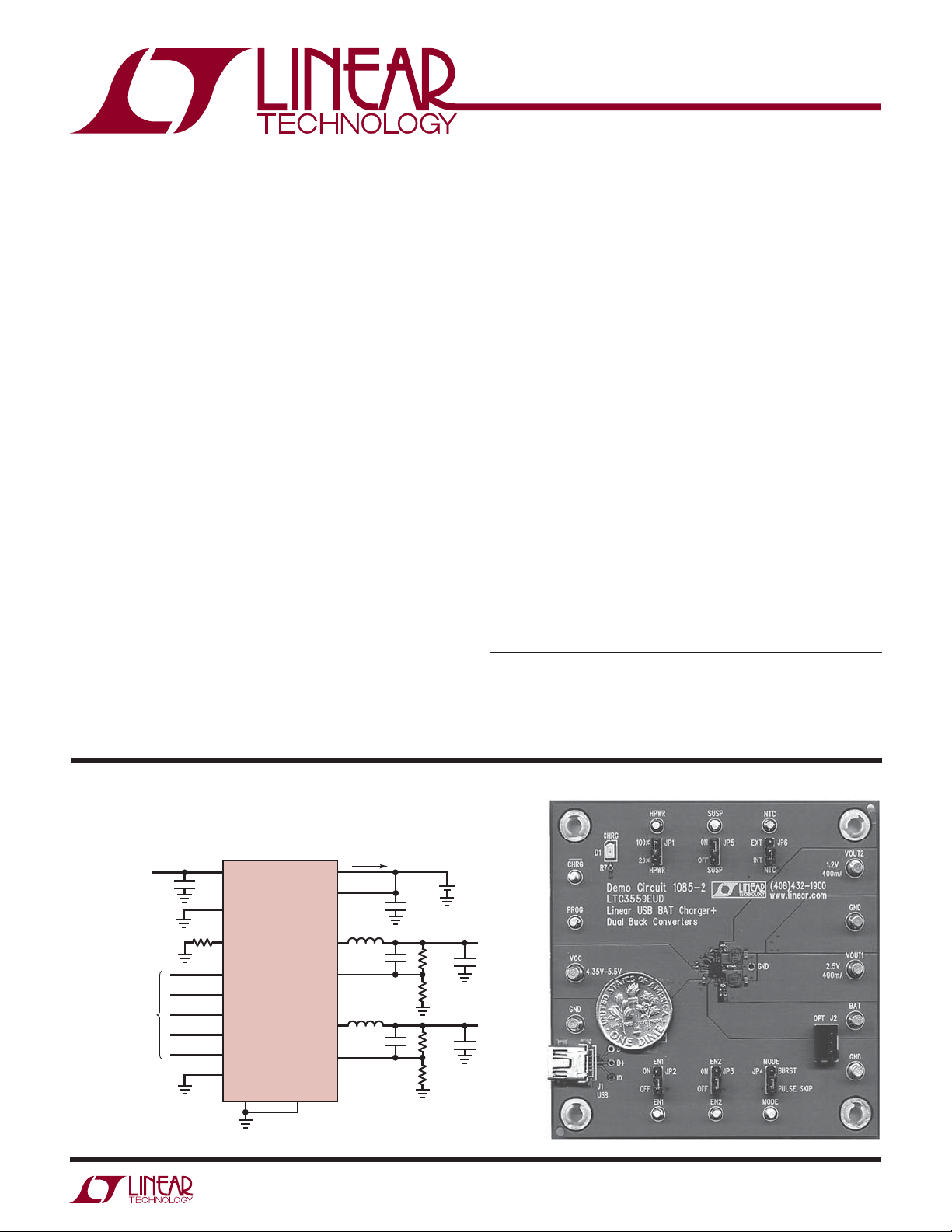
TYPICAL APPLICATION
USB Charger Plus Dual Buck Regulators
USB (4.3V TO 5.5V)
OR AC ADAPTOR
DIGITAL
CONTROL
1μF
1.74k
V
CC
NTC
PROG
CHRG
SUSP
HPWR
EN1
EN2
MODE
GND
LTC3559
EXPOSED
PAD
BAT
PV
SW1
FB1
SW2
FB2
IN
UP TO 500mA
4.7μH
22pF
4.7μH
22pF
2.2μF
+
655k
309k
324k
649k
3559 TA01
SINGLE
Li-lon CELL
(2.7V TO 4.2V)
2.5V
400mA
10μF
1.2V
400mA
10μF
3559fb
1
LTC3559/LTC3559-1
ABSOLUTE MAXIMUM RATINGS
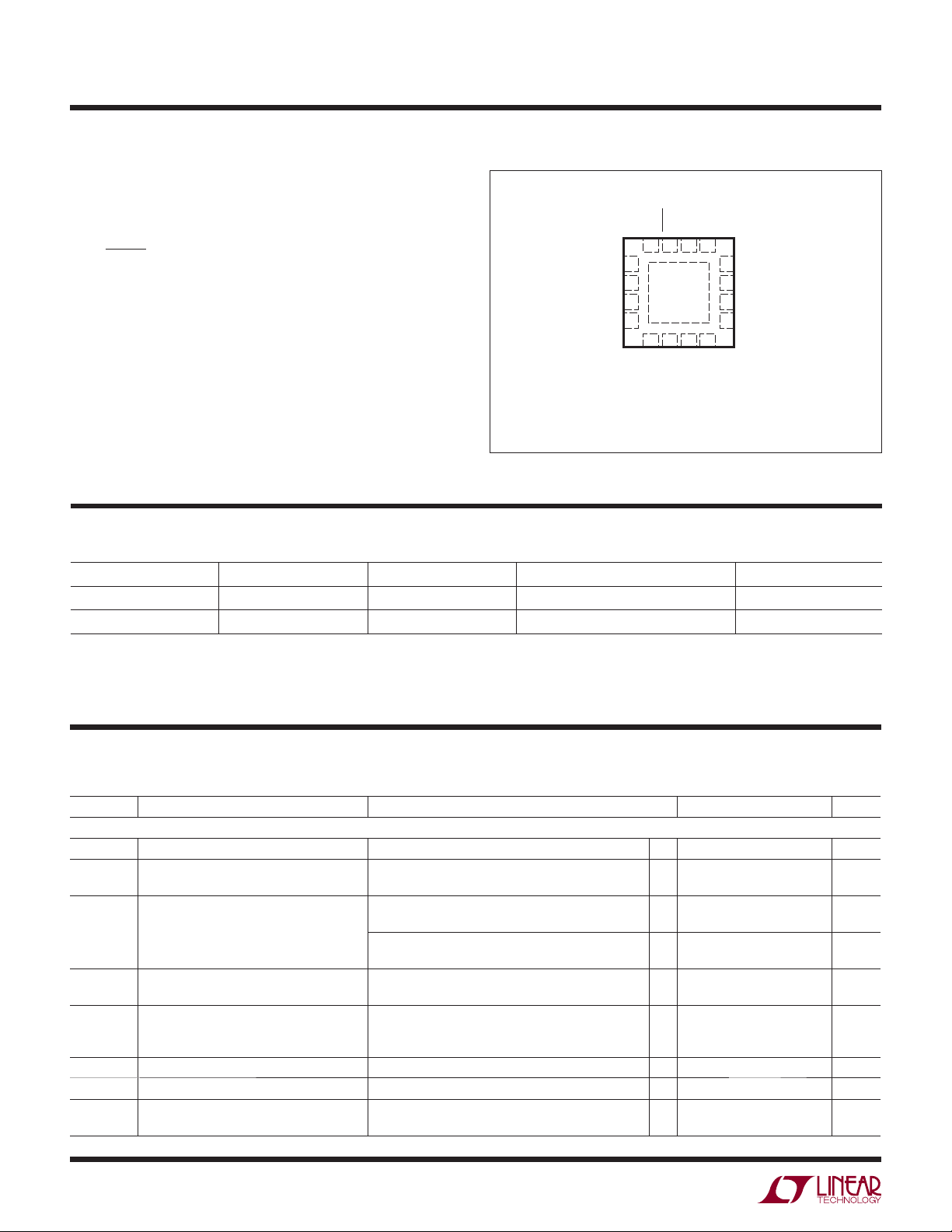
PIN CONFIGURATION
(Note 1)
VCC (Transient);
t < 1ms and Duty Cycle < 1% ....................... –0.3V to 7V
(Static) .................................................. –0.3V to 6V
V
CC
BAT, CHRG, SUSP ........................................ –0.3V to 6V
HPWR, NTC, PROG .......–0.3V to Max (V
, BAT) + 0.3V
CC
PROG Pin Current ...............................................1.25mA
BAT Pin Current ..........................................................1A
................................................–0.3V to BAT + 0.3V
PV
IN
EN1, EN2, MODE .......................................... –0.3V to 6V
FB1, FB2, SW1, SW2 ............–0.3V to PV
, I
I
SW1
......................................................600mA DC
SW2
+ 0.3V or 6V
IN
Junction Temperature (Note 2) ............................. 125°C
BAT
MODE
FB1
16-LEAD (3mm s 3mm) PLASTIC QFN
EXPOSED PAD (PIN 17) IS GND, MUST BE SOLDERED TO PCB
TOP VIEW
VCCCHRG
16 15 14 13
1GND
2
17
3
4
5 6 7 8
EN1
SW1
UD PACKAGE
T
= 125°C, θJA = 68°C/W
JMAX
PROG
IN
PV
NTC
SW2
12
HPWR
SUSP
11
FB2
10
EN2
9
Operating Temperature Range (Note 3).... –40°C to 85°C
Storage Temperature ..............................–65°C to 125°C
ORDER INFORMATION
LEAD FREE FINISH TAPE AND REEL PART MARKING PACKAGE DESCRIPTION TEMPERATURE RANGE
LTC3559EUD#PBF LTC3559EUD#TRPBF LCMB
LTC3559EUD-1#PBF LTC3559EUD-1#TRPBF LDQD
Consult LTC Marketing for parts specifi ed with wider operating temperature ranges.
Consult LTC Marketing for information on non-standard lead based fi nish parts.
For more information on lead free part marking, go to: http://www.linear.com/leadfree/
For more information on tape and reel specifi cations, go to: http://www.linear.com/tapeandreel/
16-Lead (3mm × 3mm) Plastic QFN
16-Lead (3mm × 3mm) Plastic QFN
–40°C to 85°C
–40°C to 85°C
The l denotes specifi cations that apply over the full operating temperature
ELECTRICAL CHARACTERISTICS
range, otherwise specifi cations are at TA = 25°C.
SYMBOL PARAMETER CONDITIONS MIN TYP MAX UNITS
Battery Charger. V
V
CC
I
VCC
V
FLOAT
I
CHG
I
BAT
V
UVLO
ΔV
V
DUVLO
UVLO
Input Supply Voltage
Battery Charger Quiescent Current (Note 4) Standby Mode, Charge Terminated
BAT Regulated Output Voltage LTC3559
Constant-Current Mode Charge Current HPWR = 5V
Battery Drain Current Standby Mode, Charger Terminated
Undervoltage Lockout Threshold BAT = 3.5V, VCC Rising 3.85 4.0 4.125 V
Undervoltage Lockout Hysteresis BAT = 3.5V 200 mV
Differential Undervoltage Lockout
Threshold
= 5V, BAT = PVIN = 3.6V, R
CC
= 1.74k, HPWR = 5V, SUSP = NTC = EN1 = EN2 = 0V
PROG
Suspend Mode, V
0°C ≤ T
≤ 85°C, LTC3559
A
LTC3559-1
≤ 85°C, LTC3559-1
0°C ≤ T
A
HPWR = 0V
Shutdown, V
Suspend Mode, SUSP = 5V, BAT = V
BAT = 4.05V, (VCC – BAT) Falling (LTC3559)
BAT = 3.95V, (V
CC
= 5V
SUSP
< V
, BAT = V
UVLO
– BAT) Falling (LTC3559-1)
CC
FLOAT
FLOAT
l
4.3 5.5 V
4.179
4.165
4.079
4.065
l
4408446092500
30
30
200
8.5
4.200
4.200
4.100
4.100
–3.5
–2.5
–1.5
50
50
400
17
4.221
4.235
4.121
4.135
100
–7
–4
–3
70
70
μA
μA
V
V
V
V
mA
mA
μA
μA
μA
mV
mV
3559fb
2
LTC3559/LTC3559-1
ELECTRICAL CHARACTERISTICS
The l denotes specifi cations that apply over the full operating temperature
range, otherwise specifi cations are at T
SYMBOL PARAMETER CONDITIONS MIN TYP MAX UNITS
ΔV
DUVLO
V
PROG
h
PROG
I
TRKL
V
TRKL
ΔV
TRKL
ΔV
RECHRG
t
RECHRG
t
TERM
t
BADBAT
h
C/10
t
C/10
R
ON(CHG)
T
LIM
NTC
V
COLD
V
HOT
V
DIS
I
NTC
Logic (HPWR, SUSP, CHRG)
V
IL
V
IH
R
DN
V
CHRG
I
CHRG
Buck Switching Regulators, BAT = PV
PV
IN
I
PVIN
PVIN UVLO PVIN Falling
f
OSC
V
IL
V
IH
I
LIMSW
Differential Undervoltage Lockout
Hysteresis
PROG Pin Servo Voltage HPWR = 5V
Ratio of I
to PROG Pin Current 800 mA/mA
BAT
Trickle Charge Current BAT < V
Trickle Charge Threshold Voltage BAT Rising 2.8 2.9 3.0 V
Trickle Charge Hysteresis Voltage 100 mV
Recharge Battery Threshold Voltage Threshold Voltage Relative to V
Recharge Comparator Filter Time BAT Falling 1.7 ms
Safety Timer Termination Period BAT = V
Bad Battery Termination Time BAT < V
End-of-Charge Indication Current Ratio (Note 5) 0.085 0.1 0.11 mA/mA
End-of-Charge Comparator Filter Time I
Battery Charger Power FET On-Resistance
(Between V
and BAT)
CC
Junction Temperature in Constant
Temperature Mode
Cold Temperature Fault Threshold Voltage Rising NTC Voltage
Hot Temperature Fault Threshold Voltage Falling NTC Voltage
NTC Disable Threshold Voltage Falling NTC Voltage
NTC Leakage Current V
Input Low Voltage HPWR, SUSP Pins 0.4 V
Input High Voltage HPWR, SUSP Pins 1.2 V
Logic Pin Pull-Down Resistance HPWR, SUSP Pins
CHRG Pin Output Low Voltage I
CHRG Pin Input Current BAT = 4.5V, V
IN
Input Supply Voltage LTC3559
Pulse Skip Supply Current
Burst Mode Supply Current
Shutdown Supply Current
Supply Current in UVLO
PV
Rising
IN
Switching Frequency MODE = 0V 1.91 2.25 2.59 MHz
Input Low Voltage MODE, EN1, EN2 0.4 V
Input High Voltage MODE, EN1, EN2 1.2 V
Peak PMOS Current Limit MODE = 0V or 3.8V 550 800 1050 mA
= 25°C.
A
BAT = 4.05V (LTC3559)
BAT = 3.95V (LTC3559-1)
HPWR = 0V
BAT < V
Falling 2.2 ms
BAT
= 190mA 500
I
BAT
Hysteresis
Hysteresis
Hysteresis
= VCC = 5V –1 1 μA
NTC
= 5mA 100 250 mV
CHRG
= 3.8V, EN1 = EN2 = 3.8V
LTC3559-1
MODE = 0 (One Buck Enabled) (Note 6)
MODE = 1 (One Buck Enabled) (Note 6)
EN1 = EN2 = 0V
PV
= 2.0V
IN
TRKL
TRKL
FLOAT
TRKL
130
130
1.000
0.200
0.100
36 46 56 mA
FLOAT
–85 –100 –130 mV
3.5 4 4.5 Hour
0.4 0.5 0.6 Hour
105 °C
75 76.5
78 %V
1.6
33.4 34.9
36.4 %V
1.6
l
0.7 1.7
2.7 %V
50
l
1.9 4 6.3
= 5V 0 1 μA
CHRG
l
3
l
3
220
35
l
4.2
4.1
400
50
0
4
2
8
2.45
2.55
%V
%V
mV
mV
V
V
V
mΩ
CC
CC
CC
CC
CC
mV
MΩ
V
V
μA
μA
μA
μA
V
V
3559fb
3
LTC3559/LTC3559-1
ELECTRICAL CHARACTERISTICS
The l denotes specifi cations that apply over the full operating temperature
range, otherwise specifi cations are at T
SYMBOL PARAMETER CONDITIONS MIN TYP MAX UNITS
V
FB
I
FB
D
MAX
R
PMOS
R
NMOS
R
SW(PD)
Feedback Voltage
FB Input Current FB1, FB2 = 0.82V –0.05 0.05 μA
Maximum Duty Cycle FB1, FB2 = 0V 100 %
R
of PMOS ISW = 150mA 0.65
DS(ON)
R
of NMOS ISW = –150mA 0.75
DS(ON)
SW Pull-Down in Shutdown 13
= 25°C.
A
l
780 800 820 mV
Ω
Ω
kΩ
Note 1: Stresses beyond those listed under Absolute Maximum Ratings
may cause permanent damage to the device. Exposure to any Absolute
Maximum Rating condition for extended periods may affect device
reliability and lifetime.
Note 2: T
dissipation P
T
is calculated from the ambient temperature TA and power
J
according to the following formula:
D
= TA + (PD • θJA°C/W)
J
Note 3: The LTC3559/LTC3559-1 are guaranteed to meet specifi cations
temperature range are assured by design, characterization and correlation
with statistical process controls.
Note 4: V
CC
or any current delivered to the BAT pin. Total input current is equal to this
specifi cation plus 1.00125 • I
Note 5: I
C/10
with indicated PROG resistor.
Note 6: FB high, regulator not switching.
from 0°C to 85°C. Specifi cations over the –40°C to 85°C operating
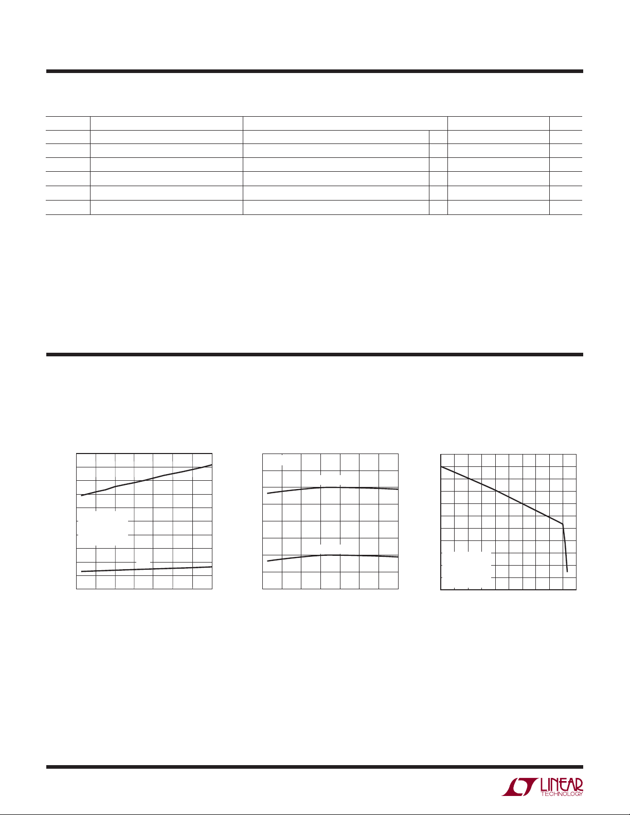
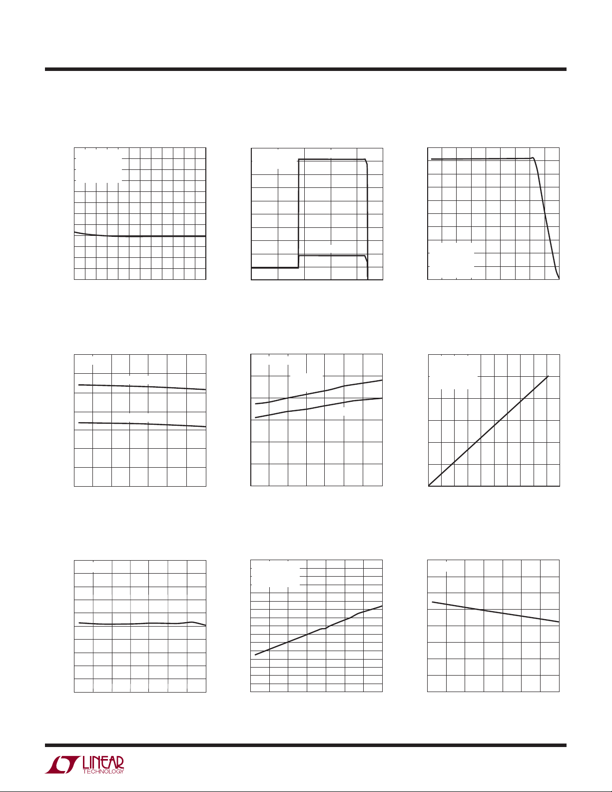
TYPICAL PERFORMANCE CHARACTERISTICS
Suspend State Supply and BAT
Currents vs Temperature
10
9
8
7
6
VCC = 5V
5
BAT = 4.2V
SUSP = 5V
4
CURRENT (μA)
EN1 = EN2 = 0V
3
2
1
0
–55
–35
I
VCC
I
BAT
25
5
–15
TEMPERATURE (°C)
65
85
3559 G01
45
Battery Regulation (Float)
Voltage vs Temperature
4.250
VCC = 5V
4.225
4.200
4.175
(V)
4.150
FLOAT
V
4.125
4.100
4.075
4.050
–35 –15 25
–55
LTC3559
LTC3559-1
TEMPERATURE (°C)
5
45 65 85
supply current does not include current through the PROG pin
BAT
where I
is the charge current.
BAT
is expressed as a fraction of measured full charge current
Battery Regulation (Float) Voltage
vs Battery Charge Current,
Constant-Voltage Charging
4.205
4.200
4.195
4.190
4.185
4.180
(V)
BAT
4.175
V
4.170
4.165
VCC = 5V
4.160
HPWR = 5V
= 845Ω
R
PROG
4.155
EN1 = EN2 = 0V
4.150
3559 G02
100
300
400
2000
I
BAT
500
(mA)
600
700
800
900
3559 G03
1000
4
3559fb
TYPICAL PERFORMANCE CHARACTERISTICS
Battery Charge Current
vs Supply Voltage
500
VCC = 5V
495
HPWR = 5V
490
485
480
475
(mA)
470
BAT
I
465
460
455
450
445
440
= 1.74k
R
PROG
EN1 = EN2 = 0V
4.3
4.5
4.6 4.9 5.1
4.8 5.0 5.2 5.4 5.5
4.7
VCC (V)
Battery Charger Undervoltage
Lockout Threshold vs Temperature
4.2
BAT = 3.5V
(V)
CC
V
4.1
4.0
3.9
3.8
3.7
3.6
RISING
FALLING
5.34.4
3559 G04
Battery Charge Current
vs Battery Voltage (LTC3559)
500
450
400
350
300
(mA)
250
BAT
I
200
150
100
50
0
2
VCC = 5V
R
PROG
= 1.74k
2.5
HPWR = 5V
HPWR = 0V
3
V
BAT
Battery Drain Current in
Undervoltage Lockout
vs Temperature
3.0
EN1 = EN2 = 0V
(μA)
BAT
I
2.5
2.0
1.5
1.0
0.5
BAT = 4.2
(LTC3559)
3.5
(V)
BAT = 3.6
LTC3559/LTC3559-1
Battery Charge Current
vs Ambient Temperature in
Thermal Regulation
500
450
400
350
300
(mA)
250
BAT
I
200
150
VCC = 5V
100
HPWR = 5V
= 1.74k
R
PROG
50
EN1 = EN2 = 0
0
–35 5
–55
4
4.5
3559 G05
–15
25
TEMPERATURE (°C)
PROG Voltage
vs Battery Charge Current
1.2
VCC = 5V
HPWR = 5V
(V)
PROG
V
1.0
0.8
0.6
0.4
0.2
= 1.74k
R
PROG
EN1 = EN2 = 0V
85
45 125
105
65
3.5
–55
–35 –15
TEMPERATURE (°C)
Recharge Threshold
vs Temperature
115
VCC = 5V
111
107
103
99
(mV)
95
91
RECHARGE
V
87
83
79
75
–55
–35
–15
TEMPERATURE (°C)
25 65 85
545
3559 G07
25
5
45
65
3559 G10
0
–55
–35 –15
TEMPERATURE (°C)
25 65 85
545
3559 G08
Battery Charger FET
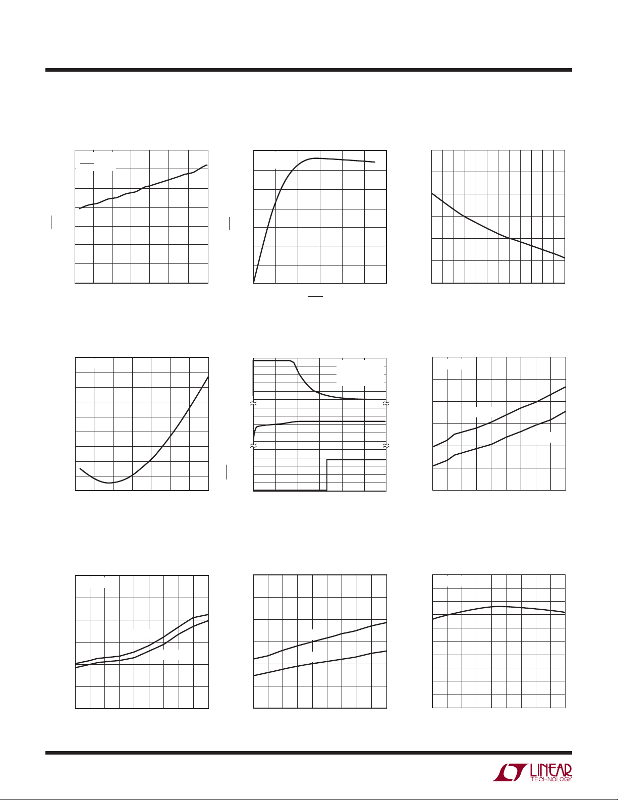
On-Resistance vs Temperature
700
VCC = 4V
= 200mA
I
BAT
650
EN1 = EN2 = 0V
600
550
(mΩ)
500
ON
R
450
400
350
300
85
–55
–15 5 25 45 65
–35
TEMPERATURE (°C)
85
3559 G11
0
100 200 300 400
I
BAT
SUSP/HPWR Pin Rising
Thresholds vs Temperature
1.2
VCC = 5V
1.1
1.0
0.9
0.8
0.7
THRESHOLD (V)
0.6
0.5
0.4
–35 –15 25
–55
5
TEMPERATURE (°C)
(mA)
500500 150 250 350 450
3559 G09
45 65 85
3559 G12
3559fb
5
LTC3559/LTC3559-1
TYPICAL PERFORMANCE CHARACTERISTICS
CHRG Pin Output Low Voltage
vs Temperature
140
VCC = 5V
I
CHRG
120
100
80
(mV)
60
CHRG
V
40
20
= 5mA
CHRG Pin I-V Curve
70
VCC = 5V
BAT = 3.8V
60
50
40
(mA)
30
CHRG
I
20
10
Timer Accuracy vs Supply Voltage
2.0
1.5
1.0
0.5
0
PERCENT ERROR (%)
–0.5
0
–55
–35 –15
TEMPERATURE (°C)
25 65 85
545
Timer Accuracy vs Temperature
7
VCC = 5V
6
5
4
3
2
1
PERCENT ERROR (%)
0
–1
–2
–55
–15
–35
TEMPERATURE (°C)
585
25
Buck Regulator Input Current vs
Temperature, Pulse Skip Mode
(LTC3559)
400
VFB = 0.82V
350
300
250
200
INPUT CURRENT (μA)
150
100
–35 5
–55
PVIN = 4.2V
–15
25
TEMPERATURE (°C)
PVIN = 2.7V
45 125
65
45 65
85
3559 G13
3559 G16
105
3559 G19
0
0
12
CHRG (V)
Complete Charge Cycle
2400mAh Battery (LTC3559)
1000
800
600
(mA)BAT (V)CHRG (V)
400
BAT
I
200
0
5.0
4.5
4.0
3.5
3.0
5.0
4.0
3.0
2.0
1.0
0
0
12 4 6
TIME (HOUR)
46
35
3559 G14
VCC = 5V
= 0.845k
R
PROG
HPWR = 5V
35
3559 G17
–1.0
4.3
4.7 4.9 5.1
4.5
Buck Regulator Input Current vs
Temperature, Burst Mode Operation
50
VFB = 0.82V
45
40
PVIN = 4.2V
35
30
INPUT CURRENT (μA)
25
20
–35 5
–55
–15
TEMPERATURE (°C)
Buck Regulator PVIN Undervoltage
Thresholds vs Temperature Frequency vs Temperature
2.5
2.4
2.3
2.2
2.1
2.0
(MHz)
OSC
1.9
f
1.8
1.7
1.6
1.5
–55
PVIN = 3.8V
–35 –15 25
TEMPERATURE (°C)
5
(V)
IN
PV
2.85
2.75
2.65
2.55
2.45
2.35
2.25
–35 5
–55
RISING
FALLING
–15
25
TEMPERATURE (°C)
85
45 125
105
65
3559 G20
VCC (V)
PVIN = 2.7V
85
45 125
65
25
85
45
65
5.3 5.5
3559 G15
105
3559 G18
105
125
3559 G21
3559fb
6
TYPICAL PERFORMANCE CHARACTERISTICS
5
5
0
0
LTC3559/LTC3559-1
Buck Regulator Enable
Thresholds vs Temperature
1200
PVIN = 3.8V
1100
1000
900
(mV)
800
EN
V
700
600
500
400
–35 125
–55
–15
RISING
FALLING
25
45
5
TEMPERATURE (°C)
Buck Regulator Effi ciency vs I
105
65
85
3559 G22
LOAD
Buck Regulator PMOS R
vs Temperature (LTC3559)
1300
1200
1100
1000
900
(mΩ)
800
DS(ON)
R
700
600
500
400
–55
–35
–15
PVIN = 2.7V
5
TEMPERATURE (°C)
PVIN = 4.2V
25
45 12
(LTC3559) Buck Regulator Load Regulation
100
Burst Mode
90
OPERATION
80
70
60
50
40
EFFICIENCY (%)
30
20
10
0
0.1 10 100 1000
1
I
LOAD
PULSE SKIP
MODE
(mA)
V
OUT
PV
= 2.5V
= 4.2V
IN
3559 G25
(V)
OUT
V
2.60
2.58
2.56
2.54
2.52
2.50
2.48
2.46
2.44
PVIN = 3.8V
= 2.5V
V
OUT
1
Burst Mode
OPERATION
PULSE SKIP
MODE
10 100 100
I
(mA)
LOAD
65
DS(0N)
85
105
3559 G23
3559 G26
Buck Regulator NMOS R
vs Temperature (LTC3559)
1300
1200
1100
1000
900
(mΩ)
800
DS(ON)
R
700
600
500
400
–55
PVIN = 2.7V
–35
–15
PVIN = 4.2V
5
25
TEMPERATURE (°C)
45 12
Buck Regulator Line Regulation
2.60
V
= 2.5V
OUT
= 200mA
I
LOAD
2.58
2.56
2.54
(V)
2.52
OUT
V
2.50
2.48
2.46
2.44
3.0 3.3 3.9
2.7
3.6
PVIN (V)
65
DS(0N)
85
105
3559 G24
4.2
3559 G27
Buck Regulator Effi ciency vs I
(LTC3559)
100
Burst Mode
90
OPERATION
80
70
60
50
40
EFFICIENCY (%)
30
20
10
0
0.1 10 100 1000
PULSE SKIP
MODE
V
OUT
PVIN = 2.7V
PV
1
I
(mA)
LOAD
= 1.2V
= 4.2V
IN
LOAD
3559 G28
Buck Regulator Load Regulation
1.25
PVIN = 3.8V
(V)
OUT
V
1.24
1.23
1.22
1.21
1.20
1.19
1.18
1.17
1.16
1.15
= 1.2V
V
OUT
Burst Mode
OPERATION
PULSE SKIP
MODE
1
10 100 100
I
(mA)
LOAD
3559 G29
Buck Regulator Line Regulation
1.25
V
= 1.2V
OUT
(V)
OUT
V
1.24
1.23
1.22
1.21
1.20
1.19
1.18
1.17
1.16
1.15
2.7
I
LOAD
= 200mA
3.0
3.3
PVIN (V)
3.6
3.9
4.2
3559 G30
3559fb
7
LTC3559/LTC3559-1
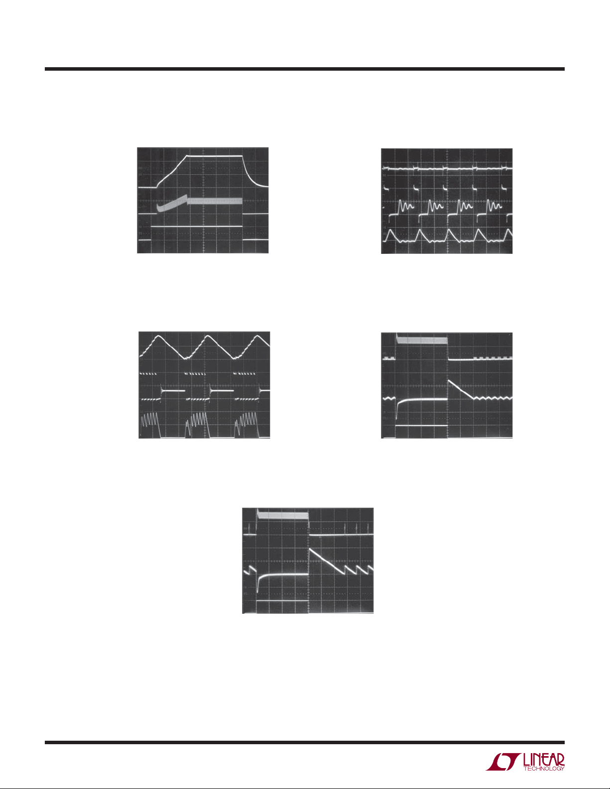
TYPICAL PERFORMANCE CHARACTERISTICS
Buck Regulator Start-Up Transient
Buck Regulator Pulse Skip Mode
Operation
V
500mV/DIV
INDUCTOR
CURRENT
= 200mA/DIV
I
L
2V/DIV
V
20mV/DIV (AC)
2V/DIV
INDUCTOR
CURRENT
= 60mA/DIV
I
L
OUT
EN
= 3.8V
PV
IN
PULSE SKIP MODE
LOAD = 6Ω
50μs/DIV
Buck Regulator Burst Mode
Operation
OUT
SW
= 3.8V
PV
IN
LOAD = 60mA
2μs/DIV
3559 G33
3559 G35
V
SW
2V/DIV
INDUCTOR
CURRENT
= 50mA/DIV
I
L
INDUCTOR
CURRENT
= 200mA/DIV
V
LOAD STEP
OUT
OUT
20mV/DIV (AC)
I
L
50mV/DIV (AC)
5mA TO 290mA
= 3.8V
PV
IN
LOAD = 10mA
200ns/DIV
Buck Regulator Transient
Response, Pulse Skip Mode
= 3.8V 50μs/DIV
PV
IN
3559 G34
3559 G36
8
INDUCTOR
CURRENT
= 200mA/DIV
I
L
V
50mV/DIV (AC)
5mA TO 290mA
OUT
LOAD STEP
Buck Regulator Transient
Response, Burst Mode Operation
= 3.8V 50μs/DIV
PV
IN
3559 G37
3559fb

PIN FUNCTIONS
LTC3559/LTC3559-1
GND (Pin 1): Ground, Connect to Exposed Pad (Pin 17).
BAT (Pin 2): Charge Current Output. Provides charge cur-
rent to the battery and regulates fi nal fl oat voltage to 4.2V
(LTC3559) or 4.1V (LTC3559-1).
MODE (Pin 3): MODE Pin for Buck Regulators. When held
high, both regulators are in Burst Mode operation. When
held low both regulators operate in pulse skip mode. This
pin is a high impedance input; do not fl oat.
FB1 (Pin 4): Buck 1 Feedback Voltage Pin. Receives feedback by a resistor divider connected across the output.
EN1 (Pin 5): Enable Input Pin for Buck 1. This pin is a high
impedance input; do not fl oat. Active high.
SW1 (Pin 6): Buck 1 Switching Node. External inductor
connects to this node.
(Pin 7): Input Supply Pin for Buck Regulators.
PV
IN
Connect to BAT. A 2.2μF decoupling capacitor to GND is
recommended.
SW2 (Pin 8): Buck 2 Switching Node. External inductor
connects to this node.
can toggle between low power and high power modes per
USB specifi cation. A weak pull-down current is internally
applied to this pin to ensure it is low at power up when
the input is not being driven externally.
NTC (Pin 13): Input to the NTC Thermistor Monitoring
Circuit. The NTC pin connects to a negative temperature
coeffi cient thermistor which is typically co-packaged with
the battery pack to determine if the battery is too hot or
too cold to charge. If the battery temperature is out of
range, charging is paused until the battery temperature
re-enters the valid range. A low drift bias resistor is required from V
NTC to ground. To disable the NTC function, the NTC pin
should be grounded.
PROG (Pin 14): Charge Current Program and Charge
Current Monitor Pin. Charge current is programmed by
connecting a resistor from PROG to ground. When charging in constant-current mode, the PROG pin servos to 1V
if the HPWR pin is pulled high, or 200mV if the HPWR pin
is pulled low. The voltage on this pin always represents
the battery current through the following formula:
to NTC and a thermistor is required from
CC
EN2 (Pin 9): Enable Input Pin for Buck 2. This pin is a high
impedance input; do not fl oat. Active high.
FB2 (Pin 10): Buck 2 Feedback Voltage Pin. Receives feedback by a resistor divider connected across the output.
SUSP (Pin 11): Suspend Battery Charging Operation.
A voltage greater than 1.2V on this pin puts the battery
charger into suspend mode, disables the charger and
resets the termination timer. A weak pull-down current is
internally applied to this pin to ensure it is low at power
up when the input is not being driven externally.
HPWR (Pin 12): High Current Battery Charging Enabled.
A voltage greater than 1.2V at this pin programs the
BAT pin current at 100% of the maximum programmed
charge current. A voltage less than 0.4V sets the BAT pin
current to 20% of the maximum programmed charge
current. When used with a 1.74k PROG resistor, this pin
I
CHRG (Pin 15): Open-Drain Charge Status Output. The
CHRG pin indicates the status of the battery charger. Four
possible states are represented by CHRG: charging, not
charging (i.e., the charge current is less than 1/10th of the
full-scale charge current), unresponsive battery (i.e., the
battery voltage remains below 2.9V after 1/2 hour of charging) and battery temperature out of range. CHRG requires
a pull-up resistor and/or LED to provide indication.
V
CC
capacitor to GND is recommended.
Exposed Pad (Pin 17): Ground. The Exposed Pad must
be soldered to PCB ground to provide electrical contact
and rated thermal performance.
PROG
= •800
BAT
R
PROG
(Pin 16): Battery Charger Input. A 1μF decoupling
3559fb
9

LTC3559/LTC3559-1
BLOCK DIAGRAM
CHRG
15
HPWR
12
SUSP
11
NTC
13
MODE
3
EN1
5
EN2
9
FB1
4
TEMPERATURE
BANDGAP
UNDERVOLTAGE
LOCKOUT
DIE
16
V
CC
BAT
V
IN
BODY
MAXER
TA
T
DIE
–
G
m
+
CLK
V
C
0.8V
CA
V
FB
LOGIC
NTCA
NTC REF
OT
T
DIE
V
REF
800x
1x
–
+
BATTERY CHARGER
MODEEN
CONTROL
LOGIC
BUCK REGULATOR 1
BAT
PROG
PV
SW1
2
14
IN
7
6
10
OSCILLATOR
2.25MHz
FB2
10
CLK
V
–
FB
G
m
+
0.8V
GND EXPOSED PAD
1 17
CLK
V
C
MODEEN
CONTROL
LOGIC
BUCK REGULATOR 2
SW2
8
3559 BD
3559fb

OPERATION
LTC3559/LTC3559-1
The LTC3559/LTC3559-1 are linear battery chargers with
dual monolithic synchronous buck regulators. The buck
regulators are internally compensated and need no external
compensation components.
The battery charger employs a constant- current/constantvoltage charging algorithm and is capable of charging a
single Li-Ion battery at charging currents up to 950mA. The
user can program the maximum charging current available
USB (5V)
R
PROG
1.62k
LOW (PULSE SKIP MODE)
HIGH
HIGH
HIGH
V
CC
PROG
SUSP
HPWR
EN1
EN2
MODE
LTC3559/
LTC3559-1
at the BAT pin via a single PROG resistor. The actual BAT
pin current is set by the status of the HPWR pin.
For proper operation, the BAT and PV
pins must be tied
IN
together. If a buck regulator is also enabled during the
battery charging operation, the net current charging the
battery may be lower than the actual programmed value.
Refer to Figure 1 for an explanation.
500mA
300mA
BAT
PV
SW1
SW2
IN
200mA
+
3559 F01
2.2μF
V
OUT1
V
OUT2
+
SINGLE Li-lon
CELL 3.6V
Figure 1. Current Being Delivered at the BAT Pin Is 500mA. Both Buck Regulators Are Enabled. The Sum of the
Average Input Currents Drawn by Both Buck Regulators Is 200mA. This Makes the Effective Battery Charging Current
Only 300mA. If the HPWR Pin Were Tied LO, the BAT Pin Current Would Be 100mA. With the Buck Regulator
Conditions Unchanged, This Would Cause the Battery to Discharge at 100mA
APPLICATIONS INFORMATION
Battery Charger Introduction
The LTC3559/LTC3559-1 have a linear battery charger
designed to charge single-cell lithium-ion batteries. The
charger uses a constant-current/constant-voltage charge
algorithm with a charge current programmable up to
950mA. Additional features include automatic recharge,
an internal termination timer, low-battery trickle charge
conditioning, bad-battery detection, and a thermistor
sensor input for out of temperature charge pausing.
Furthermore, the battery charger is capable of operating
from a USB power source. In this application, charge
current can be programmed to a maximum of 100mA or
500mA per USB power specifi cations.
Input Current vs Charge Current
The battery charger regulates the total current delivered
to the BAT pin; this is the charge current. To calculate the
total input current (i.e., the total current drawn from the
pin), it is necessary to sum the battery charge current,
V
CC
charger quiescent current and PROG pin current.
Undervoltage Lockout (UVLO)
The undervoltage lockout circuit monitors the input voltage (V
above V
) and disables the battery charger until VCC rises
CC
(typically 4V). 200mV of hysteresis prevents
UVLO
oscillations around the trip point. In addition, a differential
undervoltage lockout circuit disables the battery charger
when V
falls to within V
CC
(typically 50mV) of the
DUVLO
BAT voltage.
3559fb
11

LTC3559/LTC3559-1
APPLICATIONS INFORMATION
Suspend Mode
The battery charger can also be disabled by pulling the
SUSP pin above 1.2V. In suspend mode, the battery
drain current is reduced to 1.5μA and the input current is
reduced to 8.5μA.
Charge Cycle Overview
When a battery charge cycle begins, the battery charger
fi rst determines if the battery is deeply discharged. If the
battery voltage is below V
, typically 2.9V, an automatic
TRKL
trickle charge feature sets the battery charge current to
10% of the full-scale value.
Once the battery voltage is above 2.9V, the battery charger
begins charging in constant-current mode. When the
battery voltage approaches the 4.2V (LTC3559) or 4.1V
(LTC3559-1) required to maintain a full charge, otherwise
known as the fl oat voltage, the charge current begins to
decrease as the battery charger switches into constantvoltage mode.
mode, the 4-hour timer is started. After the safety timer
expires, charging of the battery will discontinue and no
more current will be delivered.
Automatic Recharge
After the battery charger terminates, it will remain off,
drawing only microamperes of current from the battery.
If the portable product remains in this state long enough,
the battery will eventually self discharge. To ensure that the
battery is always topped off, a charge cycle will automatically begin when the battery voltage falls below V
RECHRG
. In
the event that the safety timer is running when the battery
voltage falls below V
RECHRG
prevent brief excursions below V
safety timer, the battery voltage must be below V
, it will reset back to zero. To
RECHRG
from resetting the
RECHRG
for more than 1.7ms. The charge cycle and safety timer
will also restart if the V
then high (e.g., V
CC
UVLO or DUVLO cycles low and
CC
is removed and then replaced) or the
charger enters and then exits suspend mode.
Programming Charge Current
Trickle Charge and Defective Battery Detection
Any time the battery voltage is below V
, the charger
TRKL
goes into trickle charge mode and reduces the charge
current to 10% of the full-scale current. If the battery
voltage remains below V
for more than 1/2 hour, the
TRKL
charger latches the bad-battery state, automatically terminates, and indicates via the CHRG pin that the battery was
unresponsive. If for any reason the battery voltage rises
above V
, the charger will resume charging. Since the
TRKL
charger has latched the bad-battery state, if the battery
voltage then falls below V
V
RECHRG
fi rst, the charger will immediately assume that
again but without rising past
TRKL
the battery is defective. To reset the charger (i.e., when
the dead battery is replaced with a new battery), simply
remove the input voltage and reapply it or put the part in
and out of suspend mode.
Charge Termination
The battery charger has a built-in safety timer that sets the
total charge time for 4 hours. Once the battery voltage rises
above V
RECHRG
and the charger enters constant-voltage
The PROG pin serves both as a charge current program
pin, and as a charge current monitor pin. By design, the
PROG pin current is 1/800th of the battery charge current.
Therefore, connecting a resistor from PROG to ground
programs the charge current while measuring the PROG pin
voltage allows the user to calculate the charge current.
Full-scale charge current is defi ned as 100% of the constant-current mode charge current programmed by the
PROG resistor. In constant-current mode, the PROG pin
servos to 1V if HPWR is high, which corresponds to charging at the full-scale charge current, or 200mV if HPWR
is low, which corresponds to charging at 20% of the fullscale charge current. Thus, the full-scale charge current
and desired program resistor for a given full-scale charge
current are calculated using the following equations:
800
I
=
CHG
R
PROG
R
=
PROG
800
I
CHG
V
V
12
3559fb

APPLICATIONS INFORMATION
LTC3559/LTC3559-1
In any mode, the actual battery current can be determined
by monitoring the PROG pin voltage and using the following equation:
I
BAT
PROG
= •800
R
PROG
Thermal Regulation
To prevent thermal damage to the IC or surrounding
components, an internal thermal feedback loop will automatically decrease the programmed charge current if the
die temperature rises to approximately 115°C. Thermal
regulation protects the battery charger from excessive
temperature due to high power operation or high ambient
thermal conditions and allows the user to push the limits
of the power handling capability with a given circuit board
design without risk of damaging the LTC3559/LTC3559-1
or external components. The benefi t of the LTC3559/
LTC3559-1 battery charger thermal regulation loop is that
charge current can be set according to actual conditions
rather than worst-case conditions with the assurance that
the battery charger will automatically reduce the current
in worst-case conditions.
Charge Status Indication
The CHRG pin indicates the status of the battery charger.
Four possible states are represented by CHRG: charging,
not charging, unresponsive battery and battery temperature
out of range.
The signal at the CHRG pin can be easily recognized as one
of the above four states by either a human or a microprocessor. The CHRG pin, which is an open-drain output, can
drive an indicator LED through a current limiting resistor
for human interfacing, or simply a pull-up resistor for
microprocessor interfacing.
To make the CHRG pin easily recognized by both humans
and microprocessors, the pin is either low for charging,
high for not charging, or it is switched at high frequency
(35kHz) to indicate the two possible faults: unresponsive
battery and battery temperature out of range.
When charging begins, CHRG is pulled low and remains
low for the duration of a normal charge cycle. When the
charge current has dropped to below 10% of the full-scale
current, the CHRG pin is released (high impedance). If a
fault occurs after the CHRG pin is released, the pin remains high impedance. However, if a fault occurs before
the CHRG pin is released, the pin is switched at 35kHz.
While switching, its duty cycle is modulated between a high
and low value at a very low frequency. The low and high
duty cycles are disparate enough to make an LED appear
to be on or off thus giving the appearance of “blinking”.
Each of the two faults has its own unique “blink” rate for
human recognition as well as two unique duty cycles for
microprocessor recognition.
Table 1 illustrates the four possible states of the CHRG
pin when the battery charger is active.
Table 1. CHRG Output Pin
MODULATION
STATUS FREQUENCY
Charging 0Hz 0 Hz (Lo-Z) 100%
< C/10 0Hz 0 Hz (Hi-Z) 0%
I
BAT
NTC Fault
Bad Battery
35kHz
35kHz
(BLINK)
FREQUENCY DUTY CYCLE
1.5Hz at 50% 6.25% to 93.75%
6.1Hz at 50% 12.5% to 87.5%
An NTC fault is represented by a 35kHz pulse train whose
duty cycle varies between 6.25% and 93.75% at a 1.5Hz
rate. A human will easily recognize the 1.5Hz rate as a
“slow” blinking which indicates the out of range battery
temperature while a microprocessor will be able to decode
either the 6.25% or 93.75% duty cycles as an NTC fault.
If a battery is found to be unresponsive to charging (i.e.,
its voltage remains below V
for over 1/2 hour), the
TRKL
CHRG pin gives the battery fault indication. For this fault,
a human would easily recognize the frantic 6.1Hz “fast”
blinking of the LED while a microprocessor would be able
to decode either the 12.5% or 87.5% duty cycles as a bad
battery fault.
Although very improbable, it is possible that a duty cycle
reading could be taken at the bright-dim transition (low
duty cycle to high duty cycle). When this happens the
duty cycle reading will be precisely 50%. If the duty cycle
reading is 50%, system software should disqualify it and
take a new duty cycle reading.
3559fb
13

LTC3559/LTC3559-1
APPLICATIONS INFORMATION
NTC Thermistor
The battery temperature is measured by placing a negative temperature coeffi cient (NTC) thermistor close to the
battery pack. The NTC circuitry is shown in Figure 3.
To use this feature, connect the NTC thermistor, R
between the NTC pin and ground, and a bias resistor, R
from V
to NTC. R
CC
should be a 1% resistor with a
NOM
NTC
NOM
,
,
value equal to the value of the chosen NTC thermistor at
25°C (R25). A 100k thermistor is recommended since
thermistor current is not measured by the battery charger
and its current will have to be considered for compliance
with USB specifi cations.
The battery charger will pause charging when the resistance of the NTC thermistor drops to 0.54 times the
POWER
ON
FAULT
BAT b 2.9V
DUVLO, UVLO AND SUSPEND DISABLE MODE
IF SUSP < 0.4V AND
> 4V AND
V
CC
> BAT + 130mV
V
CC
BATTERY CHARGING SUSPENDED
CHRG PULSES
value of R25 or approximately 54k (for a Vishay “Curve
1” thermistor, this corresponds to approximately 40°C). If
the battery charger is in constant-voltage mode, the safety
timer will pause until the thermistor indicates a return to
a valid temperature.
As the temperature drops, the resistance of the NTC
thermistor rises. The battery charger is also designed
to pause charging when the value of the NTC thermistor
increases to 3.25 times the value of R25. For a Vishay
“Curve 1” thermistor, this resistance, 325k, corresponds
to approximately 0°C. The hot and cold comparators each
have approximately 3°C of hysteresis to prevent oscillation
about the trip point. Grounding the NTC pin disables all
NTC functionality.
NO
CHRG HIGH IMPEDANCE
YES
NTC FAULT
NO FAULT
2.9V < BAT < V
RECHRG
STANDBY MODE
NO CHARGE CURRENT
CHRG HIGH IMPEDANCE
14
TRICKLE CHARGE MODE
1/10 FULL CHARGE CURRENT
CHRG STRONG PULL-DOWN
30 MINUTE TIMER BEGINS
30 MINUTE
TIMEOUT
DEFECTIVE BATTERY
NO CHARGE CURRENT
CHRG PULSES
Figure 2. State Diagram of the Battery Charger Operation
BAT > 2.9V
CONSTANT CURRENT MODE
FULL CHARGE CURRENT
CHRG STRONG PULL-DOWN
CONSTANT VOLTAGE MODE
4-HOUR TERMINATION TIMER
BEGINS
BAT DROPS BELOW V
4-HOUR TERMINATION TIMER RESETS
4-HOUR
TIMEOUT
RECHRG
3559 F02
3559fb

APPLICATIONS INFORMATION
LTC3559/LTC3559-1
Alternate NTC Thermistors and Biasing
The battery charger provides temperature qualifi ed
charging if a grounded thermistor and a bias resistor are
connected to the NTC pin. By using a bias resistor whose
value is equal to the room temperature resistance of the
thermistor (R25) the upper and lower temperatures are
pre-programmed to approximately 40°C and 0°C, respectively (assuming a Vishay “Curve 1” thermistor).
The upper and lower temperature thresholds can be adjusted by either a modifi cation of the bias resistor value
or by adding a second adjustment resistor to the circuit.
If only the bias resistor is adjusted, then either the upper
or the lower threshold can be modifi ed but not both. The
other trip point will be determined by the characteristics
of the thermistor. Using the bias resistor in addition to an
adjustment resistor, both the upper and the lower temperature trip points can be independently programmed with
the constraint that the difference between the upper and
lower temperature thresholds cannot decrease. Examples
of each technique are given below.
NTC thermistors have temperature characteristics which
are indicated on resistance-temperature conversion tables.
The Vishay-Dale thermistor NTHS0603N011-N1003F, used
in the following examples, has a nominal value of 100k
and follows the Vishay “Curve 1” resistance-temperature
characteristic.
In the explanation below, the following notation is used.
R25 = Value of the thermistor at 25°C
R
NTC|COLD
R
NTC|HOT
r
COLD
r
HOT
R
NOM
= Value of thermistor at the cold trip point
= Value of the thermistor at the hot trip point
= Ratio of R
= Ratio of R
NTC|COLD
NTC|HOT
to R25
to R25
= Primary thermistor bias resistor (see Figure 3)
R1 = Optional temperature range adjustment resistor (see
Figure 4)
The trip points for the battery charger’s temperature qualifi cation are internally programmed at 0.349 • V
hot threshold and 0.765 • V
for the cold threshold.
CC
for the
CC
Therefore, the hot trip point is set when:
R
NTC HOT
+
RR
NOM NTCHOT
|
•.•
= 0 349
VV
|
CC CC
and the cold trip point is set when:
R
NTC COLD
+
RR
NOM NTC COLD
|
•.•
= 0 765
VV
|
CC CC
R
NOM
100k
R
100k
NTC
16
13
V
CC
NTC
(NTC FALLING)
0.765 • V
(NTC RISING)
0.349 • V
(NTC FALLING)
0.017 • V
NTC BLOCK
CC
CC
CC
V
CC
16
0.765 • V
CC
NTC
(NTC FALLING)
(NTC RISING)
0.349 • V
CC
(NTC FALLING)
0.017 • V
CC
–
TOO_COLD
+
–
TOO_HOT
+
+
NTC_ENABLE
–
–
TOO_COLD
+
R
NOM
105k
R1
12.7k
13
–
R
NTC
TOO_HOT
100k
+
+
NTC_ENABLE
–
3559 F03
Figure 3. Typical NTC Thermistor Circuit Figure 4. NTC Thermistor Circuit with Additional Bias Resistor
3559 F04
3559fb
15

LTC3559/LTC3559-1
Y
APPLICATIONS INFORMATION
Solving these equations for R
NTC|COLD
and R
NTC|HOT
results in the following:
R
NTC|HOT
= 0.536 • R
NOM
and
R
NTC|COLD
By setting R
in r
HOT
= 3.25 • R
equal to R25, the above equations result
NOM
= 0.536 and r
NOM
= 3.25. Referencing these ratios
COLD
to the Vishay Resistance-Temperature Curve 1 chart gives
a hot trip point of about 40°C and a cold trip point of about
0°C. The difference between the hot and cold trip points
is approximately 40°C.
By using a bias resistor, R
, different in value from
NOM
R25, the hot and cold trip points can be moved in either
direction. The temperature span will change somewhat due
to the nonlinear behavior of the thermistor. The following
equations can be used to easily calculate a new value for
the bias resistor:
r
=
HOT
0 536
.
R
25
•
R
NOM
For example, to set the trip points to 0°C and 45°C with
a Vishay Curve 1 thermistor choose:
3 266 0 4368
Rkk
NOM
.–.
==
2 714
.
100 104 2
•.
the nearest 1% value is 105k.
R1 = 0.536 • 105k – 0.4368 • 100k = 12.6k
the nearest 1% value is 12.7k. The fi nal solution is shown
in Figure 4 and results in an upper trip point of 45°C and
a lower trip point of 0°C.
USB and Wall Adapter Power
Although the battery charger is designed to draw power
from a USB port to charge Li-Ion batteries, a wall adapter
can also be used. Figure 5 shows an example of how to
combine wall adapter and USB power inputs. A P-channel
MOSFET, MP1, is used to prevent back conduction into
the USB port when a wall adapter is present and Schottky
diode, D1, is used to prevent USB power loss through the
1k pull-down resistor.
r
HOT
=
and r
COLD
325
.
R
25
•
are the resistance ratios at the
COLD
de-
R
NOM
where r
hot and cold trip points. Note that these equations
sired
are linked. Therefore, only one of the two trip points can
be chosen, the other is determined by the default ratios
designed in the IC. Consider an example where a 60°C
hot trip point is desired.
From the Vishay Curve 1 R-T characteristics, r
at 60°C. Using the above equation, R
to 46.4k. With this value of R
NOM
NOM
, the cold trip point is
is 0.2488
HOT
should be set
about 16°C. Notice that the span is now 44°C rather than
the previous 40°C.
The upper and lower temperature trip points can be independently programmed by using an additional bias resistor
as shown in Figure 4. The following formulas can be used
•
NOM
R
25
and R1:
to compute the values of R
rr
–
R
NOM
COLD HOT
=
.
2 714
Typically, a wall adapter can supply signifi cantly more
current than the 500mA-limited USB port. Therefore, an
N-channel MOSFET, MN1, and an extra program resistor are
used to increase the maximum charge current to 950mA
when the wall adapter is present.
5V WALL
ADAPTER
950mA I
CHG
USB
POWER
500mA I
Figure 5. Combining Wall Adapter and USB Power
CHG
MP1
D1
BATTERY
CHARGER
V
CC
PROG
1.65k
MN1
1k
BAT
I
BAT
1.74k
+
Li-Ion
BATTER
3559 F05
RRr
=
.• – •
1 0 536 RR25
NOM HOT
16
3559fb

APPLICATIONS INFORMATION
LTC3559/LTC3559-1
Power Dissipation
The conditions that cause the LTC3559/LTC3559-1 to
reduce charge current through thermal feedback can be
approximated by considering the power dissipated in the
IC. For high charge currents, the LTC3559/LTC3559-1
power dissipation is approximately:
PVV I
=
D CC BAT BAT
where PD is the power dissipated, VCC is the input supply
voltage, V
current. It is not necessary to perform any worst-case power
dissipation scenarios because the LTC3559/LTC3559-1
will automatically reduce the charge current to maintain
the die temperature at approximately 105°C. However, the
approximate ambient temperature at which the thermal
feedback begins to protect the IC is:
TCP
=°
ADJA
TCVVI
=°
A CC BAT BAT JA
Example: Consider an LTC3559/LTC3559-1 operating from
a USB port providing 500mA to a 3.5V Li-Ion battery.
The ambient temperature above which the LTC3559/
LTC3559-1 will begin to reduce the 500mA charge current is approximately:
TCVVmACW
=°
A
TC
=°
A
=°
TC
A
The LTC3559/LTC3559-1 can be used above 70°C, but
the charge current will be reduced from 500mA. The
approximate current at a given ambient temperature can
be calculated:
I
BAT
Using the previous example with an ambient temperature of 88°C, the charge current will be reduced to
approximately:
I
BAT
–•
()
is the battery voltage, and I
BAT
105
105––– ••
105 5 3 5 500 68
105 0
54
=
VV
()
CC BAT JA
=
VV CWCCA
535 68
()
θ
()
––.• • /
()()
–.. • / –75 68 105 51
CT
°
105 –
–•θ
CC
°°
105 88
–. • / /
–
°=° °
WCW C
A
°
=
θ
102
17
BAT
°
°
is the charge
°
Furthermore, the voltage at the PROG pin will change
proportionally with the charge current as discussed in
the Programming Charge Current section.
It is important to remember that LTC3559/LTC3559-1
applications do not need to be designed for worst-case
thermal conditions since the IC will automatically reduce
power dissipation when the junction temperature reaches
approximately 105°C.
Battery Charger Stability Considerations
The LTC3559/LTC3559-1 battery charger contains two
control loops: the constant-voltage and constant-current loops. The constant-voltage loop is stable without
any compensation when a battery is connected with low
impedance leads. Excessive lead length, however, may add
enough series inductance to require a bypass capacitor
of at least 1.5μF from BAT to GND. Furthermore, a 4.7μF
capacitor with a 0.2Ω to 1Ω series resistor from BAT to
GND is required to keep ripple voltage low when the battery is disconnected.
High value capacitors with very low ESR (especially
ceramic) reduce the constant-voltage loop phase margin,
possibly resulting in instability. Ceramic capacitors up to
22μF may be used in parallel with a battery, but larger
ceramics should be decoupled with 0.2Ω to 1Ω of series
resistance.
In constant-current mode, the PROG pin is in the feedback
loop, not the battery. Because of the additional pole created
by the PROG pin capacitance, capacitance on this pin must
be kept to a minimum. With no additional capacitance on
the PROG pin, the charger is stable with program resistor
values as high as 25K. However, additional capacitance
on this node reduces the maximum allowed program
resistor. The pole frequency at the PROG pin should be
kept above 100kHz. Therefore, if the PROG pin is loaded
with a capacitance, C
be used to calculate the maximum resistance value for
:
R
PROG
R
PROG
≤
π ••
210
, the following equation should
PROG
1
5
C
PROG
= 167
IImA
BAT
3559fb
17

LTC3559/LTC3559-1
APPLICATIONS INFORMATION
Average, rather than instantaneous, battery current may be
of interest to the user. For example, if a switching power
supply operating in low-current mode is connected in
parallel with the battery, the average current being pulled
out of the BAT pin is typically of more interest than the
instantaneous current pulses. In such a case, a simple RC
fi lter can be used on the PROG pin to measure the average
battery current as shown in Figure 6. A 10k resistor has
been added between the PROG pin and the fi lter capacitor
to ensure stability.
LTC3559/
LTC3559-1
PROG
GND
Figure 6. Isolated Capacitive Load on PROG Pin and Filtering
R
10k
PROG
3559 F06
C
FILTER
CHARGE
CURRENT
MONITOR
CIRCUITRY
USB Inrush Limiting
When a USB cable is plugged into a portable product,
the inductance of the cable and the high-Q ceramic input
capacitor form an L-C resonant circuit. If there is not
much impedance in the cable, it is possible for the voltage
at the input of the product to reach as high as twice the
USB voltage (~10V) before it settles out. In fact, due to
the high voltage coeffi cient of many ceramic capacitors
(a nonlinearity), the voltage may even exceed twice the
USB voltage. To prevent excessive voltage from damaging
the LTC3559/LTC3559-1 during a hot insertion, the soft
connect circuit in Figure 7 can be employed.
In the circuit of Figure 7, capacitor C1 holds MP1 off when
the cable is fi rst connected. Eventually C1 begins to charge
up to the USB voltage applying increasing gate support
to MP1. The long time constant of R1 and C1 prevents
MP1
5V USB
INPUT
Si2333
C1
100nF
USB CABLE
R1
40k
Figure 7. USB Soft Connect Circuit
C2
10μF
V
CC
LTC3559/
LTC3559-1
GND
3559 F07
the current from building up in the cable too fast thus
dampening out any resonant overshoot.
Buck Switching Regulator General Information
The LTC3559/LTC3559-1 contain two 2.25MHz constantfrequency current mode switching regulators that provide
up to 400mA each. Both switchers can be programmed
for a minimum output voltage of 0.8V and can be used
to power a microcontroller core, microcontroller I/O,
memory or other logic circuitry. Both regulators support
100% duty cycle operation (dropout mode) when the
input voltage drops very close to the output voltage and
are also capable of operating in Burst Mode operation for
highest effi ciencies at light loads (Burst Mode operation
is pin selectable). The switching regulators also include
soft-start to limit inrush current when powering on, short
circuit current protection, and switch node slew limiting
circuitry to reduce radiated EMI.
A single MODE pin sets both regulators in Burst Mode
operation or pulse skip operating mode while each regulator is enabled individually through their respective enable
pins EN1 and EN2. The buck regulators input supply (PV
IN
)
should be connected to the battery pin (BAT). This allows
the undervoltage lockout circuit on the BAT pin to disable
the buck regulators when the BAT voltage drops below
2.45V. Do not drive the buck switching regulators from
a voltage other than BAT. A 2.2μF decoupling capacitor
from the PV
pin to GND is recommended.
IN
Buck Switching Regulator
Output Voltage Programming
Both switching regulators can be programmed for output
voltages greater than 0.8V. The output voltage for each
buck switching regulator is programmed using a resistor
divider from the switching regulator output connected to
the feedback pins (FB1 and FB2) such that:
V
= 0.8(1 + R1/R2)
OUT
Typical values for R1 are in the range of 40k to 1M. The
capacitor C
cancels the pole created by feedback re-
FB
sistors and the input capacitance of the FB pin and also
helps to improve transient response for output voltages
much greater than 0.8V. A variety of capacitor sizes can
be used for C
but a value of 10pF is recommended for
FB
3559fb
18

APPLICATIONS INFORMATION
LTC3559/LTC3559-1
most applications. Experimentation with capacitor sizes
between 2pF and 22pF may yield improved transient
response if so desired by the user.
Buck Switching Regulator Operating Modes
The step-down switching regulators include two possible
operating modes to meet the noise/power needs of a
variety of applications.
In pulse skip mode, an internal latch is set at the start of
every cycle, which turns on the main P-channel MOSFET
switch. During each cycle, a current comparator compares
the peak inductor current to the output of an error amplifi er.
The output of the current comparator resets the internal
latch, which causes the main P-channel MOSFET switch to
turn off and the N-channel MOSFET synchronous rectifi er
to turn on. The N-channel MOSFET synchronous rectifi er
turns off at the end of the 2.25MHz cycle or if the current
through the N-channel MOSFET synchronous rectifi er
drops to zero. Using this method of operation, the error
amplifi er adjusts the peak inductor current to deliver the
required output power. All necessary compensation is
internal to the step-down switching regulator requiring
only a single ceramic output capacitor for stability. At
light loads in pulse skip mode, the inductor current may
reach zero on each pulse which will turn off the N-channel
MOSFET synchronous rectifi er. In this case, the switch
node (SW1 or SW2) goes high impedance and the switch
node voltage will “ring”. This is discontinuous operation,
and is normal behavior for a switching regulator. At very
light loads in pulse skip mode, the step-down switching
P
VIN
EN
PWM
CONTROL
MODE
MP
MN
SW
L
V
OUT
+
C
C
FB
O
R1
regulators will automatically skip pulses as needed to
maintain output regulation. At high duty cycle (V
/2) in pulse skip mode, it is possible for the inductor
PV
IN
OUT
>
current to reverse causing the buck converter to switch
continuously. Regulation and low noise operation are
maintained but the input supply current will increase to a
couple mA due to the continuous gate switching.
During Burst Mode operation, the step-down switching
regulators automatically switch between fi xed frequency
PWM operation and hysteretic control as a function of
the load current. At light loads the step-down switching
regulators control the inductor current directly and use a
hysteretic control loop to minimize both noise and switching
losses. During Burst Mode operation, the output capacitor
is charged to a voltage slightly higher than the regulation
point. The step-down switching regulator then goes into
sleep mode, during which the output capacitor provides
the load current. In sleep mode, most of the switching
regulator’s circuitry is powered down, helping conserve
battery power. When the output voltage drops below a
pre-determined value, the step-down switching regulator
circuitry is powered on and another burst cycle begins. The
sleep time decreases as the load current increases. Beyond
a certain load current point (about 1/4 rated output load
current) the step-down switching regulators will switch to
a low noise constant frequency PWM mode of operation,
much the same as pulse skip operation at high loads. For
applications that can tolerate some output ripple at low
output currents, Burst Mode operation provides better
effi ciency than pulse skip at light loads.
The step-down switching regulators allow mode transition
on-the-fl y, providing seamless transition between modes
even under load. This allows the user to switch back and
forth between modes to reduce output ripple or increase
low current effi ciency as needed. Burst Mode operation is
set by driving the MODE pin high, while pulse skip mode
is achieved by driving the MODE pin low.
FB
GND
0.8V
Figure 8. Buck Converter Application Circuit
R2
3559 F08
Buck Switching Regulator in Shutdown
The buck switching regulators are in shutdown when
not enabled for operation. In shutdown, all circuitry in
the buck switching regulator is disconnected from the
regulator input supply, leaving only a few nanoamps of
3559fb
19

LTC3559/LTC3559-1
APPLICATIONS INFORMATION
leakage pulled to ground through a 10k resistor on the
switch (SW1 or SW2) pin when in shutdown.
Buck Switching Regulator Dropout Operation
It is possible for a step-down switching regulator’s input
voltage to approach its programmed output voltage (e.g., a
battery voltage of 3.4V with a programmed output voltage
of 3.3V). When this happens, the PMOS switch duty cycle
increases until it is turned on continuously at 100%. In this
dropout condition, the respective output voltage equals the
regulator’s input voltage minus the voltage drops across
the internal P-channel MOSFET and the inductor.
Buck Switching Regulator Soft-Start Operation
Soft-start is accomplished by gradually increasing the
peak inductor current for each switching regulator over
a 500μs period. This allows each output to rise slowly,
helping minimize the battery in-rush current required to
charge up the regulator’s output capacitor. A soft-start
cycle occurs whenever a switcher fi rst turns on, or after a
fault condition has occurred (thermal shutdown or UVLO).
A soft-start cycle is not triggered by changing operating
modes using the MODE pin. This allows seamless output
operation when transitioning between operating modes.
Buck Switching Regulator
Switching Slew Rate Control
The buck switching regulators contain circuitry to limit the
slew rate of the switch node (SW1 and SW2). This circuitry
is designed to transition the switch node over a period of
a couple of nanoseconds, signifi cantly reducing radiated
EMI and conducted supply noise while maintaining high
effi ciency.
Buck Switching Regulator Low Supply Operation
An undervoltage lockout (UVLO) circuit on PV
down the step-down switching regulators when BAT drops
below 2.45V. This UVLO prevents the step-down switching
regulators from operating at low supply voltages where loss
of regulation or other undesirable operation may occur.
shuts
IN
Buck Switching Regulator Inductor Selection
The buck regulators are designed to work with inductors
in the range of 2.2μH to 10μH, but for most applications
a 4.7μH inductor is suggested. Larger value inductors
reduce ripple current which improves output ripple voltage.
Lower value inductors result in higher ripple current which
improves transient response time. To maximize effi ciency,
choose an inductor with a low DC resistance. For a 1.2V
output effi ciency is reduced about 2% for every 100mΩ
series resistance at 400mA load current, and about 2%
for every 300mΩ series resistance at 100mA load current.
Choose an inductor with a DC current rating at least 1.5
times larger than the maximum load current to ensure that
the inductor does not saturate during normal operation.
If output short circuit is a possible condition the inductor should be rated to handle the maximum peak current
specifi ed for the buck regulators.
Different core materials and shapes will change the size/current and price/current relationship of an inductor. Toroid or
shielded pot cores in ferrite or permalloy materials are small
and don’t radiate much energy, but generally cost more
than powdered iron core inductors with similar electrical
characteristics. Inductors that are very thin or have a very
small volume typically have much higher DCR losses, and
will not give the best effi ciency. The choice of which style
inductor to use often depends more on the price vs size,
performance, and any radiated EMI requirements than on
what the buck regulator requires to operate.
The inductor value also has an effect on Burst Mode
operation. Lower inductor values will cause Burst Mode
switching frequency to increase.
Table 2 shows several inductors that work well with the
LTC3559/LTC3559-1. These inductors offer a good compromise in current rating, DCR and physical size. Consult each
manufacturer for detailed information on their entire
selection of inductors.
20
3559fb

APPLICATIONS INFORMATION
Table 2 Recommended Inductors
INDUCTOR TYPE L (μH) MAX IDC(A)
DB318C
D312C
DE2812C
CDRH3D16
CDRH2D11
CLS4D09
SD3118
SD3112
SD12
SD10
LPS3015 4.7
*Typical DCR
4.7
3.3
4.7
3.3
4.7
3.3
4.7
3.3
4.7
3.3
4.7
4.7
3.3
4.7
3.3
4.7
3.3
4.7
3.3
3.3
1.07
1.20
0.79
0.90
1.15
1.37
0.9
1.1
0.5
0.6
0.75
1.3
1.59
0.8
0.97
1.29
1.42
1.08
1.31
1.1
1.3
LTC3559/LTC3559-1
MAX DCR(Ω) SIZE IN MM (L × W × H)
0.1
0.07
0.24
0.20
0.13*
0.105*
0.11
0.085
0.17
0.123
0.19
0.162
0.113
0.246
0.165
0.117*
0.104*
0.153*
0.108*
0.2
0.13
3.8 × 3.8 × 1.8
3.8 × 3.8 × 1.8
3.6 × 3.6 × 1.2
3.6 × 3.6 × 1.2
3.0 × 2.8 × 1.2
3.0 × 2.8 × 1.2
4 × 4 × 1.8
4 × 4 × 1.8
3.2 × 3.2 × 1.2
3.2 × 3.2 × 1.2
4.9 × 4.9 × 1
3.1 × 3.1 × 1.8
3.1 × 3.1 × 1.8
3.1 × 3.1 × 1.2
3.1 × 3.1 × 1.2
5.2 × 5.2 × 1.2
5.2 × 5.2 × 1.2
5.2 × 5.2 × 1.0
5.2 × 5.2 × 1.0
3.0 × 3.0 × 1.5
3.0 × 3.0 × 1.5
MANUFACTURER
Toko
www.toko.com
Sumida
www.sumida.com
Cooper
www.cooperet.com
Coilcraft
www.coilcraft.com
Buck Switching Regulator
Input/Output Capacitor Selection
Low ESR (equivalent series resistance) ceramic capacitors should be used at both switching regulator outputs
as well as the switching regulator input supply. Only
X5R or X7R ceramic capacitors should be used because
they retain their capacitance over wider voltage and
temperature ranges than other ceramic types. A 10μF
output capacitor is suffi cient for most applications.
For good transient response and stability the output
capacitor should retain at least 4μF of capacitance over
operating temperature and bias voltage. The switching
regulator input supply should be bypassed with a 2.2μF
capacitor. Consult manufacturer for detailed information
on their selection and specifi cations of ceramic capacitors. Many manufacturers now offer very thin (< 1mm
tall) ceramic capacitors ideal for use in height-restricted
designs. Table 3 shows a list of several ceramic capacitor
manufacturers.
Table 3: Recommended Ceramic Capacitor Manufacturers
AVX (803) 448-9411 www.avxcorp.com
Murata (714) 852-2001 www.murata.com
Taiyo Yuden (408) 537-4150 www.t-yuden.com
TDK (888) 835-6646 www.tdk.com
PCB Layout Considerations
As with all DC/DC regulators, careful attention must be
paid while laying out a printed circuit board (PCB) and to
component placement. The inductors, input PV
capacitor
IN
and output capacitors must all be placed as close to the
LTC3559/LTC3559-1 as possible and on the same side as
the LTC3559/LTC3559-1. All connections must be made on
that same layer. Place a local unbroken ground plane below
these components that is tied to the Exposed Pad (Pin 17)
of the LTC3559/LTC3559-1. The Exposed Pad must also
be soldered to system ground for proper operation.
3559fb
21

LTC3559/LTC3559-1
TYPICAL APPLICATIONS
The Output Voltage of a Buck Regulator Is Programmed for 3.3V. When BAT Voltage Approaches 3.3V, the Regulator Operates in
Dropout and the Output Voltage Will Be BAT – (I
A 3-Resistor Bias Network for NTC Sets Hot and Cold Trip Points at Approximately 55°C and 0°C
ADAPTER
4.5V TO 5.5V
110k510Ω
28.7k
DIGITALLY
CONTROLLED
• 0.6). An LED at CHRG Gives a Visual Indication of the Battery Charger State.
LOAD
UP TO
1μF
100k
NTC
NTH50603N01
887Ω
V
CC
NTC
LTC3559/
LTC3559-1
CHRG
PROG
SUSP
HPWR
MODE
EN1
EN2
GND EXPOSED PAD
BAT
PV
IN
SW1
FB1
SW2
FB2
3559 TA03
950mA
4.7μH
4.7μH
1.02M
806k
2.2μF
SINGLE
+
Li-lon CELL
2.7V TO 4.2V (LTC3559)
2.7V TO 4.1V (LTC3559-1)
22pF
324k
22pF
649k
10μF
10μF
3.3V AT
400mA
1.8V AT
400mA
Buck Regulator Effi ciency vs I
100
Burst Mode
90
OPERATION
80
70
60
50
40
EFFICIENCY (%)
30
20
10
0
0.1 10 100 1000
PULSE SKIP
MODE
V
OUT
PVIN = 2.7V
PV
1
I
(mA)
LOAD
= 1.8V
= 4.2V
IN
LOAD
3559 TA02b
Buck Regulator Effi ciency vs I
100
90
80
70
60
50
40
EFFICIENCY (%)
30
20
10
0
0.1 10 100 1000
Burst Mode
OPERATION
1
I
LOAD
PULSE SKIP
MODE
(mA)
PVIN = 4.2V
V
OUT
LOAD
= 3.3V
3559 TA02c
22
3559fb

TYPICAL APPLICATIONS
LTC3559/LTC3559-1
The Battery Can be Charged with Up to 950mA of Charge Current. Buck Regulator 2 Is Enabled Only After V
Is Up to Approximately
OUT1
0.7V. This Provides a Sequencing Function Which May Be Desirable in Applications Where a Microprocessor Needs to Be Powered Up
Before Peripherals. CHRG Interfaces to a Microprocessor Which Decodes the Battery Charger State
UP TO
ADAPTER
4.5V TO 5.5V
MICROPROCESSOR
TO
100k
100k
100k
NTC
NTH50603NO1
DIGITALLY
CONTROLLED
887Ω
1μF
V
CC
NTC
CHRG
PROG
SUSP
HPWR
MODE
EN1
EN2
LTC3559/
LTC3559-1
GND EXPOSED PAD
BAT
PV
SW1
FB1
SW2
FB2
950mA
SINGLE
+
IN
2.2μF
4.7μH
655k
4.7μH
324k
Li-lon CELL
2.7V TO 4.2V (LTC3559)
2.7V TO 4.1V (LTC3559-1)
22pF
309k
22pF
649k
10μF
1.2V AT
400mA
10μF
3559 TA02
2.5V AT
400mA
PACKAGE DESCRIPTION
0.70 p0.05
3.50 p 0.05
2.10 p 0.05
1.45 p 0.05
(4 SIDES)
0.25 p0.05
0.50 BSC
RECOMMENDED SOLDER PAD PITCH AND DIMENSIONS
NOTE:
1. DRAWING CONFORMS TO JEDEC PACKAGE OUTLINE MO-220 VARIATION (WEED-2)
2. DRAWING NOT TO SCALE
3. ALL DIMENSIONS ARE IN MILLIMETERS
4. DIMENSIONS OF EXPOSED PAD ON BOTTOM OF PACKAGE DO NOT INCLUDE
MOLD FLASH. MOLD FLASH, IF PRESENT, SHALL NOT EXCEED 0.15mm ON ANY SIDE
5. EXPOSED PAD SHALL BE SOLDER PLATED
6. SHADED AREA IS ONLY A REFERENCE FOR PIN 1 LOCATION
ON THE TOP AND BOTTOM OF PACKAGE
UD Package
16-Lead Plastic QFN (3mm × 3mm)
(Reference LTC DWG # 05-08-1691)
3.00 p 0.10
(4 SIDES)
PIN 1
TOP MARK
(NOTE 6)
PACKAGE
OUTLINE
0.75 p 0.05
1.45 p 0.10
(4-SIDES)
0.200 REF
0.00 – 0.05
BOTTOM VIEW—EXPOSED PAD
R = 0.115
TYP
15 16
0.50 BSC
PIN 1 NOTCH R = 0.20 TYP
OR 0.25 s 45o CHAMFER
0.40 p 0.10
1
2
(UD16) QFN 0904
0.25 p 0.05
Information furnished by Linear Technology Corporation is believed to be accurate and reliable.
However, no responsibility is assumed for its use. Linear Technology Corporation makes no representation that the interconnection of its circuits as described herein will not infringe on existing patent rights.
3559fb
23

LTC3559/LTC3559-1
RELATED PARTS
PART NUMBER DESCRIPTION COMMENTS
LTC3550 Dual Input USB/AC Adapter Li-Ion Battery Charger with
Adjustable Output 600mA Buck Converter
LTC3552 Standalone Linear Li-Ion Battery Charger with Adjustable
Output Dual Synchronous Buck Converter
LTC3552-1 Standalone Linear Li-Ion Battery Charger with Dual
Synchronous Buck Converter
LTC3455 Dual DC/DC Converter with USB Power Manager and
Li-Ion Battery Charger
LTC3456 2-Cell, Multi-Output DC/DC Converter with USB Power
Manager
LTC4080 500mA Standalone Charger with 300mA Synchronous
Buck
Hot Swap is a trademark of Linear Technology Corporation.
Synchronous Buck Converter, Effi ciency: 93%, Adjustable Output at
600mA, Charge Current: 950mA Programmable, USB Compatible,
Automatic Input Power Detection and Selection
Synchronous Buck Converter, Effi ciency: >90%, Adjustable Outputs at
800mA and 400mA, Charge Current Programmable Up to 950mA, USB
Compatible, 5mm × 3mm DFN16 Package
Synchronous Buck Converter, Effi ciency: >90%, Outputs 1.8V at 800mA
and 1.575 at 400mA, Charge Current Programmable Up to 950mA, USB
Compatible
Seamless Transition Between Input Power Sources: Li-Ion Battery, USB
and 5V Wall Adapter, Two High Effi ciency DC/DC Converters: Up to 96%,
Full-Featured Li-Ion Battery Charger with Accurate USB Current Limiting
(500mA/100mA) Pin-Selectable Burst Mode
Output for SDIO and Memory Cards, 4mm × 4mm QFN24 Package
Seamless Transition Between 2-Cell Battery, USB and AC Wall Adapter
Input Power Sources, Main Output: Fixed 3.3V Output, Core Output:
Adjustable From 0.8V to V
Power Supply Sequencing: Main and Hot Swap Accurate USB Current
Limiting, High Frequency Operation: 1MHz, High Effi ciency: Up to 92%,
4mm × 4mm QFN24 Package
Charges Single-Cell Li-Ion Batteries, Timer Termination +C/10, Thermal
Regulation, Buck Output: 0.8V to V
× 3mm DFN10 Package
Operation, Hot SwapTM
, Hot Swap Output for Memory Cards,
BATT(MIN)
, Buck Input VIN: 2.7V to 5.5V, 3mm
BAT
24
Linear Technology Corporation
1630 McCarthy Blvd., Milpitas, CA 95035-7417
(408) 432-1900 ● FAX: (408) 434-0507 ● www.linear.com
3559fb
LT 0508 REV B • PRINTED IN USA
© LINEAR TECHNOLOGY CORPORATION 2007
 Loading...