

LTC3557/LTC3557-1
y
USB Power Manager with
Li-Ion Charger and Three
Step-Down Regulators
FEATURES
■
Seamless Transition Between Input Power Sources:
Li-Ion Battery, USB, 5V Wall Adapter or High
Voltage Buck Regulator with Bat-Track
■
200mΩ Internal Ideal Diode Plus Optional External
TM
Ideal Diode Controller Provides Low Loss Power
Path When Input Current is Limited or Unavailable
■
Triple Adjustable High Effi ciency Step-Down
Switching Regulators (600mA, 400mA, 400mA I
■
Pin Selectable Burst Mode® Operation
■
Full Featured Li-Ion/Polymer Battery Charger
■
1.5A Maximum Charge Current with Thermal Limiting
■
Battery Float Voltage:
OUT
4.2V (LTC3557)
4.1V (LTC3557-1)
■
Low Profi le 4mm × 4mm 28-Pin QFN Package
APPLICATIONS
■
HDD-Based MP3 Players
■
PDA, PMP, PND/GPS
■
USB-Based Handheld Products
DESCRIPTION
The LTC®3557/LTC3557-1 is a highly integrated power
management and battery charger IC for single cell Li-Ion/
Polymer battery applications. It includes a PowerPath
manager with automatic load prioritization, a battery
charger, an ideal diode and numerous internal protection
features. Designed specifi cally for USB applications, the
LTC3557/LTC3557-1 power manager automatically limits
)
input current to a maximum of either 100mA or 500mA
for USB applications or 1A for wall adapter powered
applications. Battery charge current is automatically
reduced such that the sum of the load current and the
charge current does not exceed the programmed input
current limit. The LTC3557/LTC3557-1 also includes three
adjustable synchronous step-down switching regulators
and a high voltage buck regulator output controller with
Bat-Track that allows effi cient charging from supplies as
high as 38V. The LTC3557/LTC3557-1 is available in a low
profi le 4mm × 4mm × 0.75mm 28-pin QFN package.
, LT, LTC, LTM and Burst Mode are registered trademarks of Linear Technology
Corporation. Bat-Track and PowerPath are trademarks of Linear Technology Corporation.
All other trademarks are the property of their respective owners.
Protected b
U.S. Patents, including 6522118, 6700364. Other patents pending.
TM
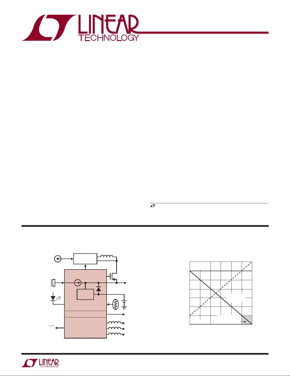
TYPICAL APPLICATION
HV SUPPLY
8V TO 38V
(TRANSIENTS
TO 60V)
USB OR
5V ADAPTER
CHARGE
RST
HIGH VOLTAGE
BUCK DC/DC
100mA/500mA
1000mA
CC/CV
CHARGER
LTC3557/LTC3557-1
ALWAYS ON LDO
TRIPLE HIGH EFFICIENCY
STEP-DOWN
SWITCHING REGULATORS
0V
NTC
35571 TA01a
V
OUT
+
SINGLE CELL
Li-Ion
3.3V/25mA
0.8V to 3.6V/600mA
0.8V to 3.6V/400mA
0.8V to 3.6V/400mA
Input and Battery Current vs Load Current
600
R
= 2k
PROG
R
CLPROG
500
400
300
200
CURRENT (mA)
100
0
WALL = 0V
–100
0
= 2k
100 200
I
IN
I
BAT
(CHARGING)
(DISCHARGING)
400 600
300 500
I
(mA)
LOAD
I
LOAD
I
BAT
35571 TA01b
35571fc
1
LTC3557/LTC3557-1
ABSOLUTE MAXIMUM RATINGS
(Notes 1-4)
V
, V
, V
BUS
OUT
IN1
, V
IN2
t < 1ms and Duty Cycle < 1% .................. −0.3V to 7V
Steady State ............................................. −0.3V to 6V
BAT, NTC, CHRG, WALL, V
,
C
MODE, FB1, FB2, FB3, RST2 ........................ −0.3V to 6V
EN1, EN2, EN3 .............................. −0.3V to V
ILIM0, ILIM1, PROG ....................... −0.3V to V
, I
, I
I
VBUS
VOUT
.....................................................................850mA
I
SW1
, I
I
SW2
SW3
, I
I
RST2
CHRG
I
CLPROG
, I
PROG
.........................................................2A
BAT
............................................................600mA
, I
.................................................75mA
ACPR
..........................................................2mA
OUT
CC
+ 0.3V
+ 0.3V
Maximum Operating Junction Temperature ..........110°C
Operating Ambient Temperature Range ... −40°C to 85°C
Storage Temperature Range ...................−65°C to 125°C
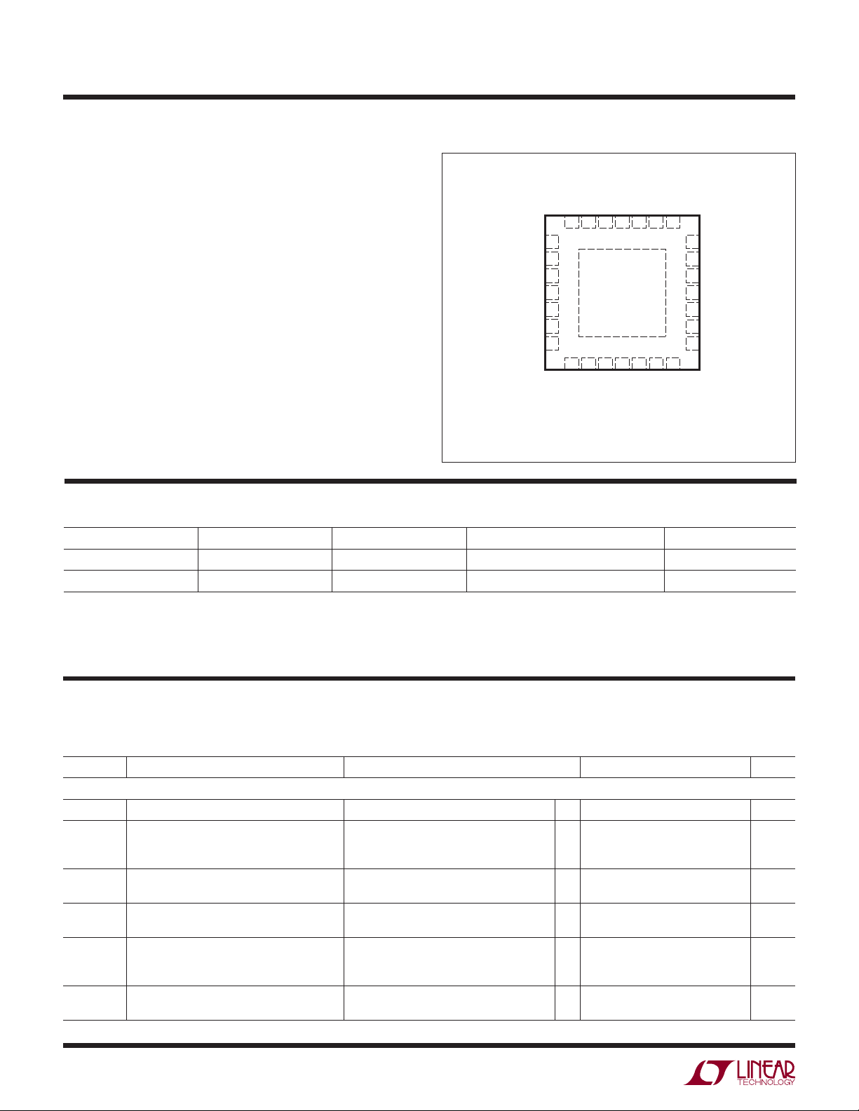
ORDER INFORMATION
PIN CONFIGURATION
TOP VIEW
CHRG
CLPROG
28 27 26 25 24 23
1
ILIM0
ILIM1
2
WALL
3
LDO3V3
4
SW1
5
V
6
IN1
FB1
7
8 9
10
EN1
MODE
28-LEAD (4mm s 4mm) PLASTIC QFN
EXPOSED PAD (PIN 29) IS GND, MUST BE SOLDERED TO PCB
UF PACKAGE
T
= 110°C, θJA = 37°C/W
JMAX
BUSVOUT
VCACPR
V
29
11 12 13 14
FB3
EN2
EN3
FB2
22
BAT
RST2
GATE
21
PROG
20
NTC
19
V
18
NTC
SW3
17
V
16
IN2
SW2
15
LEAD FREE FINISH TAPE AND REEL PART MARKING PACKAGE DESCRIPTION TEMPERATURE RANGE
LTC3557EUF#PBF LTC3557EUF#TRPBF 3557
LTC3557EUF-1#PBF LTC3557EUF-1#TRPBF 35571
Consult LTC Marketing for parts specifi ed with wider operating temperature ranges.
Consult LTC Marketing for information on non-standard lead based fi nish parts.
For more information on lead free part marking, go to: http://www.linear.com/leadfree/
For more information on tape and reel specifi cations, go to: http://www.linear.com/tapeandreel/
28-Lead (4mm × 4mm) Plastic QFN −40°C to 85°C
28-Lead (4mm × 4mm) Plastic QFN −40°C to 85°C
POWER MANAGER ELECTRICAL CHARACTERISTICS
The ● denotes the specifi cations which apply over the full operating temperature range, otherwise specifi cations are at TA = 25°C.
V
= 5V, V
BUS
SYMBOL PARAMETER CONDITIONS MIN TYP MAX UNITS
Input Power Supply
V
BUS
I
BUS(LIM)
I
BUSQ
h
CLPROG
V
CLPROG
V
UVLO
= 3.8V, ILIM0 = ILIM1 = 5V, WALL = EN1 = EN2 = EN3 = 0V, R
BAT
Input Supply Voltage 4.35 5.5 V
Total Input Current (Note 5) ILIM0 = 0V, ILIM1 = 0V (1x Mode)
Input Quiescent Current 1x, 5x, 10x Modes
Ratio of Measured V
Program Current
CLPROG Servo Voltage in Current Limit 1x Mode
V
Undervoltage Lockout Rising Threshold
BUS
Current to CLPROG
BUS
ILIM0 = 5V, ILIM1 = 5V (5x Mode)
ILIM0 = 5V, ILIM1 = 0V (10x Mode)
ILIM0 = 0V, ILIM1 = 5V (Suspend Mode)
1x, 5x, 10x Modes 1000 mA/mA
5x Mode
10x Mode
Falling Threshold
PROG
= 2k, R
CLPROG
●
●
= 2.1k.
80
450
900
3.5
90
475
950
0.35
0.05 0.1
0.2
1.0
2.0
3.8
3.7
100
500
1000
3.9 V
mA
mA
mA
mA
mA
35571fc
V
V
V
V
2
LTC3557/LTC3557-1
POWER MANAGER ELECTRICAL CHARACTERISTICS
The ● denotes the specifi cations which apply over the full operating temperature range, otherwise specifi cations are at TA = 25°C.
V
= 5V, V
BUS
SYMBOL PARAMETER CONDITIONS MIN TYP MAX UNITS
V
DUVLO
R
ON_LIM
Battery Charger
V
FLOAT
I
CHG
I
BAT
V
PROG
V
PROG(TRKL)
h
PROG
I
TRKL
V
TRKL
ΔV
RECHRG
t
TERM
t
BADBAT
End-of-Charge Indication Current Ratio (Note 6) 0.085 0.1 0.115 mA/mA
h
C/10
R
ON(CHG)
T
LIM
NTC
V
COLD
V
HOT
V
DIS
I
NTC
= 3.8V, ILIM0 = ILIM1 = 5V, WALL = EN1 = EN2 = EN3 = 0V, R
BAT
V
to V
BUS
Lockout
Differential Undervoltage
OUT
Rising Threshold
Falling Threshold
PROG
Input Current Limit Power FET
On-Resistance (Between V
V
Regulated Output Voltage LTC3557
BAT
BUS
and V
OUT
)
LTC3557, 0°C ≤ T
≤ 85°C
A
LTC3557-1
Constant Current Mode Charge Current R
Battery Drain Current V
LTC3557-1, 0°C ≤ T
= 1k, Input Current Limit = 2A
PROG
R
= 2k, Input Current Limit = 1A
PROG
R
= 5k, Input Current Limit = 400mA
PROG
> V
BUS
UVLO
V
= 0V, I
BUS
≤ 85°C
A
, Charger Off, I
= 0µA (Ideal Diode Mode)
OUT
OUT
PROG Pin Servo Voltage
PROG Pin Servo Voltage in Trickle Charge BAT < V
Ratio of I
to PROG Pin Current 1000 mA/mA
BAT
Trickle Charge Current BAT < V
Trickle Charge Rising Threshold
Trickle Charge Falling Threshold
TRKL
TRKL
BAT Rising
BAT Falling 2.5
Recharge Battery Threshold Voltage Threshold Voltage Relative to V
Safety Timer Termination Period Timer Starts when BAT = V
Bad Battery Termination Time BAT < V
TRKL
FLOAT
Battery Charger Power FET On-Resistance
(Between V
and BAT)
OUT
Junction Temperature in Constant
Temperature Mode
Cold Temperature Fault Threshold Voltage Rising NTC Voltage
Hysteresis
Hot Temperature Fault Threshold Voltage Falling NTC Voltage
Hysteresis
NTC Disable Threshold Voltage Falling NTC Voltage
Hysteresis
NTC Leakage Current NTC = V
BUS
= 5V
= 2k, R
CLPROG
= 2.1k.
50
100 mV
−50
0.2
= 0µA
4.179
4.165
4.079
4.065
●
950
●
465
●
180
4.200
4.200
4.100
4.100
1000
500
200
6
55
4.221
4.235
4.121
4.135
1050
535
220
27
100
1.000
0.100
40 50 60 mA
2.85
3.0 V
2.75
FLOAT
−75 −100 −115
– 50mV 3.2 4 4.8 Hour
0.4 0.5 0.6 Hour
200 m
110 °C
●
75 76
1.3
34 35
1.3
1.2 1.7
77 %V
%V
36 %V
%V
2.2 %V
VNTC
VNTC
VNTC
VNTC
VNTC
50
−50
50 nA
mV
mA
mA
mA
µA
µA
mV
mV
V
V
V
V
V
V
V
Ideal Diode
V
FWD
R
DROPOUT
I
MAX
Forward Voltage Detection I
Diode On-Resistance, Dropout I
Diode Current Limit (Note 7) 3.6 A
Always On 3.3V Supply
V
LDO3V3
R
OL(LDO3V3)
R
CL(LDO3V3)
Regulated Output Voltage 0mA < I
Open-Loop Output Resistance BAT = 3.0V, V
Closed-Loop Output Resistance 3.2
= 10mA 5 15 25 mV
OUT
= 1A 200 m
OUT
< 25mA 3.1 3.3 3.5 V
LDO3V3
= 0V 24
BUS
35571fc
3
LTC3557/LTC3557-1
POWER MANAGER ELECTRICAL CHARACTERISTICS
The ● denotes the specifi cations which apply over the full operating temperature range, otherwise specifi cations are at TA = 25°C.
V
= 5V, V
BUS
SYMBOL PARAMETER CONDITIONS MIN TYP MAX UNITS
Wall Adapter
V
ACPR
V
W
ΔV
W
I
QWALL
Logic (I
LIM0
V
IL
V
IH
I
PD
V
CHRG
I
CHRG
= 3.8V, ILIM0 = ILIM1 = 5V, WALL = EN1 = EN2 = EN3 = 0V, R
BAT
ACPR Pin Output High Voltage
ACPR Pin Output Low Voltage
I
ACPR
I
ACPR
= 1mA
= 1mA
Absolute Wall Input Threshold Voltage WALL Rising
WALL Falling 3.1
Differential Wall Input Threshold Voltage
WALL − BAT Falling
WALL − BAT Rising
Wall Operating Quiescent Current
, I
and CHRG)
LIM1
I
+ I
WALL
WALL = V
VOUT
OUT
, I
= 5V
BAT
= 0mA,
PROG
= 2k, R
CLPROG
= 2.1k.
V
− 0.3
OUT
025
V
440 µA
OUT
0 0.3
4.3
4.45 V
3.2
75 150
Input Low Voltage ILIM0, ILIM1 0.4 V
Input High Voltage ILIM0, ILIM1 1.2 V
Static Pull-Down Current ILIM0, ILIM1; V
CHRG Pin Output Low Voltage I
= 10mA 0.15 0.4 V
CHRG
= 1V 2 µA
PIN
CHRG Pin Input Current BAT = 4.5V, CHRG = 5V 0 1 µA
mV
mV
V
V
V
SWITCHING REGULATOR ELECTRICAL CHARACTERISTICS
The ● denotes the specifi cations which apply over the full operating temperature range, otherwise specifi cations are at TA = 25°C.
V
= V
= V
OUT
IN1
SYMBOL PARAMETER CONDITIONS MIN TYP MAX UNITS
Step-Down Switching Regulators 1, 2 and 3
, V
V
IN1
IN2
V
UVL0 V
OUT
f
OSC
V
IL
V
IH
I
PD
Step-Down Switching Regulator 1
I
VIN1
I
LIM1
V
FB1
I
FB1
D1 Maximum Duty Cycle FB1 = 0V, EN1 = 3.8V 100 %
R
P1
R
N1
R
SW1(PD)
= 3.8V, MODE = EN1 = EN2 = EN3 = 0V.
IN2
Input Supply Voltage (Note 9)
V
OUT
OUT
Falling
Rising
and V
V
IN1
Impedance. Switching Regulators are Disabled
Below V
Connected to V
IN2
UVLO
OUT
Through Low
OUT
●
2.7 5.5 V
2.5 2.7
2.8 2.9
Oscillator Frequency 1.91 2.25 2.59 MHz
Input Low Voltage MODE, EN1, EN2, EN3 0.4 V
Input High Voltage MODE, EN1, EN2, EN3 1.2 V
Static Pull-Down Current MODE, EN1, EN2, EN3 (V
Pulse-Skip Mode Input Current (Note 10) I
Burst Mode Input Current (Note 10) I
Shutdown Input Current I
= 0, EN1 = 3.8V, MODE = 0V 220 µA
OUT
= 0, EN1 = MODE = 3.8V 35 50 µA
OUT
= 0, EN1 = 0V, FB1 = 0V 0.01 1 µA
OUT
= 1V) 1 µA
PIN
Peak PMOS Current Limit EN1 = 3.8V, MODE = 0V or 3.8V (Note 7) 900 1200 1500 mA
Feedback Voltage EN1 = 3.8V, MODE = 0V
EN1 = MODE = 3.8V
FB1 Input Current (Note 10) EN1 = 3.8V
R
of PMOS EN1 = 3.8V 0.3
DS(ON)
R
of NMOS EN1 = 3.8V 0.4
DS(ON)
●
0.78
●
0.78
−0.05
0.8
0.8
0.82
0.824
0.05 µA
SW1 Pull-Down in Shutdown EN1 = 0V 10 k
V
V
V
V
4
35571fc
LTC3557/LTC3557-1
SWITCHING REGULATOR ELECTRICAL CHARACTERISTICS
The ● denotes the specifi cations which apply over the full operating temperature range, otherwise specifi cations are at TA = 25°C.
V
= V
= V
OUT
IN1
SYMBOL PARAMETER CONDITIONS MIN TYP MAX UNITS
Step-Down Switching Regulator 2
I
VIN2
I
LIM2
V
FB2
I
FB2
D2 Maximum Duty Cycle FB2 = 0V, EN2 = 3.8V 100 %
R
P2
R
N2
R
SW2(PD)
V
RST2
I
RST2
V
TH(RST2)
t
RST2
Step-Down Switching Regulator 3
I
VIN2
I
LIM3
V
FB3
I
FB3
D3 Maximum Duty Cycle FB3 = 0V, EN3 = 3.8V 100 %
R
P3
R
N3
R
SW3(PD)
= 3.8V, MODE = EN1 = EN2 = EN3 = 0V.
IN2
Pulse-Skip Mode Input Current (Note 10) I
Burst Mode Input Current (Note 10) I
Shutdown Input Current I
= 0, EN2 = 3.8V, MODE = 0V 220 µA
OUT
= 0, EN2 = MODE = 3.8V 35 50 µA
OUT
= 0, EN2 = 0V, FB2 = 0V 0.01 1 µA
OUT
Peak PMOS Current Limit EN2 = 3.8V, MODE = 0V or 3.8V (Note 7) 600 800 1000 mA
Feedback Voltage EN2 = 3.8V, MODE = 0V
EN2 = MODE = 3.8V
FB2 Input Current (Note 10) EN2 = 3.8V
R
of PMOS EN2 = 3.8V 0.6
DS(ON)
R
of NMOS EN2 = 3.8V 0.6
DS(0N)
SW2 Pull-Down in Shutdown EN2 = 0V 10
Power-On RST2 Pin Output Low Voltage I
Power-On RST2 Pin Input Current (Note 10) V
= 1mA, FB2 = 0V, EN2 = 3.8V 0.1 0.35 V
RST2
= 5.5V, EN2 = 3.8V 1 µA
RST2
Power-On RST2 Pin Threshold (Note 8)
●
0.78
●
0.78
−0.05
0.8
0.8
0.82
0.824
0.05 µA
kΩ
−8
Power-On RST2 Pin Delay From RST2 Threshold to RST2 Hi-Z 230 ms
Pulse-Skip Mode Input Current (Note 10) I
Burst Mode Input Current (Note 10) I
Shutdown Input current I
= 0, EN3 = 3.8V, MODE = 0V 220 µA
OUT
= 0, EN3 = MODE = 3.8V 35 50 µA
OUT
= 0, EN3 = 0V, FB3 = 0V 0.01 1 µA
OUT
Peak PMOS Current Limt EN3 = 3.8V, MODE = 0V or 3.8V (Note 7) 600 800 1000 mA
Feedback Voltage EN3 = 3.8V, MODE = 0V
EN3 = MODE = 3.8V
FB3 Input Current (Note 10) EN3 = 3.8V
R
of PMOS EN3 = 3.8V 0.6
DS(ON)
R
of NMOS EN3 = 3.8V 0.6
DS(ON)
●
0.78
●
0.78
−0.05
0.8
0.8
0.82
0.824
0.05 µA
SW3 Pull-Down in Shutdown EN3 = 0V 10 k
V
V
Ω
Ω
%
V
V
Note 1. Stresses beyond those listed under Absolute Maximum Ratings
may cause permanent damage to the device. Exposure to any Absolute
Maximum Rating condition for extended periods may affect device
reliability and lifetime.
Note 2. The LTC3557/LTC3557-1 is guaranteed to meet performance
specifi cations from 0°C to 85°C. Specifi cations over the −40°C to 85°C
operating temperature range are assured by design, characterization and
correlation with statistical process controls.
Note 3. This IC includes overtemperature protection that is intended
to protect the device during momentary overload conditions. Junction
temperatures will exceed 110°C when overtemperature protection is
active. Continuous operation above the specifi ed maximum operating
junction temperature may result in device degradation or failure.
Note 4. V
is the greater of V
CC
BUS
, V
OUT
or BAT.
Note 5. Total input current is the sum of quiescent current, I
measured current given by V
Note 6. h
is expressed as a fraction of measured full charge current
C/10
CLPROG/RCLPROG
• (h
CLPROG
+ 1)
BUSQ
, and
with indicated PROG resistor.
Note 7. The current limit features of this part are intended to protect the
IC from short term or intermittent fault conditions. Continuous operation
above the maximum specifi ed pin current rating may result in device
degradation or failure.
Note 8. RST2 threshold is expressed as a percentage difference from the
FB2 regulation voltage. The threshold is measured for FB2 rising.
Note 9. V
not in UVLO.
OUT
Note 10. FB high, not switching.
35571fc
5
LTC3557/LTC3557-1
TYPICAL PERFORMANCE CHARACTERISTICS
= 25°C unless otherwise specifi ed
T
A
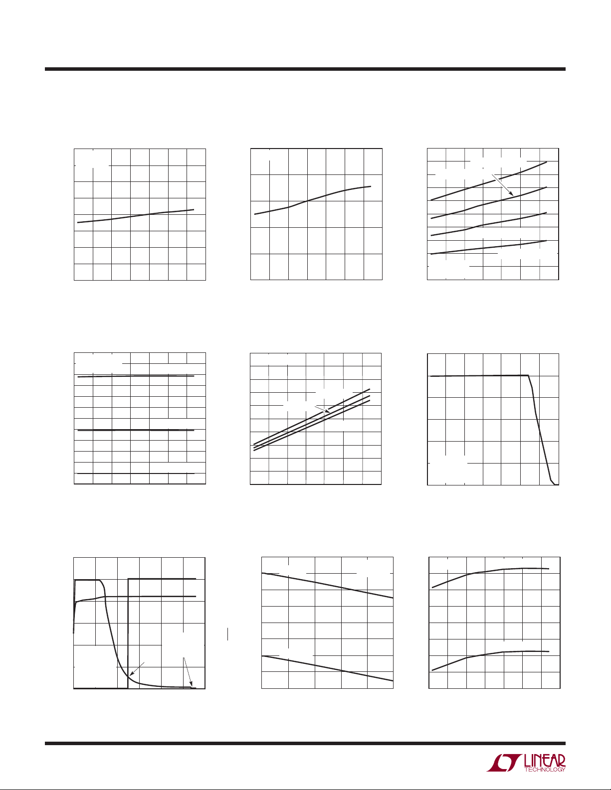
Input Supply Current
vs Temperature
0.8
V
= 5V
BUS
1x MODE
0.7
0.6
0.5
(mA)
0.4
VBUS
I
0.3
0.2
0.1
0
–25 0 50
–50
TEMPERATURE (°C)
Input Current Limit
vs Temperature
1200
V
= 5V
BUS
1100
1000
900
800
700
(mA)
600
500
VBUS
I
400
300
200
100
0
–50
R
CLPROG
–25
= 2.1k
0
TEMPERATURE (°C)
Input Supply Current
vs Temperature (Suspend Mode)
0.10
V
= 5V
BUS
0.08
0.06
(mA)
VBUS
0.04
I
0.02
0
25
75 100 125
35571 G01
–50 –25
0
TEMPERATURE (°C)
50
25
75
100
125
35571 G02
Battery Drain Current
vs Temperature
0.20
0.18
2 BUCKS ENABLED
0.16
0.14
0.12
(mA)
0.10
BAT
I
0.08
0.06
0.04
V
BAT
MODE = 3.8V
0
–50
= 3.8V
–25
0
TEMPERATURE (°C)
0.02
3 BUCKS ENABLED
1 BUCK ENABLED
N0 BUCKS ENABLED
50
25
100
125
35571 G03
75
Charge Current vs Temperature
Input RON vs Temperature
300
I
= 400mA
OUT
10x MODE
5x MODE
1x MODE
50
25
75
100
125
35571 G04
280
260
240
220
180
(m)
ON
R
160
140
120
100
V
= 4.5V
BUS
V
= 5V
BUS
V
= 5.5V
BUS
0
–50
0
–25
TEMPERATURE (°C)
50
25
75
100
125
35571 G05
(Thermal Regulation)
600
500
400
(mA)
300
BAT
I
200
V
= 5V
BUS
100
10x MODE
= 2k
R
PROG
0
–50
–25 0
TEMPERATURE (°C)
50 100 125
25 75
35571 G06
Battery Current and Voltage
vs Time (LTC3557)
600
500
400
(mA)
300
BAT
I
200
1450mAhr
CELL
= 5V
V
100
BUS
= 2k
R
PROG
= 2k
R
CLPROG
0
0
234
1
6
C/10
TIME (HOUR)
CHRG
V
BAT
SAFETY
TIMER
TERMINATION
I
BAT
56
35571 G07
Battery Regulation (Float)
V
Load Regulation
6
5
V
BAT
4
AND V
3
CHRG
(V)
2
1
0
4.22
4.20
4.18
4.16
(V)
4.14
FLOAT
V
4.12
4.10
4.08
4.06
FLOAT
LTC3557
LTC3557-1
200 400 800
0
I
BAT
(mA)
600
V
= 5V
BUS
10x MODE
35571 G08
1000
Voltage vs Temperature
4.22
I
= 2mA
BAT
4.20
4.18
4.16
(V)
4.14
FLOAT
V
4.12
4.10
4.08
4.06
–50
–25
0
TEMPERATURE (°C)
25
LTC3557
LTC3557-1
50
75
100
125
35571 G09
35571fc
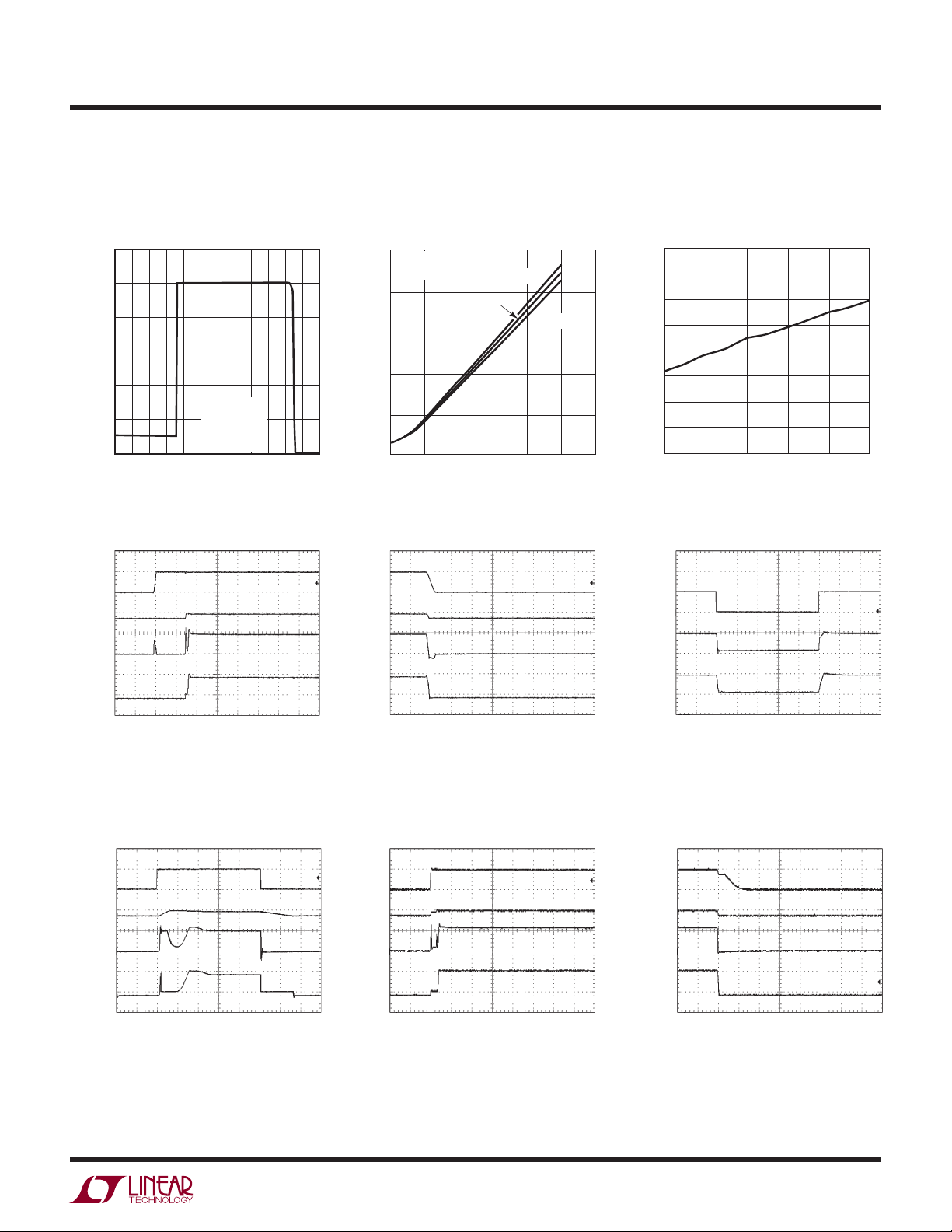
TYPICAL PERFORMANCE CHARACTERISTICS
Forward Voltage vs Ideal Diode
I
600
500
400
(mA)
300
BAT
I
200
100
vs V
BAT
0
2.0
BAT
2.8 3.2 3.6
2.4
V
BUS
10x MODE
R
PROG
R
CLPROG
V
(V)
BAT
= 5V
= 2k
= 2k
4.0 4.4
35571 G10
Current (No External FET)
0.25
V
= 0V
BUS
= 25°C
T
A
(V)
FWD
V
0.20
0.15
0.10
0.05
0
0
V
BAT
0.4 0.6 0.8
0.2
= 3.6V
I
BAT
V
(A)
BAT
= 3.2V
V
BAT
LTC3557/LTC3557-1
T
= 25°C unless otherwise specifi ed
A
Forward Voltage
vs Ideal Diode Current
(with Si2333DS External FET)
40
V
= 3.8V
BAT
= 0V
V
BUS
35
= 25°C
T
A
30
= 4.2V
1.0 1.2
35571 G11
(mV)
FWD
V
25
20
15
10
5
0
0.2 0.4 0.8
0
0.6
I
(A)
BAT
1.0
35571 G12
Input Connect Waveform
V
BUS
5V/DIV
V
OUT
5V/DIV
I
BUS
0.5A/DIV
I
BAT
0.5A/DIV
V
BAT
I
OUT
R
CLPROG
R
PROG
= 3.75V
= 100mA
= 2k
1ms/DIV
= 2k
Switching from Suspend Mode
to 5x Mode
ILIM0
5V/DIV
V
OUT
5V/DIV
I
BUS
0.5A/DIV
I
BAT
0.5A/DIV
35571 G25
Input Disconnect Waveform
V
BUS
5V/DIV
V
OUT
5V/DIV
I
BUS
0.5A/DIV
I
BAT
0.5A/DIV
V
= 3.75V
BAT
= 100mA
I
OUT
= 2k
R
CLPROG
= 2k
R
PROG
WALL Connect Waveform
WALL
5V/DIV
V
OUT
5V/DIV
I
WALL
0.5A/DIV
I
BAT
0.5A/DIV
1ms/DIV
35571 G26
ILIM0/ILIM1
5V/DIV
I
BUS
0.5A/DIV
I
BAT
0.5A/DIV
WALL
5V/DIV
V
OUT
5V/DIV
I
WALL
0.5A/DIV
I
0.5A/DIV
Switching from 1x to 5x Mode
V
BAT
I
OUT
R
CLPROG
R
PROG
= 3.75V
= 50mA
= 2k
1ms/DIV
= 2k
WALL Disconnect Waveform
BAT
35571 G27
V
= 3.75V
BAT
= 100mA
I
OUT
R
CLPROG
= 2k
R
PROG
ILIM1 = 5V
= 2k
100µs/DIV
35571 G28
V
I
R
BAT
OUT
PROG
= 3.75V
= 100mA
= 2k
1ms/DIV
35571 G29
V
I
R
BAT
OUT
PROG
= 3.75V
= 100mA
= 2k
1ms/DIV
35571 G30
35571fc
7
LTC3557/LTC3557-1
0
0
0
5
TYPICAL PERFORMANCE CHARACTERISTICS
Oscillator Frequency
vs Temperature
2.5
2.4
2.3
2.2
2.1
2.0
(MHz)
OSC
1.9
f
1.8
1.7
1.6
1.5
–50
–25
VIN = 2.9V
50
25
0
TEMPERATURE (°C)
Step-Down Switching Regulator 3
1.8V Output Effi ciency vs I
100
90
Burst Mode
80
OPERATION
70
60
50
40
EFFICIENCY (%)
30
20
10
0
0.01
0.1 1 10 100 100
I
OUT3
PULSE SKIP
(mA)
VIN = 3.8V
VIN = 5V
VIN = 2.7V
75
OUT3
V
OUT3
V
IN3
V
IN3
100
35571 G13
= 1.8V
= 3.8V
= 5V
35571 G16
125
Step-Down Switching Regulator 1
3.3V Output Effi ciency vs I
100
Burst Mode
90
OPERATION
80
70
60
50
40
EFFICIENCY (%)
30
20
10
0
0.01
0.1 1 10 100 100
I
OUT1
PULSE SKIP
(mA)
Step-Down Switching Regulator
Pulse Skip Supply Current vs V
400
V
= 1.2V
OUTX
= 0mA
I
OUTX
350
300
250
(µA)
IN
I
200
150
100
2.5
3.0 3.5 4.0 4.5
V
(V)
INX
V
OUT1
V
V
TA = 25°C unless otherwise specifi ed
Step-Down Switching Regulator 2
OUT1
= 3.3V
= 3.8V
IN1
= 5V
IN1
35571 G14
1.2V Output Effi ciency vs I
100
90
Burst Mode
80
OPERATION
70
60
50
40
EFFICIENCY (%)
30
20
10
0
0.01
0.1 1 10 100 100
Step-Down Switching
Regulator Short-Circuit Current
INX
110°C
75°C
25°C
–45°C
5.0
vs Temperature
1200
1100
1000
900
800
700
600
SHORT-CIRCUIT CURRENT (mA)
500
400
–25 0 50
–50
TEMPERATURE (°C)
PULSE SKIP
I
(mA)
OUT2
600mA BUCK
400mA BUCK
25
OUT2
V
= 1.2V
OUT2
V
= 3.8V
IN2
= 5V
V
IN2
35571 G15
75 100 125
35571 G18
50mV/DIV
50mV/DIV
I
OUT2
8
Step-Down Switching Regulator
Output Transient (MODE = 1)
V
OUT2
(AC)
V
OUT3
(AC)
300mA
5mA
V
I
OUT3
OUT2
OUT3
= 1.2V
= 1.8V
= 16mA
50µs/DIVV
35571 G1
50mV/DIV
50mV/DIV
I
OUT2
Step-Down Switching Regulator
Output Transient (MODE = 0)
V
OUT2
(AC)
V
OUT3
(AC)
300mA
5mA
V
I
OUT3
OUT2
OUT3
= 1.2V
= 1.8V
= 100mA
50µs/DIVV
0.9
0.8
0.7
0.6
0.5
0.4
0.3
SWITCH IMPEDANCE ()
35571 G2
0.2
0.1
Step-Down Switching Regulator
Switch Impedance vs Temperature
V
= 3.2V
INX
400mA
400mA
NMOS
0
–50
–25
PMOS
600mA NMOS
0
25 12
TEMPERATURE (°C)
50
600mA PMOS
75 100
35571 G21
35571fc
LTC3557/LTC3557-1
4
TYPICAL PERFORMANCE CHARACTERISTICS
600mA Step-Down Switching
Regulator Feedback Voltage
vs Output Current
0.85
0.84
0.83
0.82
0.81
0.80
0.79
FEEDBACK (V)
0.78
0.77
0.76
0.75
0.1 10 100 1000
Burst Mode
OPERATION
PULSE SKIP
1
OUTPUT CURRENT (mA)
3.8V
5V
35571 G22
400mA Step-Down Switching
Regulator Feedback Voltage
vs Output Current
0.85
0.84
0.83
0.82
0.81
0.80
0.79
FEEDBACK (V)
0.78
0.77
0.76
0.75
0.1 10 100 1000
Burst Mode
OPERATION
PULSE SKIP
1
OUTPUT CURRENT (mA)
PIN FUNCTIONS
TA = 25°C unless otherwise specifi ed
Step-Down Switching Regulator
Start-Up Waveform
V
OUT2
50mV/DIV(AC)
V
OUT1
1V/DIV
0V
I
L1
200mA/DIV
0mA
EN1
3.8V
5V
35571 G23
= 1.2V
OUT2
= 50mA
I
OUT2
MODE = 1
= 8
R
OUT1
100µs/DIVV
35571 G2
ILIM0, ILIM1 (Pins 1, 2): Input Current Control Pins. ILIM0
and ILIM1 control the input current limit. See Table 1. Both
pins are pulled low by a weak current sink.
WALL (Pin 3): Wall Adapter Present Input. Pulling this pin
above 4.3V will disconnect the power path from V
. The ACPR pin will also be pulled low to indicate that a
V
OUT
BUS
to
wall adapter has been detected.
LDO3V3 (Pin 4): Always On 3.3V LDO Output. The
LDO3V3 pin provides a regulated, always-on 3.3V supply
voltage. This pin gets its power from V
. It may be used
OUT
for light loads such as a real-time clock or housekeeping
microprocessor. A 1µF capacitor is required from LDO3V3
to ground if it will be called upon to deliver current. If
the LDO3V3 output is not used it should be disabled by
connecting it to V
OUT
.
SW1 (Pin 5): Power Transmission (Switch) Pin for
Step-Down Switching Regulator 1.
(Pin 6): Power Input for Step-Down Switching
V
IN1
Regulator 1. This pin will generally be connected to V
OUT
.
FB1 (Pin 7): Feedback Input for Step-Down Switching
Regulator 1. This pin servos to a fi xed voltage of 0.8V when
the control loop is complete.
MODE (Pin 8): Low Power Mode Enable. When this pin is
pulled high, the three step-down switching regulators are
set to low power Burst Mode operation.
EN1 (Pin 9): Logic Input Enables Step-Down Switching
Regulator 1.
EN2 (Pin 10): Logic Input Enables Step-Down Switching
Regulator 2.
EN3 (Pin 11): Logic Input Enables Step-Down Switching
Regulator 3.
FB3 (Pin 12): Feedback Input for Step-Down Switching
Regulator 3. This pin servos to a fi xed voltage of 0.8V when
the control loop is complete.
FB2 (Pin 13): Feedback Input for Step-Down Switching
Regulator 2. This pin servos to a fi xed voltage of 0.8V when
the control loop is complete.
RST2 (Pin 14): This is an open-drain output which indicates
that step-down switching regulator 2 has settled to its fi nal
value. It can be used as a power on reset for the primary
microprocessor or to enable the other buck regulators for
supply sequencing.
SW2 (Pin 15): Power Transmission (Switch) Pin for
Step-Down Switching Regulator 2.
35571fc
9

LTC3557/LTC3557-1
PIN FUNCTIONS
V
(Pin 16): Power Input for Step-Down Switching Regu-
IN2
lators 2 and 3. This pin will generally be connected to V
SW3 (Pin 17): Power Transmission (Switch) Pin for
Step-Down Switching Regulator 3.
(Pin 18): Output Bias Voltage for NTC. A resistor from
V
NTC
this pin to the NTC pin will bias the NTC thermistor.
NTC (Pin 19): The NTC pin connects to a battery’s thermistor
to determine if the battery is too hot or too cold to charge. If
the battery’s temperature is out of range, charging is paused
until it drops back into range. A low drift bias resistor is
required from V
to NTC and a thermistor is required from
NTC
NTC to ground. If the NTC function is not desired, the NTC
pin should be grounded.
PROG (Pin 20): Charge Current Program and Charge
Current Monitor Pin. Connecting a resistor from PROG to
ground programs the charge current:
(A)=
1000V
R
PROG
I
CHG
If suffi cient input power is available in constant current
mode, this pin servos to 1V. The voltage on this pin always
represents the actual charge current.
GATE (Pin 21): Ideal Diode Gate Connection. This pin
controls the gate of an optional external P-channel MOSFET
transistor used to supplement the internal ideal diode. The
source of the P-channel MOSFET should be connected
to V
and the drain should be connected to BAT. It is
OUT
important to maintain high impedance on this pin and
minimize all leakage paths.
BAT (Pin 22): Single Cell Li-Ion Battery Pin. Depending on
available power and load, a Li-Ion battery on BAT will either
deliver system power to V
through the ideal diode or be
OUT
charged from the battery charger.
(Pin 23): Output Voltage of the PowerPath Controller
V
OUT
and Input Voltage of the Battery Charger. The majority of
the portable product should be powered from V
OUT
LTC3557/LTC3557-1 will partition the available power
between the external load on V
and the internal battery
OUT
charger. Priority is given to the external load and any extra
power is used to charge the battery. An ideal diode from
BAT to V
ensures that V
OUT
is powered even if the load
OUT
.
OUT
. The
exceeds the allotted input current from V
power source is removed. V
should be bypassed with
OUT
BUS
or if the V
BUS
a low impedance multilayer ceramic capacitor. The total
capacitance on V
should maintain a minimum of 5µF
OUT
over operating voltage and temperature.
(Pin 24): USB Input Voltage. V
V
BUS
will usually be
BUS
connected to the USB port of a computer or a DC output wall
adapter. V
should be bypassed with a low impedance
BUS
multilayer ceramic capacitor.
ACPR (Pin 25): Wall Adapter Present Output (Active
Low). A low on this pin indicates that the wall adapter
input comparator has had its input pulled above its input
threshold (typically 4.3V). This pin can be used to drive the
gate of an external P-channel MOSFET to provide power to
from a power source other than a USB port.
V
OUT
(Pin 26): High Voltage Buck Regulator Control Pin. This
V
C
pin can be used to drive the V
pin of an approved external
C
high voltage buck switching regulator. An external P-channel
MOSFET is required to provide power to V
tied to the ACPR pin. The V
®
3480, LT3481 and LT3505.
LT
pin is designed to work with the
C
with its gate
OUT
CLPROG (Pin 27): Input Current Program and Input Current
Monitor Pin. A resistor from CLPROG to ground determines
the upper limit of the current drawn from the V
BUS
pin
(i.e., the input current limit). A precise fraction of the input
current, h
CLPROG
, is sent to the CLPROG pin. The input
PowerPath delivers current until the CLPROG pin reaches
2.0V (10x Mode), 1.0V (5x Mode) or 0.2V (1x Mode).
Therefore, the current drawn from V
amount given by h
the resistor R
CLPROG
CLPROG
and R
CLPROG
should be set to no less than 2.1k.
will be limited to an
BUS
. In USB applications
CHRG (Pin 28): Open-Drain Charge Status Output. The
CHRG pin indicates the status of the battery charger.
Four possible states are represented by CHRG: charging,
not charging (i.e., fl oat charge current less than 1/10th
programmed charge current), unresponsive battery (i.e., its
voltage remains below 2.8V after 1/2 hour of charging) and
battery temperature out of range. CHRG requires a pull-up
resistor and/or LED to provide indication.
Exposed Pad (Pin 29): Ground. The exposed package pad
is ground and must be soldered to the PC board for proper
functionality and for maximum heat transfer.
35571fc
10

BLOCK DIAGRAM
LTC3557/LTC3557-1
24
27
18
19
28
1
2
V
BUS
CLPROG
V
NTC
NTC
CHRG
ILIM0
ILIM1
DETECT
BATTERY
TEMP
MONITOR
CHARGE
STATUS
ILIM
LOGIC
3
WALL
WALL
INPUT
CURRENT
LIMIT
CC/CV
CHARGER
REF
25
ACPR
IDEAL
DIODE
OSC
EN
MODE
OSC
26
V
V
C
CONTROL
+
–
–
+
15mV
600mA, 2.25MHz
BUCK REGULATOR
400mA, 2.25MHz
BUCK REGULATOR
C
V
OUT
23
GATE
21
BAT
22
PROG
20
3.3V
LDO
LDO3V3
V
SW1
FB1
V
IN1
IN2
4
6
5
7
16
EN1
9
EN2
10
EN3
11
MODE
8
RST2
14
EN
LOGIC
GND
29
EN
MODE
400mA, 2.25MHz
BUCK REGULATOR
OSC
EN
MODE
SW2
FB2
SW3
FB3
15
13
17
12
35571 BD
35571fc
11

LTC3557/LTC3557-1
OPERATION
Introduction
The LTC3557/LTC3557-1 is a highly integrated power
management IC that includes a PowerPath controller,
battery charger, an ideal diode, an always-on LDO, three
synchronous step-down switching regulators as well as
a buck regulator V
controller. Designed specifi cally for
C
USB applications, the PowerPath controller incorporates
a precision input current limit which communicates with
the battery charger to ensure that input current never
violates the USB specifi cations.
The ideal diode from BAT to V
power is always available to V
or absent power at V
BUS
.
guarantees that ample
OUT
even if there is insuffi cient
OUT
The LTC3557/LTC3557-1 also has the ability to receive
power from a wall adapter or other non-current-limited
power source. Such a power supply can be connected
to the V
pin of the LTC3557/LTC3557-1 through an
OUT
external device such as a power Schottky or FET as shown
in Figure 1.
The LTC3557/LTC3557-1 has the unique ability to use
the output, which is powered by an external supply, to
charge the battery while providing power to the load. A
comparator on the WALL pin is confi gured to detect the
presence of the wall adapter and shut off the connection
to the USB. This prevents reverse conduction from V
to V
The LTC3557/LTC3557-1 provides a V
can be used to drive the V
when a wall adapter is present.
BUS
pin of an external high voltage
C
output pin which
C
OUT
buck switching regulator such as the LT3480, LT3481, or
LT3505 to provide power to the V
pin. The VC control
OUT
circuitry adjusts the regulation point of the switching
regulator to a small voltage above the BAT pin voltage.
This control method provides a high input voltage, high
effi ciency battery charger and PowerPath function.
An “always on” LDO provides a regulated 3.3V from V
OUT
.
This LDO will be on at all times and can be used to supply
up to 25mA.
FROM AC ADAPTER (OR HIGH VOLTAGE BUCK OUTPUT)
4.3V
3.2V
–
+
(RISING)
(FALLING)
WALL
3
+
–
75mV (RISING)
+
–
25mV (FALLING)
FROM
USB
V
BUS
24
26
V
C
OPTIONAL CONTROL
FOR HIGH VOLTAGE BUCK REGS
LT3480, LT3481 OR LT3505
ENABLE
USB CURRENT LIMIT
CONSTANT CURRENT
CONSTANT VOLTAGE
BATTERY CHARGER
V
OUT
BAT
IDEAL
DIODE
ACPR
25
V
OUT
23
+
GATE
BAT
35571 F01
21
22
+
–
–
+
15mV
SYSTEM
LOAD
OPTIONAL
EXTERNAL
IDEAL DIODE
PMOS
Li-Ion
12
Figure 1. Simplifi ed PowerPath Block Diagram
35571fc

OPERATION
LTC3557/LTC3557-1
The LTC3557/LTC3557-1 includes three 2.25MHz constant
frequency current mode step-down switching regulators
providing 400mA, 400mA and 600mA each. All stepdown switching regulators can be programmed for a
minimum output voltage of 0.8V and can be used to power
a microcontroller core, microcontroller I/O, memory or
other logic circuitry. All step-down switching regulators
support 100% duty cycle operation and are capable of
operating in Burst Mode operation for highest effi ciencies
at light loads (Burst Mode operation is pin selectable). No
external compensation components are required for the
switching regulators.
USB PowerPath Controller
The input current limit and charge control circuits of the
LTC3557/LTC3557-1 are designed to limit input current
as well as control battery charge current as a function of
. V
I
VOUT
drives the combination of the external load,
OUT
the three step-down switching regulators, always on 3.3V
LDO and the battery charger.
If the combined load does not exceed the programmed
input current limit, V
will be connected to V
OUT
through
BUS
an internal 200m P-channel MOSFET.
If the combined load at V
exceeds the programmed
OUT
input current limit, the battery charger will reduce its charge
current by the amount necessary to enable the external
load to be satisfi ed while maintaining the programmed
input current. Even if the battery charge current is set to
exceed the allowable USB current, the average input current
USB specifi cation will not be violated. Furthermore, load
current at V
will always be prioritized and only excess
OUT
available current will be used to charge the battery.
The input current limit is programmed by the ILIM0 and
ILIM1 pins. The LTC3557/LTC3557-1 can be confi gured to
limit input current to one of several possible settings as well
as be deactivated (USB Suspend). The input current limit
will be set by the appropriate servo voltage and the resistor
on CLPROG according to the following expression:
I
= I
VBUS
I
VBUS
I
VBUS
= I
= I
BUSQ
BUSQ
BUSQ
+
+
+
0.2V
R
CLPROG
1V
R
CLPROG
2V
R
CLPROG
•h
CLPROG
•h
CLPROG
•h
CLPROG
1x Mode
()
5x Mode
()
10x Mode
()
Under worst-case conditions, the USB specifi cation will not
be violated with an R
CLPROG
resistor of greater than 2.1k.
Table 1 shows the available settings for the ILIM0 and
ILIM1 pins:
Table 1: Controlled Input Current Limit
ILIM1 ILIM0 I
0 0 100mA (1x)
0 1 1A (10x)
1 0 Suspend
1 1 500mA (5x)
BUS(LIM)
Notice that when ILIM0 is high and ILIM1 is low, the input
current limit is set to a higher current limit for increased
charging and current availability at V
. This mode is
OUT
typically used when there is power available from a wall
adapter.
The current out of the CLPROG pin is a fraction (1/h
of the V
current. When a programming resistor is con-
BUS
CLPROG
)
nected from CLPROG to GND, the voltage on CLPROG
represents the input current:
V
I
VBUS
where I
= I
BUSQ
BUSQ
and h
+
R
CLPROG
CLPROG
CLPROG
•h
CLPROG
are given in the Electrical
Characteristics.
Ideal Diode from BAT to V
OUT
The LTC3557/LTC3557-1 has an internal ideal diode as well
as a controller for an optional external ideal diode. Both
the internal and the external ideal diodes respond quickly
whenever V
drops below BAT.
OUT
If the load increases beyond the input current limit, additional current will be pulled from the battery via the
ideal diodes. Furthermore, if power to V
(external wall power or high voltage regulator) is
V
OUT
(USB) or
BUS
removed, then all of the application power will be provided
35571fc
13

LTC3557/LTC3557-1
OPERATION
by the battery via the ideal diodes. The ideal diodes are
fast enough to keep V
from dropping with just the
OUT
recommended output capacitor. The ideal diode consists
of a precision amplifi er that enables an on-chip P-channel
MOSFET whenever the voltage at V
15mV (V
) below the voltage at BAT. The resistance of
FWD
is approximately
OUT
the internal ideal diode is approximately 200m. If this is
suffi cient for the application, then no external components
are necessary. However, if more conductance is needed,
an external P-channel MOSFET can be added from BAT
OUT
.
to V
The GATE pin of the LTC3557/LTC3557-1 drives the gate of
the external P-channel MOSFET for automatic ideal diode
control. The source of the MOSFET should be connected
to V
and the drain should be connected to BAT. Capable
OUT
of driving a 1nF load, the GATE pin can control an external
P-channel MOSFET having extremely low on-resistance.
Using the WALL Pin to Detect the Presence of an
External Power Source
The WALL input pin can be used to identify the presence
of an external power source (particularly one that is not
subject to a fi xed current limit like the USB V
BUS
input).
Typically, such a power supply would be a 5V wall adapter
output or the low voltage output of a high voltage buck
regulator (specifi cally, LT3480, LT3481 or LT3505). When
the wall adapter output (or buck regulator output) is connected directly to the WALL pin, and the voltage exceeds
the WALL pin threshold, the USB power path (from V
to V
) will be disconnected. Furthermore, the ACPR pin
OUT
BUS
will be pulled low. In order for the presence of an external
power supply to be acknowledged, both of the following
conditions must be satisfi ed:
1. The WALL pin voltage must exceed approximately
4.3V.
2. The WALL pin voltage must exceed 75mV above the
BAT pin voltage.
The input power path (between V
BUS
and V
OUT
) is
re-enabled and the ACPR pin is pulled high when either
of the following conditions is met:
1. The WALL pin voltage falls to within 25mV of the BAT
pin voltage.
2. The WALL pin voltage falls below 3.2V.
Each of these thresholds is suitably fi ltered in time to
prevent transient glitches on the WALL pin from falsely
triggering an event.
See the Applications Information section for an explanation
of high voltage buck regulator control using the V
pin.
C
Suspend Mode
When ILIM0 is pulled low and ILIM1 is pulled high the
LTC3557/LTC3557-1 enters Suspend mode to comply
with the USB specifi cation. In this mode, the power path
between V
reduce the V
and V
BUS
input current to 50µA. If no other power
BUS
source is available to drive WALL and V
load connected to V
is put in a high impedance state to
OUT
, the system
OUT
is supplied through the ideal diodes
OUT
connected to BAT. If an external power source drives WALL
and V
such that V
OUT
OUT
< V
, the Suspend mode V
BUS
BUS
input current can be as high as 200µA.
3.3V Always-On Supply
The LTC3557/LTC3557-1 includes an ultralow quiescent
current low dropout regulator that is always powered. This
LDO can be used to provide power to a system pushbutton
controller or standby microcontroller. Designed to deliver
up to 25mA, the always-on LDO requires a 1µF MLCC
bypass capacitor for compensation. The LDO is powered
from V
than 25mA as V
not used, it should be disabled by connecting it to V
V
BUS
An internal undervoltage lockout circuit monitors V
and keeps the input current limit circuitry off until V
, and therefore will enter dropout at loads less
OUT
falls near 3.3V. If the LDO3V3 output is
OUT
Undervoltage Lockout (UVLO)
OUT
BUS
BUS
.
rises above the rising UVLO threshold (3.8V) and at least
50mV above V
input current limit if V
. When this happens, system power at V
V
OUT
. Hysteresis on the UVLO turns off the
OUT
drops below 3.7V or 50mV below
BUS
will be
OUT
drawn from the battery via the ideal diode. To minimize the
possibility of oscillation in and out of UVLO when using
resistive input supplies, the input current limit is reduced
as V
drops below 4.45V typical.
BUS
35571fc
14

OPERATION
LTC3557/LTC3557-1
Battery Charger
The LTC3557/LTC3557-1 includes a constant current/constant voltage battery charger with automatic recharge,
automatic termination by safety timer, low voltage trickle
charging, bad cell detection and thermistor sensor input
for out of temperature charge pausing.
When a battery charge cycle begins, the battery charger
fi rst determines if the battery is deeply discharged. If the
battery voltage is below V
, typically 2.85V, an automatic
TRKL
trickle charge feature sets the battery charge current to
10% of the programmed value. If the low voltage persists
for more than 1/2 hour, the battery charger automatically
terminates and indicates via the CHRG pin that the battery
was unresponsive.
Once the battery voltage is above 2.85V, the battery charger
begins charging in full power constant current mode. The
current delivered to the battery will try to reach 1000V/
. Depending on available input power and external
R
PROG
load conditions, the battery charger may or may not be
able to charge at the full programmed rate. The external
load will always be prioritized over the battery charge
current. The USB current limit programming will always
be observed and only additional current will be available
to charge the battery. When system loads are light, battery
charge current will be maximized.
Charge Termination
The battery charger has a built-in safety timer. When the
battery voltage approaches the fl oat voltage (4.2V for
LTC3557 or 4.1V for LTC3557-1), the charge current begins
to decrease as the LTC3557/LTC3557-1 enters constant
voltage mode. Once the battery charger detects that it
has entered constant voltage mode, the four hour safety
timer is started. After the safety timer expires, charging
of the battery will terminate and no more current will be
delivered.
Automatic Recharge
After the battery charger terminates, it will remain off
drawing only microamperes of current from the battery.
If the portable product remains in this state long enough,
the battery will eventually self discharge. To ensure that the
battery is always topped off, a charge cycle will automatically begin when the battery voltage falls below V
RECHRG
(typically 4.1V for the LTC3557 or 4V for LTC3557-1). In
the event that the safety timer is running when the battery
voltage falls below V
RECHRG
zero. To prevent brief excursions below V
, the timer will reset back to
RECHRG
from resetting the safety timer, the battery voltage must be below
V
RECHRG
timer will also restart if the V
high (e.g., V
for more than 1.3ms. The charge cycle and safety
UVLO cycles low and then
BUS
, is removed and then replaced).
BUS
Charge Current
The charge current is programmed using a single resistor
from PROG to ground. 1/1000th of the battery charge
current is delivered to PROG which will attempt to servo
to 1.000V. Thus, the battery charge current will try to reach
1000 times the current in the PROG pin. The program
resistor and the charge current are calculated using the
following equations:
R
PROG
1000V
=
I
CHG
, I
CHG
1000V
=
R
PROG
In either the constant current or constant voltage charging
modes, the PROG pin voltage will be proportional to the
actual charge current delivered to the battery. Therefore,
the actual charge current can be determined at any
time by monitoring the PROG pin voltage and using the
following equation:
V
I
BAT
In many cases, the actual battery charge current, I
be lower than I
prioritization with the system load drawn from V
PROG
=
R
• 1000
PROG
due to limited input current available and
CHG
BAT
OUT
, will
.
Thermal Regulation
To prevent thermal damage to the IC or surrounding
components, an internal thermal feedback loop will
automatically decrease the programmed charge current
if the die temperature rises to approximately 110°C.
Thermal regulation protects the LTC3557/LTC3557-1
from excessive temperature due to high power operation
35571fc
15

LTC3557/LTC3557-1
OPERATION
or high ambient thermal conditions and allows the user
to push the limits of the power handling capability with a
given circuit board design without risk of damaging the
LTC3557/LTC3557-1 or external components. The benefi t
of the LTC3557/LTC3557-1 thermal regulation loop is that
charge current can be set according to actual conditions
rather than worst-case conditions with the assurance that
the battery charger will automatically reduce the current
in worst-case conditions.
Charge Status Indication
The CHRG pin indicates the status of the battery charger.
Four possible states are represented by CHRG which
include charging, not charging, unresponsive battery and
battery temperature out of range.
The signal at the CHRG pin can be easily recognized as
one of the above four states by either a human or a microprocessor. An open-drain output, the CHRG pin can
drive an indicator LED through a current limiting resistor
for human interfacing or simply a pull-up resistor for
microprocessor interfacing.
To make the CHRG pin easily recognized by both humans
and microprocessors, the pin is either a DC signal of
ON for charging, OFF for not charging, or it is switched
at high frequency (35kHz) to indicate the two possible
faults, unresponsive battery, and battery temperature
out of range.
When charging begins, CHRG is pulled low and remains
low for the duration of a normal charge cycle. When charging is complete, i.e., the charger enters constant voltage
mode and the charge current has dropped to one-tenth
of the programmed value, the CHRG pin is released (high
impedance). The CHRG pin does not respond to the C/10
threshold if the LTC3557/LTC3557-1 is in input current
limit. This prevents false end of charge indications due to
insuffi cient power available to the battery charger. If a fault
occurs, the pin is switched at 35kHz. While switching, its duty
cycle is modulated between a high and low value at a very
low frequency. The low and high duty cycles are disparate
enough to make an LED appear to be on or off thus giving
the appearance of “blinking”. Each of the two faults has its
own unique “blink” rate for human recognition as well as
two unique duty cycles for machine recognition.
Table 2: illustrates the four possible states of the CHRG
pin when the battery charger is active.
Table 2: CHRG Output Pin
MODULATION
STATUS FREQUENCY
Charging 0Hz 0Hz (Lo-Z) 100%
< C/10 0Hz 0Hz (Hi-Z) 0%
I
BAT
NTC Fault 35kHz 1.5Hz at 50% 6.25% or 93.75%
Bad Battery 35kHz 6.1Hz at 50% 12.5% or 87.5%
(BLINK)
FREQUENCY DUTY CYCLE
An NTC fault is represented by a 35kHz pulse train whose
duty cycle toggles between 6.25% and 93.75% at a 1.5Hz
rate. A human will easily recognize the 1.5Hz rate as a
“slow” blinking which indicates the out-of-range battery
temperature while a microprocessor will be able to decode
either the 6.25% or 93.75% duty cycles as an NTC fault.
If a battery is found to be unresponsive to charging (i.e., its
voltage remains below V
, typically 2.8V, for 1/2 hour),
TRKL
the CHRG pin gives the battery fault indication. For this
fault, a human would easily recognize the frantic 6.1Hz
“fast” blink of the LED while a microprocessor would be
able to decode either the 12.5% or 87.5% duty cycles as
a bad battery fault. Note that the LTC3557/LTC3557-1 is
a 3-terminal PowerPath product where system load is
always prioritized over battery charging. Due to excessive
system load, there may not be suffi cient power to charge
the battery beyond the trickle charge threshold voltage
within the bad battery timeout period. In this case, the
battery charger will falsely indicate a bad battery. System
software may then reduce the load and reset the battery
charger to try again.
Although very improbable, it is possible that a duty cycle
reading could be taken at the bright-dim transition (low
duty cycle to high duty cycle). When this happens the
duty cycle reading will be precisely 50%. If the duty cycle
reading is 50%, system software should disqualify it and
take a new duty cycle reading.
16
35571fc

OPERATION
LTC3557/LTC3557-1
NTC Thermistor
The battery temperature is measured by placing a negative
temperature coeffi cient (NTC) thermistor close to the battery pack. The NTC circuitry is shown in Figure 8. To use
this feature connect the NTC thermistor, R
the NTC pin and ground and a bias resistor, R
V
to NTC. R
NTC
should be a 1% resistor with a value
NOM
, between
NTC
NOM
, from
equal to the value of the chosen NTC thermistor at 25°C
(R25). A 100k thermistor is recommended since thermistor
current is not measured by the LTC3557/LTC3557-1 and
will have to be considered for USB compliance.
The LTC3557/LTC3557-1 will pause charging when the
resistance of the NTC thermistor drops to 0.54 times the
value of R25 or approximately 54k (for a Vishay “Curve 1”
thermistor, this corresponds to approximately 40°C). If the
battery charger is in constant voltage (fl oat) mode, the
safety timer also pauses until the thermistor indicates a
return to a valid temperature. As the temperature drops,
the resistance of the NTC thermistor rises. The LTC3557/
LTC3557-1 is also designed to pause charging when the
value of the NTC thermistor increases to 3.25 times the value
of R25. For a Vishay “Curve 1” thermistor this resistance,
325k, corresponds to approximately 0°C. The hot and cold
comparators each have approximately 3°C of hysteresis
to prevent oscillation about the trip point. Grounding the
NTC pin disables all NTC functionality.
General Purpose Step-Down Switching Regulators
The LTC3557/LTC3557-1 includes three 2.25MHz constant
frequency current mode step-down switching regulators
providing 400mA, 400mA and 600mA each. All step-down
switching regulators can be programmed for a minimum
output voltage of 0.8V and can be used to power a microcontroller core, microcontroller I/O, memory or other logic
circuitry. All step-down switching regulators support 100%
duty cycle operation (low dropout mode) when the input
voltage drops very close to the output voltage and are also
capable of Burst Mode operation for highest effi ciencies at
light loads (Burst Mode operation is pin selectable). The
step-down switching regulators also include soft-start to
limit inrush current when powering on, short-circuit current
protection, and switch node slew limiting circuitry to reduce
EMI radiation. No external compensation components are
required for the switching regulators.
A single MODE pin sets all step-down switching regulators
in Burst Mode or pulse-skip mode operation, while each
regulator is enabled individually through their respective
enable pins (EN1, EN2 and EN3). It is recommended that
OUT
and
IN1
). This
pin
OUT
the step-down switching regulator input supplies (V
V
) be connected to the system supply pin (V
IN2
allows the undervoltage lock out circuit on the V
(V
UVLO)to disable the step-down switching regulators
OUT
when the V
voltage drops below V
OUT
UVLO threshold.
OUT
If driving the step-down switching regulator input supplies
from a voltage other than V
the regulators should
OUT
not be operated outside the specifi ed operating range as
operation is not guaranteed beyond this range.
Step-Down Switching Regulator Output Voltage
Programming
Figure 2 shows the step-down switching regulator
application circuit. The full-scale output voltage for each
step-down switching regulator is programmed using a
resistor divider from the step-down switching regulator
output connected to the feedback pins (FB1, FB2 and
FB3) such that:
R1
V
= 0.8V •
OUTx
⎛
⎜
⎝
R2
+ 1
⎞
⎟
⎠
Typical values for R1 are in the range of 40k to 1M. The
capacitor CFB cancels the pole created by feedback resistors
and the input capacitance of the FB pin and also helps
to improve transient response for output voltages much
greater than 0.8V. A variety of capacitor sizes can be used
for CFB but a value of 10pF is recommended for most
applications. Experimentation with capacitor sizes between
2pF and 22pF may yield improved transient response.
V
IN
EN
PWM
CONTROL
MODE
GND
Figure 2. Buck Converter Application Circuit
MP
MN
0.8V
SWx
FBx
L
C
FB
R1
R2
35571 F02
V
OUTx
C
OUT
35571fc
17

LTC3557/LTC3557-1
OPERATION
Step-Down Switching Regulator RST2 Operation
The RST2 pin is an open-drain output used to indicate that
step-down switching regulator 2 has been enabled and
has reached its fi nal voltage. A 230ms delay is included
from the time switching regulator 2 reaches 92% of its
regulation value to allow a system controller ample time to
reset itself. RST2 may be used as a power-on reset to the
microprocessor powered by regulator 2 or may be used to
enable regulators 1 and/or 3 for supply sequencing. RST2
is an open-drain output and requires a pull-up resistor to
the output voltage of regulator 2 or another appropriate
power source.
Step-Down Switching Regulator Operating Modes
The step-down switching regulators include two possible
operating modes to meet the noise/power needs of a
variety of applications.
In pulse-skip mode, an internal latch is set at the start of
every cycle, which turns on the main P-channel MOSFET
switch. During each cycle, a current comparator compares
the peak inductor current to the output of an error amplifi er.
The output of the current comparator resets the internal
latch, which causes the main P-channel MOSFET switch to
turn off and the N-channel MOSFET synchronous rectifi er
to turn on. The N-channel MOSFET synchronous rectifi er
turns off at the end of the 2.25MHz cycle or if the current
through the N-channel MOSFET synchronous rectifi er
drops to zero. Using this method of operation, the error
amplifi er adjusts the peak inductor current to deliver the
required output power. All necessary compensation is
internal to the step-down switching regulator requiring only
a single ceramic output capacitor for stability. At light loads
in pulse-skip mode, the inductor current may reach zero
on each pulse which will turn off the N-channel MOSFET
synchronous rectifi er. In this case, the switch node (SW1,
SW2 or SW3) goes high impedance and the switch node
voltage will “ring”. This is discontinuous operation, and is
normal behavior for a switching regulator. At very light loads
in pulse-skip mode, the step-down switching regulators
will automatically skip pulses as needed to maintain
output regulation. At high duty cycle (V
possible for the inductor current to reverse at light loads
causing the stepped down switching regulator to operate
OUTX
> V
INX
/2) it is
continuously. When operating continuously, regulation
and low noise output voltage are maintained, but input
operating current will increase to a few milliamps.
In Burst Mode operation, the step-down switching regulators automatically switch between fi xed frequency PWM
operation and hysteretic control as a function of the load
current. At light loads the step-down switching regulators
control the inductor current directly and use a hysteretic
control loop to minimize both noise and switching losses.
While operating in Burst Mode operation, the output capacitor is charged to a voltage slightly higher than the regulation
point. The step-down switching regulator then goes into
sleep mode, during which the output capacitor provides
the load current. In sleep mode, most of the switching
regulator’s circuitry is powered down, helping conserve
battery power. When the output voltage drops below a
pre-determined value, the step-down switching regulator
circuitry is powered on and another burst cycle begins. The
sleep time decreases as the load current increases. Beyond
a certain load current point (about 1/4 rated output load
current) the step-down switching regulators will switch to
a low noise constant frequency PWM mode of operation,
much the same as pulse-skip operation at high loads. For
applications that can tolerate some output ripple at low
output currents, Burst Mode operation provides better
effi ciency than pulse-skip at light loads.
The step-down switching regulators allow mode transition
on-the-fl y, providing seamless transition between modes
even under load. This allows the user to switch back and
forth between modes to reduce output ripple or increase
low current effi ciency as needed. Burst Mode operation is
set by driving the MODE pin high, while pulse-skip mode
is achieved by driving the MODE pin low.
Step-Down Switching Regulator in Shutdown
The step-down switching regulators are in shutdown
when not enabled for operation. In shutdown all circuitry
in the step-down switching regulator is disconnected from
the switching regulator input supply leaving only a few
nanoamps of leakage current. The step-down switching
regulator outputs are individually pulled to ground through
a 10k resistor on the switch pin (SW1, SW2 or SW3) when
in shutdown.
18
35571fc

OPERATION
LTC3557/LTC3557-1
Step-down Switching Regulator Dropout Operation
It is possible for a step-down switching regulator’s input
voltage to approach its programmed output voltage (e.g., a
battery voltage of 3.4V with a programmed output voltage
of 3.3V). When this happens, the PMOS switch duty cycle
increases until it is turned on continuously at 100%. In this
dropout condition, the respective output voltage equals the
regulator’s input voltage minus the voltage drops across
the internal P-channel MOSFET and the inductor.
Step-Down Switching Regulator Soft-Start Operation
Soft-start is accomplished by gradually increasing the peak
inductor current for each step-down switching regulator
over a 500s period. This allows each output to rise slowly,
helping minimize inrush current required to charge up the
switching regulator output capacitor. A soft-start cycle
occurs whenever a given switching regulator is enabled,
or after a fault condition has occurred (thermal shutdown
or UVLO). A soft-start cycle is not triggered by changing
operating modes. This allows seamless output transition
when actively changing between operating modes.
Step-Down Switching Regulator Switching
Slew Rate Control
The step-down switching regulators contain new patentpending circuitry to limit the slew rate of the switch node
(SW1, SW2 and SW3). This new circuitry is designed to
transition the switch node over a period of a couple nanoseconds, signifi cantly reducing radiated EMI and conducted
supply noise while maintaining high effi ciency.
Step-Down Switching Regulator Low Supply Operation
An undervoltage lockout (UVLO) circuit on V
down the step-down switching regulators when V
below about 2.7V. It is recommended that the step-down
switching regulators input supplies be connected to
the power path output (V
step-down switching regulators’ from operating at low
supply voltages where loss of regulation or other undesirable operation may occur. If driving the step-down
switching regulator input supplies from a voltage other
than the V
pin, the regulators should not be operate
OUT
). This UVLO prevents the
OUT
OUT
OUT
shuts
drops
outside the specifi ed operating range as operation is not
guaranteed beyond this range.
Step-Down Switching Regulator Inductor Selection
Many different sizes and shapes of inductors are available from numerous manufacturers. Choosing the right
inductor from such a large selection of devices can be
overwhelming, but following a few basic guidelines will
make the selection process much simpler.
The step-down converters are designed to work with
inductors in the range of 2.2µH to 10µH. For most
applications a 4.7µH inductor is suggested for step-down
switching regulators providing up to 400mA of output
current while a 3.3µH inductor is suggested for step-down
switching regulators providing up to 600mA. Larger value
inductors reduce ripple current, which improves output
ripple voltage. Lower value inductors result in higher
ripple current and improved transient response time,
but will reduce the available output current. To maximize
effi ciency, choose an inductor with a low DC resistance.
For a 1.2V output, effi ciency is reduced about 2% for
100m series resistance at 400mA load current, and
about 2% for 300m series resistance at 100mA load
current. Choose an inductor with a DC current rating at
least 1.5 times larger than the maximum load current to
ensure that the inductor does not saturate during normal
operation. If output short circuit is a possible condition,
the inductor should be rated to handle the maximum peak
current specifi ed for the step-down converters.
Different core materials and shapes will change the size/current and price/current relationship of an inductor. Toroid
or shielded pot cores in ferrite or Permalloy materials are
small and don’t radiate much energy, but generally cost
more than powdered iron core inductors with similar
electrical characteristics. Inductors that are very thin or
have a very small volume typically have much higher
core and DCR losses, and will not give the best effi ciency.
The choice of which style inductor to use often depends
more on the price vs size, performance, and any radiated
EMI requirements than on what the step-down switching
regulators requires to operate.
35571fc
19

LTC3557/LTC3557-1
OPERATION
The inductor value also has an effect on Burst Mode
operation. Lower inductor values will cause Burst Mode
switching frequency to increase.
Table 3 shows several inductors that work well with the
step-down switching regulators. These inductors offer a
good compromise in current rating, DCR and physical
size. Consult each manufacturer for detailed information
on their entire selection of inductors.
switching regulator outputs. For good transient response
and stability the output capacitor for step-down switching
regulators should retain at least 4F of capacitance over
operating temperature and bias voltage. Each switching
regulator input supply should be bypassed with a 2.2F
capacitor. Consult with capacitor manufacturers for
detailed information on their selection and specifi cations
of ceramic capacitors. Many manufacturers now offer
very thin (<1mm tall) ceramic capacitors ideal for use in
Step-Down Switching Regulator Input/Output
Capacitor Selection
Low ESR (equivalent series resistance) ceramic capacitors
should be used at both step-down switching regulator
outputs as well as at each step-down switching regulator
input supply. Only X5R or X7R ceramic capacitors should
be used because they retain their capacitance over wider
voltage and temperature ranges than other ceramic types.
height-restricted designs. Table 4 shows a list of several
ceramic capacitor manufacturers.
Table 4. Ceramic Capacitor Manufacturers
AVX www.avxcorp.com
Murata www.murata.com
Taiyo Yuden www.t-yuden.com
Vishay Siliconix www.vishay.com
TDK www.tdk.com
A 10F output capacitor is suffi cient for the step-down
Table 3. Recommended Inductors for Step-Down Switching Regulators
INDUCTOR TYPE L (μH) MAX IDC (A) MAX DCR (Ω)
DE2818C
D312C
DE2812C
CDRH3D16
CDRH2D11
CLS4D09
SD3118
SD3112
SD12
SD10
LPS3015 4.7
4.7
3.3
4.7
3.3
4.7
3.3
4.7
3.3
4.7
3.3
4.7
4.7
3.3
4.7
3.3
4.7
3.3
4.7
3.3
3.3
1.25
1.45
0.79
0.90
1.2
1.4
0.9
1.1
0.5
0.6
0.75
1.3
1.59
0.8
0.97
1.29
1.42
1.08
1.31
1.1
1.3
0.072
0.053
0.24
0.20
0.13*
0.105*
0.11
0.085
0.17
0.123
0.19
0.162
0.113
0.246
0.165
0.117*
0.104*
0.153*
0.108*
0.2
0.13
SIZE in mm
(L × W × H) MANUFACTURER
3.0 × 2.8 × 1.8
3.0 × 2.8 × 1.8
3.6 × 3.6 × 1.2
3.6 × 3.6 × 1.2
3.0 × 2.8 × 1.2
3.0 × 2.8 × 1.2
4.0 × 4.0 × 1.8
4.0 × 4.0 × 1.8
3.2 × 3.2 × 1.2
3.2 × 3.2 × 1.2
4.9 × 4.9 ×
3.1 × 3.1 × 1.8
3.1 × 3.1 × 1.8
3.1 × 3.1 × 1.2
3.1 × 3.1 × 1.2
5.2 × 5.2 × 1.2
5.2 × 5.2 × 1.2
5.2 × 5.2 × 1.0
5.2 × 5.2 × 1.0
3.0 × 3.0 × 1.5
3.0 × 3.0 × 1.5
1.0
Tok o
www.toko.com
Sumida
www.sumida.com
Cooper
www.cooperet.com
Coil Craft
www.coilcraft.com
*Typical DCR
20
35571fc

APPLICATIONS INFORMATION
LTC3557/LTC3557-1
External HV Buck Control Through the VC Pin
The WALL, ACPR and V
pins can be used in conjunction
C
with an external high voltage buck regulator such as the
®
3480, LT3481 or LT3505 to provide power directly
LT
to the V
pin through a power P-channel MOSFET as
OUT
shown in Figures 3-5 (consult the factory for a complete
list of approved high voltage buck regulators). When the
WALL pin voltage exceeds 4.3V, V
is enabled and drives the V
LT3505. The V
pin control circuitry is designed so that no
C
(TRANSIENTS
pin of the LT3480, LT3481 or
C
HV
IN
8V TO 38V
TO 60V)
pin control circuitry
C
4
68nF
4.7µF
LT3480
HIGH VOLTAGE
BUCK CIRCUITRY
150k
40.2k
5
10
7
6
V
IN
LT3480
RUN/SS
R
T
NC
NC
GND V
11 9
BOOST
SW
BD
FB
C
26 3 25
V
WALL ACPR
C
LTC3557
LTC3557-1
compensation components are required on the VC node.
The voltage at the V
pin is regulated to the larger of
OUT
(BAT + 300mV) or 3.6V as shown in Figures 6 and 7. The
feedback network of the high voltage regulator should be
set to generate an output voltage higher than 4.4V (be sure
to include the output voltage tolerance of the buck regulator). The V
control of the external high voltage buck. Therefore,
V
C
once the V
control of the LTC3557 overdrives the local
C
control is enabled, the output voltage is set
C
independent of the buck regulator feedback network.
2
0.47µF
3
1
8
6.8µH
DFLS240L
V
OUT
GATE
BAT
499k
22µF
100k
Si2333DS
23
21
22
+
UP TO
2A
C
Si2333DS
(OPT)
Li-Ion
35571 F03
OUT
V
BAT
OUT
HV
8V TO 34V
IN
Figure 3. LT3480 Buck Control Using VC (800kHz Switching)
4.7µF
BUCK CIRCUITRY
68nF
LT3481
HIGH VOLTAGE
150k
60.4k
NC
4
5
10
6
V
IN
LT3481
RUN/SS
R
T
GND V
11 9
BOOST
SW
BIAS
BD
FB
C
26 3 25
V
WALL ACPR
C
LTC3557
LTC3557-1
2
0.47µF
3
7
1
8
6.8µH
DFLS240L
V
OUT
GATE
BAT
549k
200k
Si2333DS
23
21
22
Figure 4. LT3481 Buck Control Using VC (800kHz Switching)
22µF
+
UP TO
2A
C
Si2333DS
(OPT)
Li-Ion
35571 F04
OUT
V
BAT
OUT
35571fc
21

LTC3557/LTC3557-1
APPLICATIONS INFORMATION
8V TO 36V
Figure 5. LT3505 Buck Control Using VC (2.2MHz Switching with Frequency Foldback)
5.0
4.5
4.0
(V)
OUT
V
3.5
3.0
2.5
2.5
3
Figure 6. LTC3557 V
with the LT3480
5.0
HV
IN
1µF
3.5
BAT (V)
Voltage vs Battery Voltage
OUT
68nF
20k
LT3505
HIGH VOLTAGE
BUCK CIRCUITRY
IO = 0.0A
= 0.75A
I
O
= 1.5A
I
O
BAT
4
35571 F06
806k
150k
BZT52C16T
4.5
3
4
6
V
SHDN
R
BOOST
IN
LT3505
T
GND V
5, 9 8
6.8µH
MBRM140
23
V
OUT
21
GATE
22
BAT
1N4148
49.9k
10.0k
Si2333DS
10µF
+
UP TO
1.2A
C
Si2333DS
(OPT)
Li-Ion
35571 F05
OUT
V
BAT
OUT
1
2
SW
7
FB
C
26 3 25
WALL ACPR
V
C
LTC3557
LTC3557-1
0.1µF
This technique provides a signifi cant effi ciency advantage
over the use of a 5V buck to drive the battery charger. With
a simple 5V buck output driving V
, battery charger
OUT
effi ciency is approximately:
V
η
CHARGER
where η
=η
BUCK
is the effi ciency of the high voltage buck
BUCK
BAT
•
5V
regulator and 5V is the output voltage of the buck regulator.
With a typical buck effi ciency of 87% and a typical battery
voltage of 3.8V, the total battery charger effi ciency is
approximately 66%. Assuming a 1A charge current, this
works out to nearly 2W of power dissipation just to charge
the battery!
4.5
4.0
(V)
OUT
V
3.5
3.0
2.5
Figure 7. LTC3557-1V
with the LT3505
22
2.5
With the V
control technique, battery charger effi ciency
C
is approximately:
V
BAT
0.3V + V
BAT
η
CHARGER
=η
BUCK
•
With the same assumptions as above, the total battery
IO = 0.0A
= 0.6A
I
O
BAT
3
3.5
BAT (V)
Voltage vs Battery Voltage
OUT
4
4.5
35571 F07
charger effi ciency is approximately 81%. This example
works out to just 900mW of power dissipation. For
applications, component selection and board layout
information beyond those listed here please refer to the
respective LT3480, LT3481 or LT3505 data sheet.
35571fc

APPLICATIONS INFORMATION
LTC3557/LTC3557-1
Alternate NTC Thermistors and Biasing
The LTC3557/LTC3557-1 provides temperature qualifi ed
charging if a grounded thermistor and a bias resistor
are connected to NTC. By using a bias resistor whose
value is equal to the room temperature resistance of
the thermistor (R25) the upper and lower temperatures
are pre-programmed to approximately 40°C and 0°C,
respectively (assuming a Vishay “Curve 1” thermistor).
The upper and lower temperature thresholds can be
adjusted by either a modifi cation of the bias resistor value
or by adding a second adjustment resistor to the circuit.
If only the bias resistor is adjusted, then either the upper
or the lower threshold can be modifi ed but not both. The
other trip point will be determined by the characteristics
of the thermistor. Using the bias resistor in addition to
an adjustment resistor, both the upper and the lower
temperature trip points can be independently programmed
with the constraint that the difference between the upper and
lower temperature thresholds cannot decrease. Examples
of each technique are given below.
NTC thermistors have temperature characteristics which
are indicated on resistance-temperature conversion tables.
The Vishay-Dale thermistor NTHS0603N011-N1003F, used
in the following examples, has a nominal value of 100k
and follows the Vishay “Curve 1” resistance-temperature
characteristic.
In the explanation below, the following notation is used.
R25 = Value of the Thermistor at 25°C
R
NTC|COLD
R
NTC|HOT
= Value of thermistor at the cold trip point
= Value of the thermistor at the hot trip
point
for the hot threshold and 0.765 • V
for the cold
VNTC
threshold.
Therefore, the hot trip point is set when:
R
NTC|HOT
R
NOM+RNTC|HOT
•V
VNTC
= 0.349 • V
VNTC
and the cold trip point is set when:
R
NTC|COLD
R
NOM+RNTC|COLD
Solving these equations for R
•V
VNTC
NTC|COLD
= 0.765 • V
and R
VNTC
NTC|HOT
results
in the following:
R
NTC|HOT
= 0.536 • R
NOM
and
R
NTC|COLD
By setting R
in r
HOT
= 3.25 • R
equal to R25, the above equations result
NOM
= 0.536 and r
NOM
= 3.25. Referencing these ratios
COLD
to the Vishay Resistance-Temperature Curve 1 chart gives
a hot trip point of about 40°C and a cold trip point of about
0°C. The difference between the hot and cold trip points
is approximately 40°C.
By using a bias resistor, R
, different in value from
NOM
R25, the hot and cold trip points can be moved in either
direction. The temperature span will change somewhat due
to the non-linear behavior of the thermistor. The following
equations can be used to easily calculate a new value for
the bias resistor:
r
=
HOT
0.536
•R25
R
NOM
= Ratio of R
r
COLD
= Ratio of R
r
HOT
= Primary thermistor bias resistor (see Figure 8)
R
NOM
NTC|COLD
NTC|HOT
to R25
to R25
R1 = Optional temperature range adjustment resistor
(see Figure 9)
The trip points for the LTC3557/LTC3557-1’s temperature
qualifi cation are internally programmed at 0.349 • V
VNTC
R
NOM
where r
=
HOT
3.25
and r
•R25
are the resistance ratios at the
COLD
r
COLD
desired hot and cold trip points. Note that these equations
are linked. Therefore, only one of the two trip points can
be chosen, the other is determined by the default ratios
designed in the IC. Consider an example where a 60°C
hot trip point is desired.
23
35571fc

LTC3557/LTC3557-1
APPLICATIONS INFORMATION
From the Vishay Curve 1 R-T characteristics, r
0.2488 at 60°C. Using the above equation, R
be set to 46.4k. With this value of R
NOM
, the cold trip
NOM
is
HOT
should
point is about 16°C. Notice that the span is now 44°C
rather than the previous 40°C. This is due to the decrease
in “temperature gain” of the thermistor as absolute
temperature increases.
The upper and lower temperature trip points can be
independently programmed by using an additional bias
resistor as shown in Figure 9. The following formulas can
be used to compute the values of R
r
R
NOM
R1= 0.536 • R
COLD–rHOT
=
2.714
•R25
NOM–rHOT
•R25
NOM
and R1:
For example, to set the trip points to 0°C and 45°C with
a Vishay Curve 1 thermistor choose
R
NOM
3.266 – 0.4368
=
2.714
• 100k = 104.2k
the nearest 1% value is 105k.
R1 = 0.536 • 105k – 0.4368 • 100k = 12.6k
the nearest 1% value is 12.7k. The fi nal solution is shown
in Figure 9 and results in an upper trip point of 45°C and
a lower trip point of 0°C.
Battery Charger Stability Considerations
The LTC3557/LTC3557-1’s battery charger contains both a
constant voltage and a constant current control loop. The
constant voltage loop is stable without any compensation
when a battery is connected with low impedance leads.
Excessive lead length, however, may add enough series
inductance to require a bypass capacitor of at least 1µF from
BAT to GND. Furthermore, a 4.7µF capacitor in series with
a 0.2 to 1 resistor from BAT to GND is required to keep
ripple voltage low when the battery is disconnected.
High value, low ESR multilayer ceramic chip capacitors
reduce the constant voltage loop phase margin, possibly
resulting in instability. Ceramic capacitors up to 22µF may
be used in parallel with a battery, but larger ceramics should
be decoupled with 0.2 to 1 of series resistance.
In constant current mode, the PROG pin is in the feedback
loop rather than the battery voltage. Because of the
additional pole created by any PROG pin capacitance,
capacitance on this pin must be kept to a minimum. With
R
NOM
100k
R
100k
V
NTC
NTC
NTC
18
19
0.765 • V
0.349 • V
0.017 • V
VNTC
VNTC
VNTC
NTC BLOCK
–
TOO_COLD
+
–
TOO_HOT
+
+
NTC_ENABLE
–
35571 F08
V
R
NOM
105k
NTC
R1
12.7k
R
100k
NTC
18
19
NTC
0.765 • V
0.349 • V
0.017 • V
VNTC
VNTC
VNTC
NTC BLOCK
–
TOO_COLD
+
–
TOO_HOT
+
+
NTC_ENABLE
–
Figure 8. Typical NTC Thermistor Circuit Figure 9. NTC Thermistor Circuit with Additional Bias Resistor
35571 F09
35571fc
24

APPLICATIONS INFORMATION
LTC3557/LTC3557-1
no additional capacitance on the PROG pin, the battery
charger is stable with program resistor values as high
as 25k. However, additional capacitance on this node
reduces the maximum allowed program resistor. The pole
frequency at the PROG pin should be kept above 100kHz.
Therefore, if the PROG pin has a parasitic capacitance,
, the following equation should be used to calculate
C
PROG
the maximum resistance value for R
R
PROG
≤
2π • 100kHz • C
1
PROG
PROG
:
Printed Circuit Board Power Dissipation
Considerations
In order to be able to deliver maximum charge current
under all conditions, it is critical that the Exposed Pad on
the backside of the LTC3557/LTC3557-1 package is soldered
to a ground plane on the board. Correctly soldered to a
2
2500mm
ground plane on a double-sided 1oz copper
board, the LTC3557/LTC3557-1 has a thermal resistance
) of approximately 37°C/W. Failure to make good
(θ
JA
thermal contact between the Exposed Pad on the backside
of the package and an adequately sized ground plane will
result in thermal resistances far greater than 37°C/W.
The conditions that cause the LTC3557/LTC3557-1 to
reduce charge current due to the thermal protection
feedback can be approximated by considering the power
dissipated in the part. For high charge currents and a wall
adapter applied to V
, the LTC3557/LTC3557-1 power
OUT
dissipation is approximately:
= (V
P
D
where, PD is the total power dissipated, V
voltage, BAT is the battery voltage and I
charge current. P
OUT
– BAT) • I
D(SWx)
BAT
+ P
D(SW1)
+ P
+ P
D(SW2)
is the supply
OUT
is the battery
BAT
D(SW3)
is the power loss by the step-down
switching regulators. The power loss for a step-down
switching regulator can be calculated as follows:
D(SWx)
= (OUTx • I
P
where OUTx is the programmed output voltage, I
) • (100 – Eff)/100
OUT
OUT
is
the load current and Eff is the % effi ciency which can be
measured or looked up on an effi ciency graph for the
programmed output voltage.
It is not necessary to perform any worst-case power
dissipation scenarios because the LTC3557/LTC3557-1
will automatically reduce the charge current to maintain
the die temperature at approximately 110°C. However, the
approximate ambient temperature at which the thermal
feedback begins to protect the IC is:
= 110°C – PD • θ
T
A
JA
Example: Consider the LTC3557/LTC3557-1 operating
from a wall adapter with 5V (V
) providing 1A (I
OUT
BAT
)
to charge a Li-Ion battery at 3.3V (BAT). Also assume
P
D(SW1)
= P
D(SW2)
= P
= 0.05W, so the total power
D(SW3)
dissipation is:
= (5V – 3.3V) • 1A + 0.15W = 1.85W
P
D
The ambient temperature above which the LTC3557/
LTC3557-1 will begin to reduce the 1A charge current, is
approximately:
= 110°C – 1.85W • 37°C/W = 42°C
T
A
The LTC3557/LTC3557-1 can be used above 42°C, but the
charge current will be reduced below 1A. The charge current
at a given ambient temperature can be approximated by:
110°C–T
PD=
= V
()
OUT
θ
JA
– BAT
A
•I
BAT+PD(SW1)+PD(SW2)+PD(SW3)
thus:
110°C–T
I
=
BAT
A
−P
θ
JA
D(SW1)–PD(SW2)–PD(SW3)
V
– BAT
OUT
Consider the above example with an ambient temperature of
55°C. The charge current will be reduced to approximately:
110°C–55°C
− 0.15W
37°C/W
I
=
BAT
1.49W – 0.15W
=
5V – 3.3V
= 786mA
1.7V
35571fc
25

LTC3557/LTC3557-1
APPLICATIONS INFORMATION
If an external buck switching regulator controlled by the
LTC3557/LTC3557-1 V
pin is used instead of a 5V wall
C
adapter we see a signifi cant reduction in power dissipated
by the LTC3557/LTC3557-1. This is because the external
buck switching regulator will drive the PowerPath output
) to about 3.6V with the battery at 3.3V. If you go
(V
OUT
through the example above and substitute 3.6V for V
OUT
we see that thermal regulation does not kick in until about
93°C. Thus, the external regulator not only allows higher
charging currents, but lower power dissipation means a
cooler running application.
Printed Circuit Board Layout Considerations
When laying out the printed circuit board, the following
list should be followed to ensure proper operation of the
LTC3557/LTC3557-1:
1. The Exposed Pad of the package (Pin 29) should connect
directly to a large ground plane to minimize thermal and
electrical impedance.
2. The trace connecting the step-down switching regulator
input supply pins (V
IN1
and V
) and their respective
IN2
decoupling capacitors should be kept as short as
possible. The GND side of these capacitors should
connect directly to the ground plane of the part. These
capacitors provide the AC current to the internal power
MOSFETs and their drivers. It’s important to minimize
inductance from these capacitors to the pins of the
LTC3557/LTC3557-1. Connect V
IN1
and V
IN2
to V
OUT
through a short low impedance trace.
3. The switching power traces connecting SW1, SW2 and
SW3 to their respective inductors should be minimized
to reduce radiated EMI and parasitic coupling. Due to
the large voltage swing of the switching nodes, sensitive
nodes such as the feedback nodes (FB1, FB2 and FB3)
should be kept far away or shielded from the switching
nodes or poor performance could result.
4. Connections between the step-down switching regulator
inductors and their respective output capacitors should
be kept as short as possible. The GND side of the output
capacitors should connect directly to the thermal ground
plane of the part.
5. Keep the feedback pin traces (FB1, FB2 and FB3) as
short as possible. Minimize any parasitic capacitance
between the feedback traces and any switching node
(i.e., SW1, SW2, SW3 and logic signals). If necessary
shield the feedback nodes with a GND trace
6) Connections between the LTC3557/LTC3557-1
power path pins (V
BUS
and V
) and their respective
OUT
decoupling capacitors should be kept as short as possible. The GND side of these capacitors should connect
directly to the ground plane of the part. V
should be
OUT
decoupled with a 10µF or greater ceramic capacitor as
close as possible to the LTC3557/LTC3557-1.
26
35571fc

TYPICAL APPLICATION
HV
IN
8V TO 38V
(TRANSIENTS
TO 60V)
4.7µF
USB OR
5V WALL
ADAPTER
68nF
100k
NTC
42
V
BOOST
5
10
6
7
10µF
PMIC
CONTROL
IN
LT3480
RUN/SS SW
R
T
BDSYNC
PG
GND V
2.1k
2k
100k
11 9
VCWALL ACPR
24
V
27
CLPROG
20
PROG
18
V
19
NTC
1
ILIM0
2
ILIM1
9
EN1
10
EN2
11
EN3
8
MODE
C
BUS
NTC
3
1
8
FBNC
3
26
LDO3V3
LTC3557/
LTC3557-1
GND
29
V
OUT
BV
BV
CHRG
GATE
BAT
SW1
FB1
SW3
FB3
RST2
SW2
FB2
150k
40.2k
NC
0.47µF
DFLS240L
25
23
6
IN1
16
IN2
28
21
22
4
5
7
17
12
14
15
13
OPTIONAL HIGH VOLTAGE
BUCK INPUT
6.8µH
499k
100k
10µF
2.2µF
2.2µF
3.3V
25mA
ALWAYS ON
1µF
3.3µH
4.7µH
4.7µH
LTC3557/LTC3557-1
22µF
Si2333DS
V
OUT
510
Si2333DS
(OPT)
10µF
35571 TA02
BAT
V
OUT1
3.3V
600mA
V
OUT3
1.8V
400mA
RST2
V
OUT2
1.2V
400mA
+
Li-Ion
1.02M
10pF 10µF
10pF 10µF
10pF
806k
100k
232k
324k
649k
464k
Information furnished by Linear Technology Corporation is believed to be accurate and reliable.
However, no responsibility is assumed for its use. Linear Technology Corporation makes no representation that the interconnection of its circuits as described herein will not infringe on existing patent rights.
35571fc
27

LTC3557/LTC3557-1
S
PACKAGE DESCRIPTION
0.70 p0.05
UF Package
28-Lead Plastic QFN (4mm × 4mm)
(Reference LTC DWG # 05-08-1721 Rev A)
4.00 p 0.10
(4 SIDES)
PIN 1
TOP MARK
(NOTE 6)
0.75 p 0.05
2.64 p 0.10
(4-SIDES)
R = 0.05
TYP
BOTTOM VIEW—EXPOSED PAD
R = 0.115
TYP
2827
PIN 1 NOTCH
R = 0.20 TYP
OR 0.35 s 45o
CHAMFER
0.40 p 0.05
1
2
PACKAGE
OUTLINE
0.20 p0.05
0.40 BSC
DED SOLDER PAD PITCH AND DIMENSIONS
R MASK TO AREAS THAT ARE NOT SOLDERED
S NOT A JEDEC PACKAGE OUTLINE
OT TO SCALE
IONS ARE IN MILLIMETERS
4. DIMENSIONS OF EXPOSED PAD ON BOTTOM OF PACKAGE DO NOT INCLUDE
MOLD FLASH. MOLD FLASH, IF PRESENT, SHALL NOT EXCEED 0.15mm ON ANY SIDE, IF PRESENT
5. EXPOSED PAD SHALL BE SOLDER PLATED
6. SHADED AREA IS ONLY A REFERENCE FOR PIN 1 LOCATION
ON THE TOP AND BOTTOM OF PACKAGE
0.200 REF
0.00 – 0.05
(UF28) QFN 0106 REVA
0.20 p 0.05
0.40 BSC
RELATED PARTS
PART NUMBER DESCRIPTION COMMENTS
Power Management
LTC3455 Dual DC/DC Converter with USB Power Management and
Li-Ion Battery Charger
LTC3456 2-Cell Multi-Output DC/DC Converter with USB Power
Manager
LTC3555 Switching USB Power Manager with Li-Ion/Polymer
Charger, Triple Synchronous Buck Converter + LDO
LTC3559 Linear USB Li-Ion/Polymer Battery Charger with Dual
Synchronous Buck Converter
Battery Chargers
LTC4055 USB Power Controller and Battery Charger Charges Single Cell Li-Ion Batteries Directly from a USB Port, Thermal
LTC4066 USB Power Controller and Li-Ion Battery Charger with
Low Loss Ideal Diode
LTC4085 USB Power Manager with Ideal Diode Controller and
Li-Ion Charger
LTC4088 High Effi ciency USB Power Manager and Battery Charger Maximizes Available Power from USB Port, Bat-Track, “Instant On”
LTC4089/LTC4089-5 USB Power Manager with Ideal Diode Controller and
High Effi ciency Li-Ion Battery Charger
Linear Technology Corporation
28
1630 McCarthy Blvd., Milpitas, CA 95035-7417
(408) 432-1900 ● FAX: (408) 434-0507 ● www.linear.com
Effi ciency >96%, Accurate USB Current Limiting (500mA/100mA),
4mm × 4mm 24-Pin QFN Package
Seamless Transition Between 2-Cell Battery, USB and AC Wall Adapter
Input Power Sources, QFN Package
Complete Multifunction PMIC: Switch Mode Power Manager and Three
Buck Regulators + LDO, Charge Current Programmable up to 1.5A from
Wall Adapter Input, Thermal Regulation Synchronous Buck Converters
Effi ciency: >95%, ADJ Outputs: 0.8V to 3.6V at 400mA/400mA/1A
Bat-Track Adaptive Output Control, 200m Ideal Diode, 4mm × 5mm
28-Pin QFN Package
Adjustable Synchronous Buck Converters, Effi ciency: >90%, Outputs:
Down to 0.8V at 400mA for each, Charge Current Programmable up to
950mA, USB Compatible, 3mm × 3mm 16-Pin QFN Package
Regulation, 200m Ideal Diode, 4mm × 4mm 16-Pin QFN Package
Charges Single Cell Li-Ion Batteries Directly from a USB Port, Thermal
Regulation, 50m Ideal Diode, 4mm × 4mm 24-Pin QFN Package
Charges Single Cell Li-Ion Batteries Directly from a USB Port, Thermal
Regulation, 200m Ideal Diode with <50m Option, 4mm × 3mm
14-Pin DFN Package
Operation, 1.5A Max Charge Current, 180m Ideal Diode with <50m
Option, 3.3V/25mA Always On LDO, 4mm × 3mm 14-Pin DFN Package
1.2A Charger, 6V to 36V (40V
), 200m Ideal Diode with 50m
MAX
Option, 6mm × 3mm 22-Pin DFN Package
35571fc
LT 0808 REV C • PRINTED IN USA
© LINEAR TECHNOLOGY CORPORATION 2007
 Loading...