

L DESIGN FEATURES
Li-Ion
0.8V TO 3.6V/400mA
3.3V/25mA
0.8V TO 3.6V/400mA
0.8V TO 3.6V/1A
RST
2
OPTIONAL
0V
T
TO OTHER
LOADS
+
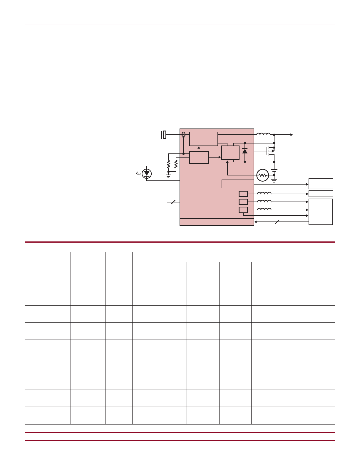
LTC3555/LTC3555-X
TRIPLE
HIGH EFFICIENCY
STEP-DOWN
SWITCHING
REGULATORS
I2C PORT
ALWAYS ON LDO
MEMORY
RTC/LOW
POWER LOGIC
I2C
CORE
I/O
µPROCESSOR
USB/WALL
4.35V TO 5.5V
CHARGE
ENABLE
CONTROLS
USB COMPLIANT
STEP-DOWN
REGULATOR
CC/CV
BATTERY
CHARGER
5
1
2
3
CURRENT
CONTROL
New Family of Integrated Power
Controllers Combine Fast Battery
Charging, PowerPath Control and
Efficient DC/DC Converters in
Less Than 20mm2
Introduction
The quickest way to build an efficient
power system for a battery-powered
portable application is to use an
IC that combines all power control
functions into a single chip, namely a
Power Management Integrated Circuit
(PMIC). PMICs seamlessly manage
power flow from various power sources
(wall adapters, USB and batteries) to
power loads (device systems and the
charging battery), while maintaining
current limits where required (such
as that specified for USB). To this
end, PMICs typically feature built-in
PowerPath™ control, DC/DC conver-
Table 1. Power management ICs with Li-ion/polymer battery chargers
PowerPath
Part Number
LTC3555/-1/-3 Switching I2C 1A, 400mA × 2 25mA
Topology Interface
Figure 1. High efficiency PowerPath manager and triple step-down regulator
Integrated Converters and Load Current Capabilities
by Sam Nork
PackageBuck Buck-Boost Boost LDO
4mm × 5mm
QFN-28
LTC3556 Switching I2C 400mA × 2 1A 25mA
LTC3566 Switching 1A 25mA
LTC3567 Switching I2C 1A 25mA
LTC3586* Switching 400mA × 2 1A 0.8A 20mA
LTC3557/-1 Linear 600mA, 400mA × 2 25mA
Linear Technology Magazine • September 2008
LTC3455 Linear 600mA, 400mA Controller
LTC3558 400mA 400mA
LTC3559/-1 400mA × 2
*For an application of the LTC3586 see “Complete Power Solution for Digital Cameras and Other Complex Compact Portable Applications” in this issue
4
4mm × 5mm
QFN-28
4mm × 4mm
QFN-24
4mm × 4mm
QFN-24
4mm × 6mm
QFN-38
4mm × 4mm
QFN-28
4mm × 4mm
QFN-24
3mm × 3mm
QFN-20
3mm × 3mm
QFN-16
DESIGN FEATURES L
Li-Ion
PGOODALL
0.8V TO 3.6V/400mA
3.3V/25mA
2.5V to 3.3V/1A
0.8V TO 3.6V/400mA
OPTIONAL
0V
T
TO OTHER
LOADS
+
LTC3556
DUAL HIGH EFFICIENCY
BUCKS
HIGH EFFICIENCY
BUCK-BOOST
I2C PORT
ALWAYS ON LDO
MEMORY
CORE
µP
RTC/LOW
POWER LOGIC
HDD/IO
3556 TA01
USB/WALL
4.5V TO 5.5V
CHARGE
I2C
USB COMPLIANT
STEP-DOWN
REGULATOR
CC/CV
BATTERY
CHARGER
SEQ
ENALL
3
1
2
3
40
50
60
70
80
30
20
10
0
90
100
V
IN3
(V)
2.7
EFFICIENCY (%)
3.1
3.5 3.9 4.3 4.7
V
OUT3
= 3.3V
TA = 27°C
I
OUT3
= 200mA
I
OUT3
= 50mA
I
OUT3
= 1000mA
BATTERY VOLTAGE (V)
2.8
0
CHARGE CURRENT (mA)
200
3.2
3.6
3.8
100
700
400
500
600
300
3
3.4
4
4.2
BATTERY CHARGE CURRENT
500mA USB CURRENT LIMIT
EXTRA CURRENT
FOR FASTER CHARGING
V
BUS
= 5V
5X MODE
BATTERY CHARGER PROGRAMMED FOR 1A
sion and battery charging functions.
PMICs can be applied in everything
from consumer electronics such as
MP3 players and Bluetooth headsets
to specialized portable medical and
industrial equipment.
Table 1 shows the wide variety of
integrated charger and DC/DC combinations now available from Linear
Technology. The latest additions to
the family, the LTC3555, LTC3556,
LTC3566, LTC3567 and LTC3586, are
primarily targeted toward relatively
high power Li-Ion applications and
contain blocks capable of high efficiency at high current levels. (To see
an application of the LTC3586, see
“Complete Power Solution for Digital
Cameras and Other Complex Compact
Portable Applications” in the Design
Ideas section of this issue.)
The most noteworthy feature of the
new parts is the use of a proprietary
switching PowerPath design, which
improves efficiency over linear power
path or battery fed solutions.
Switching PowerPath Control
Efficiently Harnesses
Available External Power
To speed up charging, some of Linear’s
new PMICs employ a unique current
limited synchronous buck switching charger architecture that uses
more power from the USB or adapter
than other topologies. This is a big
improvement over battery fed and
linear PowerPath control schemes.
(For a more detailed description of
the switching PowerPath architecture,
on” capability if the battery is dead or
missing (as long as the load current
is less than the input current limit).
However, neither a linear charger nor
linear power manager is well-suited
for high current charging due to poor
efficiency under certain conditions.
power, but charging/powering from
the USB host is complicated by the
host’s 2.5W limit. To take advantage of
the limited USB power, all components
Figure 2. Switching power manager charge
current vs battery voltage with a 500mA input
current limit. Peak charge current = 700mA.
in the power path must be as efficient
as possible.
is a battery-tracking (Bat-Track™)
see the cover article in the June 2008
issue of Linear Technology magazine
titled “Speed Up Li-ion Battery Charging and Reduce Heat with a Switching
PowerPath Manager.”)
For instance, portable products
with large capacity batteries (1Ahr
plus) face a direct tradeoff between
charge time and charger power dissipation—especially when a linear
charging method is used. At relatively
low charge currents, a linear charger
dissipates a modest amount of power,
but at currents required to quickly
charge high capacity batteries, a linear
charger can dissipate 2W or more.
A switching PowerPath topology is
an improvement over the commonly
synchronous buck design with logic
programmable input current limit to
ensure USB compatibility. When USB
or adapter power is available, the
LTC35xx power manager generates a
V
The 300mV difference voltage is sufficient to keep the battery charger
just out of dropout and deliver the
programmed charge current at high
efficiency. As with linear power managers, the load current is provided first,
and current that is left over is directed
to the battery. Input current limit is
controlled via an external resistor to
set absolute current and two logic
pins to control the ratio (e.g. 100mA,
500mA, 1A and Suspend).
used linear PowerPath topology, and
both are an improvement over battery
fed applications. A linear PowerPath
powers the application directly from
an external source rather than from
the battery itself and provides “instant
with a completely discharged battery
is achievable vs 60% or so for a linear
charger. Or said another way, the
switching power path dissipates only
50% of the power dissipated by a linear
USB is now a common source of
A key attribute in these new PMICs
supply equal to V
OUT
+ 300mV.
BAT
Charging efficiency of over 80%
Linear Technology Magazine • September 2008
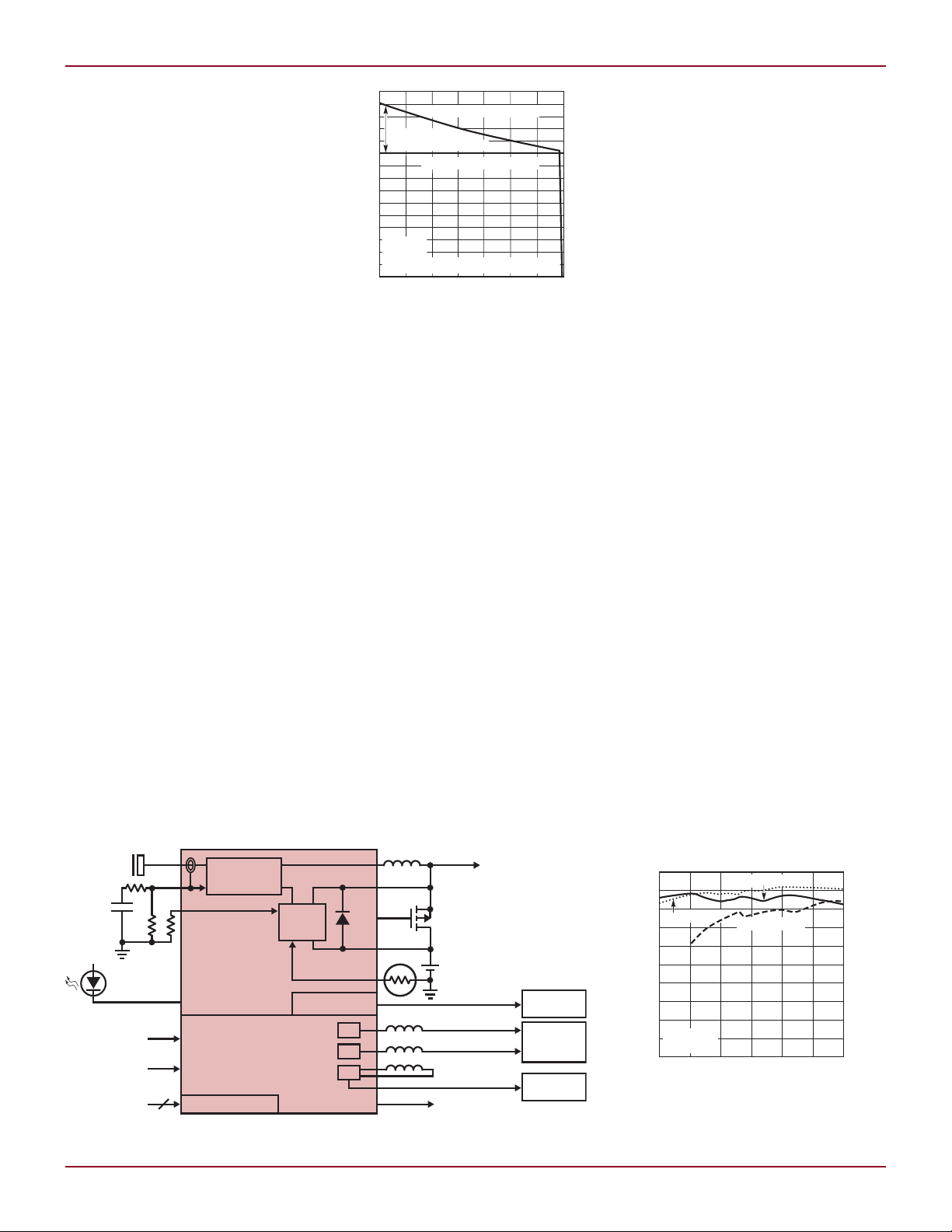
Figure 3. 1A buck-boost efficiency vs VIN (LTC3556, LTC3566/7, LTC3586)
5

GND
ILIM
DECODE
LOGIC
I2C PORT
SWAB1
V
IN1
V
C1
FB1
DV
CC
SCL
EN1
CHRGEN
CHRGEN
SDA
1A, 2.25MHz
BUCK-BOOST
REGULATOR
ENABLE
MODE
SWCD1
V
OUT1
D/A
4
6, 12, 17, 25
V
IN4
LTC3586
L
SW4
R1 C
OUT
C
PL
R2
V
OUT4
FB4
Li-Ion
FAULT
0.8V TO 3.6V/400mA
5V/800mA
3.3V/20mA
2.5V to 3.3V/1A
0.8V TO 3.6V/400mA
OPTIONAL
0V
T
TO OTHER
LOADS
+
LTC3586
DUAL HIGH EFFICIENCY
BUCKS
HIGH EFFICIENCY
BUCK-BOOST
HIGH EFFICIENCY
BOOST
ALWAYS ON LDO
MEMORY/
CORE µP
RTC/LOW
POWER LOGIC
I/O
SYSTEM
USB/WALL
4.5V TO 5.5V
CHARGE
I
LIM
USB COMPLIANT
STEP-DOWN
REGULATOR
CC/CV
BATTERY
CHARGER
MODE
EN
2
4
1
2
AUDIO/
MOTOR
4
3
CURRENT
CONTROL
L DESIGN FEATURES
charger under worst case conditions.
The LTC35xx switching power managers can charge at up to 1.2A max
and provide seamless switchover to
battery power when the external power
is removed. In USB applications, the
constant power (vs constant current)
nature of the switching PowerPath
controller makes it possible to charge
with more than 500mA from a fixed
500mA USB input source, as shown
in Figure 2.
Higher Current Chargers Go
Hand-In-Hand with Higher
Current Regulators
An obvious companion to a high
performance battery charger is a corresponding set of DC/DC regulators
with similar peak current handling
and high efficiency. As shown in Table
1, the latest PMICs offer between one
and four DC/DCs of varied topologies
with peak currents reaching 1A. The
new parts provide a variety of specific
options to meet the high performance
needs of specific applications.
Need a Buck-Boost?
Not a Problem…
Most high end portable products need
a minimum of three key power supplies: one for the µP core (~1.0V–1.5V),
one for memory (~1.8V), and one for
the I/O and main system supply
(~3.3V). The LTC3555 covers all three
with its built-in three synchronous
bucks. However, some applications,
particularly the more feature-rich variety, face occasional high peak power
transients during wireless transmissions or when a hard drive spins up.
The effective voltage of the battery
drops during these transient currents
due to the battery series resistance
Figure 5. Boost converter application circuit
6
Figure 4. The LTC3586 is a high efficiency PowerPath controller, alwayson LDO, dual buck, buck-boost, plus boost—all in a 4mm × 6mm package
(BSR), trace impedance or power path
losses. This poses a problem for the
3.3V supply, which can drop out of
regulation even if the battery is still
significantly charged. In such cases,
a buck-boost regulator can save the
day by riding through such battery
transients—maintaining regulation
as if nothing happened. Several new
PMICs contain buck-boost DC/DCs
specifically for this purpose. As shown
in Figure 3, the PMIC buck-boosts can
provide a high efficiency 3.3V output
with an input that ranges from 2.7V
to 5.5V.
The LTC3566 and LTC3567 products include a 1A buck-boost supply
in addition to a high performance
Figure 6. The LTC3567 I/O and DC/DC output voltage control interface
switching PowerPath controller as cornerstone high performance building
blocks. The LTC3556 ups the integration further by including two 400mA
buck regulators to accompany the
charger and buck-boost supply. The
LTC3586 contains all of the blocks of
the LTC3556, but ups the integration
one step further…
Need an Additional 5V Boost?
The LTC3586 Has It Covered
While the buck-boost regulators are
capable of regulating a 5V supply,
some applications require both. To
meet this need, the LTC3586 includes
not only a full complement of low voltage regulators, it also includes a high
continued on page 15
Linear Technology Magazine • September 2008

DESIGN FEATURES L
the range of 1.4V to 3.3V. If possible,
using a lower OV
can reduce power
DD
consumption. The termination scheme
is largely based on the receiver. When
choosing the OV
voltage, refer to the
DD
receiver’s data sheet to terminate the
CML lines properly.
CML uses true double termination.
Generally, LVDS is only terminated at
the receiver, which means that any
signal reflection back to the source
reflects back to the receiver with little
attenuation. This limits the data rate
and trace length that LVDS can drive.
The truly differential nature of CML
radiates less energy than LVDS and
CMOS signals, allowing devices to be
in closer proximity to antennas, mixers or other sensitive analog front end
systems. CML also has common mode
termination. This gives CML a better
common mode behavior than LVDS.
LVDS is only terminated differentially,
which does not reject any common
mode signal that may appear on the
transmission line—another limiting
factor in LVDS signaling.
CML Power Consumption
With a constant 16mA of bias current
and a voltage swing of 800mV differential, CML logic consumes a moderate
amount of power. For an equal data
rate, CML logic consumes less total
power than PECL and LVPECL. A
single CML driver uses more power
than a single LVDS driver, but only
marginally more that the three pairs
of LVDS drivers required for a typical
LVDS serial bus.
8B/10B Encoding Makes for
Simple Connection
The 8B/10B encoding process results
in an average DC offset of zero, allowing
the data to be routed through transformers or fiber channel transceivers
that can provide isolation between
the digital and analog realm. 8B/10B
encoding also does not require a framing signal or a data clock, whereas
both are required in traditional serial
communication. 8B/10B encoding
transmits data over a single pair of
data lines, whereas a typical serial
ADC requires three or more pairs,
and a typical parallel ADC can require
more than 16 pairs.
The complexity of decoding 8B/10B
lies in the receiver. Fortunately Xilinx,
Altera and Lattice have solutions to
receive data from the LTC2274 and
decode the 8B/10B data, simplifying
the collection of 8B/10B data. Other
8B/10B decoding solutions may be
available. The FPGA required to receive
data from the LTC2274 must be able
to receive high speed serial transmissions of 2GHz or more.
Conclusion
Without sacrificing resolution or
sample rate, the LTC2274 delivers full
16-bit performance at 105Msps over
a single pair of transmission lines,
greatly simplifying layout and saving
valuable board space. This mitigates
interaction with other circuitry in
software defined radio, base station or
industrial applications which involve
many channels of an ADC routed to
one FPGA.
L
LTC35xx, continued from page 6
power synchronous boost converter
(Figure 5).
The fully integrated boost in the
LTC3586 can regulate up to a 5V output with up to 800mA from a battery
voltage as low as 3V. The regulator has
built in output disconnect making it
well-suited for USB OTG supplies or
for powering motors in printer and
camera applications. The current
mode synchronous boost is internally
compensated and operates at a fixed
2.25MHz switching frequency. Pulseskipping at low loads achieves low
noise output for driving high power
audio circuits.
I2C, Programmable
Sequencing and Easy I/O
Despite the progress in new cutting
edge features and design, one old
problem does not go away: power
supply control. Power supplies require
startup and power down sequencing,
fault detection/reporting/handling
and voltage and operating mode adjustments. Getting it all right can be
a system control nightmare depending
on the complexity and limitations of
the power supply circuits.
The LTC35xx family provides very
simple and flexible control of all essential power supply functions. The
LTC3566 and LTC3586 employ dedicated I/O control pins for enabling,
disabling and changing DC/DC
operating modes. Voltages on these
parts are fixed and set with external resistor dividers. The LTC3555,
LTC3556 and LTC3567 accommodate
either I2C control or simple I/O pins
to control the supplies. The LTC3556
provides a three-state SEQ pin to allow the power up sequence of its three
DC/DC converters to be programmed
via pin-strapping. Those parts with
I2C V
maximum V
control power-up at their
OUT
(as determined by the
OUT
FB servo point and external dividers)
when enabled via simple I/O, and
can independently reduce V
OUT
by as
much as 50% in equal 16-step increments via I2C.
All DC/DC converters in all the
PMICs discussed here can survive
an indefinite output fault. The parts
all provide a RST output and all converters are actively pulled down in
shutdown to ensure proper power-up
sequencing. The LTC3586 contains an
additional fault handing feature that
automatically powers down all DC/DC
converters whenever a valid fault is
detected. In short, the entire family
is designed for simple, flexible and
trouble-free control and operation.
Conclusion
Linear Technology’s latest PMIC
products improve the performance
and simplify the design of a wide variety of portable power management
applications. Instead of kitchen sink
alternatives with large packages,
Linear Technology offers a number of
devices with various feature mixes in
small packages. These new PMICs are
simple to use, highly integrated and
high performance, allowing for shorter
design times, greater PCB flexibility,
and better power/thermal management than traditional solutions.
L
Linear Technology Magazine • September 2008
15
 Loading...