

FEATURES
LTC3542
500mA, 2.25MHz
Synchronous Step-Down
DC/DC Converter
U
DESCRIPTIO
■
High Effi ciency: Up to 96%
■
High Peak Switch Current: 1000mA
■
Low Output Ripple (<20mV
Typical)
P-P
Burst Mode Operation: Only 26µA
■
Very Low Quiescent Current: Only 26µA
■
2.5V to 5.5V Input Voltage Range
■
2.25MHz Constant Frequency Operation
■
1MHz to 3MHz External Frequency Synchronization
■
Low Dropout Operation: 100% Duty Cycle
■
No Schottky Diode Required
■
Internal Soft-Start Limits Inrush Current
■
0.6V Reference Allows Low Output Voltages
■
Shutdown Mode Draws <1µA Supply Current
■
±2% Output Voltage Accuracy
■
Current Mode Operation for Excellent Line and Load
Transient Response
■
Overtemperature Protected
■
Available in 6-Lead 2mm × 2mm DFN and Small TSOT
U
APPLICATIO S
■
Cellular Telephones
■
Wireless and DSL Modems
■
Digital Cameras
■
MP3 Players
■
PDAs and Other Handheld Devices
The LTC®3542 is a high effi ciency monolithic synchronous
buck converter using a constant frequency, current mode
architecture. Supply current during operation is only
26µA, dropping to <1µA in shutdown. The 2.5V to 5.5V
input voltage range makes the LTC3542 ideally suited for
single Li-Ion battery-powered applications. 100% duty
cycle provides low dropout operation, extending battery
life in portable systems. The output voltage is adjustable
from 0.6V to V
. Internal power switches are optimized
IN
to provide high effi ciency and eliminate the need for an
external Schottky diode.
Switching frequency is internally set at 2.25MHz, allowing
the use of small surface mount inductors and capacitors,
and it can synchronize to an external clock signal with a
frequency range of 1MHz to 3MHz through the MODE/
SYNC pin. The LTC3542 is specifi cally designed to work
well with ceramic output capacitors, achieving very low
output voltage ripple and a small PCB footprint.
The LTC3542 can be confi gured for the power saving Burst
®
Mode
Operation. For reduced noise and RF interference,
the MODE/SYNC pin can be confi gured for pulse skipping
operation.
, LTC, LT and Burst Mode are registered trademarks of Linear Technology Corporation.
All other trademarks are the property of their respective owners.
Protected by U.S. Patents, including 5481178, 6580258, 6304066, 6127815, 6498466,
6611131, 5994885.
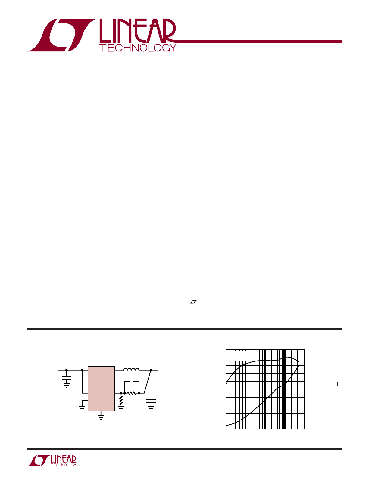
TYPICAL APPLICATIO
V
2.7V TO 5.5V
IN
C
10µF
CER
IN
V
IN
LTC3542
RUN
MODE/SYNC
GND
SW
V
FB
U
2.2µH
75k
22pF
150k
V
1.8V
500mA
C
OUT
10µF
CER
3542 TA01a
OUT
Effi ciency and Power Loss vs Output Current
100
VIN = 3.6V
90
= 1.8V
V
OUT
80
70
60
50
40
EFFICIENCY (%)
30
20
10
0
0.1 10 100 1000
1
OUTPUT CURRENT (mA)
1000
100
10
1
0.1
3542 TA01b
POWER LOSS (mW)
3542f
1
LTC3542
/
WWWU
ABSOLUTE AXI U RATI GS
(Note 1)
Input Supply Voltage (VIN) ........................... –0.3V to 6V
, RUN Voltages .......................................–0.3V to V
V
FB
MODE Voltage ................................–0.3V to (VIN + 0.3V)
SW Voltage ....................................–0.3V to (V
+ 0.3V)
IN
Operating Ambient Temperature Range
Junction Temperature (Note 7) ............................. 125°C
Storage Temperature Range ................... –65°C to 125°C
IN
Lead Temperature (Soldering, 10 sec)
TSOT-23 ............................................................ 300°C
Refl ow Peak Body Temperature (DFN) .................. 260°C
(Note 2) .................................................... –40°C to 85°C
UU
W
PACKAGE/ORDER I FOR ATIO
TOP VIEW
6
V
1
FB
2
3
DC PACKAGE
7
V
IN
GND
6-LEAD (2mm × 2mm) PLASTIC DFN
T
= 125°C, θJA = 40°C/W, θJC = 3°C/W (SOLDERED TO A 4-LAYER BOARD, NOTE 3)
JMAX
EXPOSED PAD (PIN 7) IS PGND, MUST BE SOLDERED TO PCB
RUN
MODE
5
SYNC
SW
4
GND 2
ORDER PART NUMBER DC PART MARKING ORDER PART NUMBER S6 PART MARKING
LTC3542EDC LCFR LTC3542ES6 LCFS
Order Options Tape and Reel: Add #TR
Lead Free: Add #PBF Lead Free Tape and Reel: Add #TRPBF
Lead Free Part Marking: http://www.linear.com/leadfree/
Consult LTC Marketing for parts specifi ed with wider operating temperature ranges.
TOP VIEW
VIN 1
V
3
FB
S6 PACKAGE
6-LEAD PLASTIC TSOT-23
T
= 125°C, θJA = 250°C/W
JMAX
6 SW
5 MODE/SYNC
4 RUN
●
The
ELECTRICAL CHARACTERISTICS
temperature range, otherwise specifi cations are at T
SYMBOL PARAMETER CONDITIONS MIN TYP MAX UNITS
V
IN
I
FB
V
FB
ΔV
LINE_REG
ΔV
LOAD_REG
I
S
f
OSC
f
SYNC
I
LIM
R
DS(ON)
Operating Voltage Range
Feedback Input Current ±30 nA
Feedback Voltage (Note 4)
Reference Voltage Line Regulation (Note 4) VIN = 2.5V to 5.5V 0.04 0.2 %/V
Output Voltage Load Regulation (Note 4) I
Input DC Supply Current (Note 5)
Active Mode
Sleep Mode
Shutdown
Oscillator Frequency VFB = 0.6V
Synchronous Frequency VFB = 0.6V 1 3 MHz
Peak Switch Current VIN = 3V, VFB = 0.5V, Duty Cycle < 35% 650 1000 mA
P-Channel On Resistance (Note 6)
N-Channel On Resistance (Note 6)
= 25°C. VIN = 3.6V unless otherwise noted.
A
denotes the specifi cations which apply over the full operating
●
2.5 5.5 V
●
0.588 0.6 0.612 V
= 100mA to 500mA 0.02 0.2 %
LOAD
V
= 0.5V
FB
V
= 0.7V, MODE = 0V
FB
RUN = 0V
ISW = 100mA
I
= –100mA
SW
26
0.1
●
1.8 2.25 2.7 MHz
0.5
0.35
500
35
1
0.65
0.55
µA
µA
µA
3542f
2
Ω
Ω
LTC3542
The
ELECTRICAL CHARACTERISTICS
temperature range, otherwise specifi cations are at T
= 25°C. VIN = 3.6V unless otherwise noted.
A
●
denotes the specifi cations which apply over the full operating
SYMBOL PARAMETER CONDITIONS MIN TYP MAX UNITS
I
SW(LKG)
V
UVLO
V
RUN
RUN Leakage Current
I
RUN
V
MODE/SYNC
I
MODE/SYNC
Switch Leakage Current VIN = 5V, V
Undervoltage Lockout Threshold VIN Rising
V
Falling 1.8
IN
RUN Threshold
MODE/SYNC Threshold
MODE/SYNC Leakage Current
Note 1: Stresses beyond those listed under Absolute Maximum Ratings
may cause permanent damage to the device. Exposure to any Absolute
Maximum Rating condition for extended periods may affect device
reliability and lifetime. No pin should exceed 6V.
Note 2: The LTC3542 is guaranteed to meet performance specifi cations
from 0°C to 85°C. Specifi cations over the –40°C to 85°C operating
temperature range are assured by design, characterization and correlation
with statistical process controls.
Note 3: Failure to solder the Exposed Pad of the package to the PC board
will result in a thermal resistance much higher than 40°C/W.
= 0V, VSW = 0V or 5V ±0.01 ±1 µA
RUN
2.0
2.3 V
1.9
●
0.3 1.5 V
●
●
0.3 1.2 V
●
±0.01 ±1 µA
±0.01 ±1 µA
Note 4: The converter is tested in a proprietary test mode that connects
the output of the error amplifi er to the SW pin, which is connected to an
external servo loop.
Note 5: Dynamic supply current is higher due to the internal gate charge
being delivered at the switching frequency.
Note 6: The DFN switch on resistance is guaranteed by correlation to wafer
level measurements.
Note 7: T
dissipation P
T
is calculated from the ambient temperature TA and power
J
according to the following formula:
D
= TA + (PD) • (θJA).
J
UW
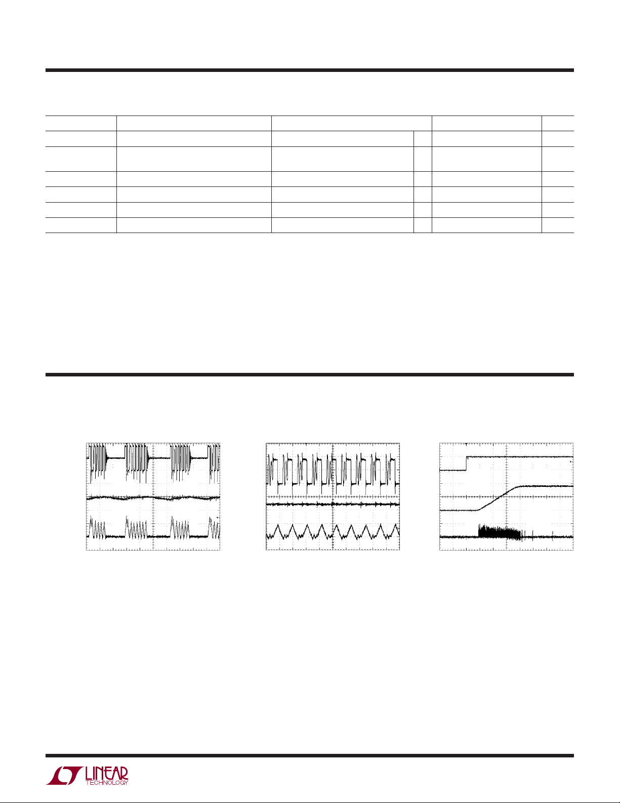
TYPICAL PERFOR A CE CHARACTERISTICS
TA = 25°C unless otherwise specifi ed.
V
SW
2V/DIV
V
OUT
50mV/DIV
AC COUPLED
100mA/DIV
Burst Mode Operation Pulse Skip Mode Operation Start-Up from Shutdown
RUN
2V/DIV
V
OUT
1V/DIV
100mA/DIV
I
L
V
= 3.6V
IN
= 1.8V
V
OUT
= 0A
I
LOAD
FIGURE 3a CIRCUIT
400µs/DIV
I
L
V
= 3.6V
IN
= 1.8V
V
OUT
= 25mA
I
LOAD
FIGURE 3a CIRCUIT
2µs/DIV
3542 G01
SW
2V/DIV
V
OUT
50mV/DIV
AC COUPLED
100mA/DIV
I
L
= 3.6V
V
IN
= 1.8V
V
OUT
= 25mA
I
LOAD
FIGURE 3a CIRCUIT
400ns/DIV
3542 G02
3542 G03
3542f
3
LTC3542
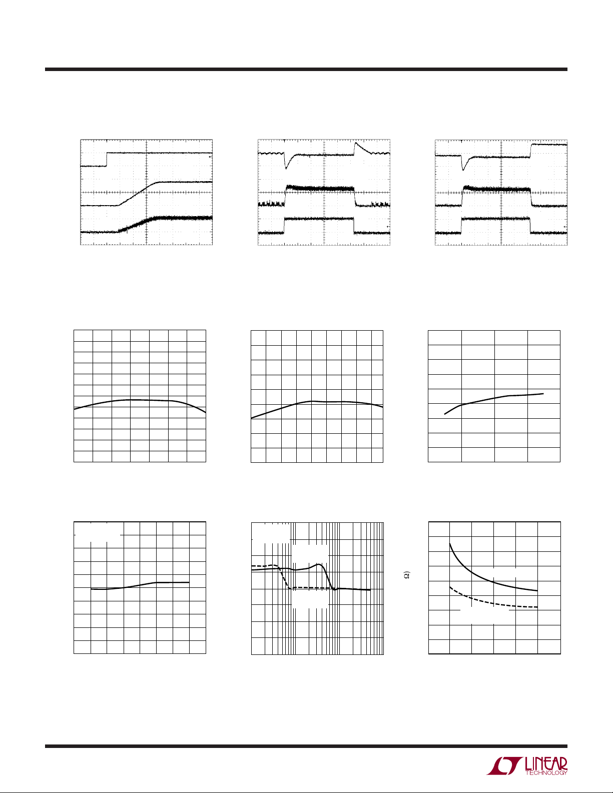
UW
TYPICAL PERFOR A CE CHARACTERISTICS
TA = 25°C unless otherwise specifi ed.
RUN
2V/DIV
V
OUT
1V/DIV
500mA/DIV
0.6150
0.6125
0.6100
0.6075
0.6050
0.6025
0.6000
(V)
0.5975
REF
V
0.5950
0.5925
0.5900
0.5875
0.5850
0.5825
Start-Up from Shutdown Load Step
V
OUT
100mV/DIV
AC COUPLED
I
L
500mA/DIV
I
L
V
= 3.6V
IN
= 1.8V
V
OUT
= 500mA
I
LOAD
FIGURE 3a CIRCUIT
Reference Voltage
vs Temperature
25
–50
0
–25
TEMPERATURE (°C)
400µs/DIV
50
3542 G04
100
125
3542 G07
75
I
LOAD
500mA/DIV
V
= 3.6V
IN
V
OUT
I
LOAD
FIGURE 3a CIRCUIT
Oscillator Frequency
vs Temperature
2.7
2.6
2.5
2.4
2.3
2.2
2.1
FREQUENCY (MHz)
2.0
1.9
1.8
–50 –30 –10 10 30 50 70 90 110
= 1.8V
= 30mA TO 500mA
20µs/DIV
TEMPERATURE (°C)
3542 G08
3542 G05
V
OUT
100mV/DIV
AC COUPLED
500mA/DIV
I
LOAD
500mA/DIV
2.7
2.6
2.5
2.4
2.3
2.2
2.1
FREQUENCY (MHz)
2.0
1.9
1.8
2
Load Step
I
L
= 3.6V
V
IN
= 1.8V
V
OUT
= 0mA TO 500mA
I
LOAD
FIGURE 3a CIRCUIT
20µs/DIV
Oscillator Frequency
vs Supply Voltage
3
4
SUPPLY VOLTAGE (V)
3542 G06
56
3542 G09
Output Voltage vs Supply Voltage
0.5
V
= 1.8V
OUT
0.4
= 100mA
I
OUT
0.3
0.2
0.1
0
ERROR (%)
–0.1
OUT
V
–0.2
–0.3
–0.4
–0.5
2
2.5 3.5
3
4
INPUT VOLTAGE (V)
4
4.5
vs Input Voltage
0.9
0.8
0.7
0.6
)
9
(
0.5
0.4
DS(ON)
R
0.3
0.2
0.1
0
R
1
DS(ON)
MAIN SWITCH
SYNCHRONOUS
SWITCH
32647
V
5
(V)
IN
3542 G12
3542f
Output Voltage vs Load Current
2.0
VIN = 3.6V
= 1.8V
V
OUT
1.5
1.0
0.5
0
ERROR (%)
–0.5
OUT
V
–1.0
–1.5
5.5
5
6
3542 G10
–2.0
1
Burst Mode
OPERATION
PULSE SKIP
MODE
10 100 1000
LOAD CURRENT (mA)
3542 G11
UW
TYPICAL PERFOR A CE CHARACTERISTICS
R
0.9
0.8
0.7
0.6
(Ω)
0.5
0.4
DS(ON)
R
0.3
0.2
0.1
0
–50
vs Temperature
DS(ON)
MAIN SWITCH
0
–25
TEMPERATURE (°C)
SYNCHRONOUS
SWITCH
VIN = 2.7V
= 3.6V
V
IN
= 4.2V
V
IN
25 125
50
75 100
3542 G13
Switch Leakage vs Input Voltage
1000
900
800
700
600
500
400
300
LEAKAGE CURRENT (pA)
200
100
0
0
SYNCHRONOUS
1
SWITCH
2
MAIN SWITCH
34
VIN (V)
TA = 25°C unless otherwise specifi ed.
Switch Leakage vs Temperature
300
250
200
150
100
SWITCH LEAKAGE (nA)
MAIN SWITCH
SYNCHRONOUS SWITCH
–25 0
25 75
TEMPERATURE (°C)
5
3542 G14
50
6
0
–50
LTC3542
50 100 125
3542 G15
Effi ciency vs Input Voltage
100
90
80
70
60
EFFICIENCY (%)
50
40
30
2.5
I
= 500mA
OUT
= 100mA
I
OUT
= 10mA
I
OUT
= 1mA
I
OUT
= 0.1mA
I
OUT
3 3.5
INPUT VOLTAGE (V)
V
= 1.8V
OUT
Burst Mode OPERATION
FIGURE 3a CIRCUIT
4.5 5.5
45
3542 G16
Effi ciency vs Load Current
100
90
80
70
60
50
40
EFFICIENCY (%)
30
20
V
= 1.8V
OUT
Burst Mode OPERATION
10
FIGURE 3a CIRCUIT
0
0.1 10 100 1000
1
OUTPUT CURRENT (mA)
Effi ciency vs Load Current Effi ciency vs Load Current
100
90
80
70
60
50
40
EFFICIENCY (%)
30
20
V
= 1.2V
OUT
Burst Mode OPERATION
10
FIGURE 3a CIRCUIT
0
0.1 10 100 1000
1
OUTPUT CURRENT (mA)
VIN = 2.7V
V
V
= 3.6V
IN
= 4.2V
IN
3542 G18
100
Burst Mode
90
OPERATION
80
70
60
50
40
EFFICIENCY (%)
30
20
10
0
0.1 10 100 1000
PULSE SKIP
1
OUTPUT CURRENT (mA)
VIN = 2.7V
V
V
MODE
VIN = 3.6V
= 1.8V
V
OUT
FIGURE 3a CIRCUIT
= 3.6V
IN
= 4.2V
IN
3542 G17
3542 G19
3542f
5

LTC3542
U
PI FU CTIO S
UU
(DFN/TSOT-23)
VFB (Pin 1/Pin 3): Output Feedback Pin. Receives the
feedback voltage from an external resistive divider across
the output. Nominal voltage for this pin is 0.6V.
(Pin 2/Pin 1): Power Supply Pin. Must be closely
V
IN
decoupled to GND.
GND (Pin 3/Pin 2): Ground Pin.
SW (Pin 4/Pin 6): Switch Node Connection to Inductor.
This pin connects to the drains of the internal main and
synchronous power MOSFET switches.
MODE/SYNC (Pin 5/Pin 5): Mode Selection and Oscillator
Synchronization Pin. This pin controls the operation of the
device. When tied to GND or V
, Burst Mode operation or
IN
W
BLOCK DIAGRA
pulse skipping mode is selected, respectively. Do not fl oat
this pin. The oscillation frequency can be synchronized to
an external oscillator applied to this pin and pulse skipping
mode is automatically selected.
RUN (Pin 6/Pin 4): Converter Enable Pin. Forcing this pin
above 1.5V enables this part, while forcing it below 0.3V
causes the device to shut down. In shutdown, all functions
are disabled drawing <1µA supply current. This pin must
be driven; do not fl oat.
GND (Pin 7, DFN Package Only): Exposed Pad. The Exposed Pad is ground. It must be soldered to PCB ground
to provide both electrical contact and optimum thermal
performance.
V
FB
0.6V
MODE/SYNC
RUN
–
EA
+
V
0.6V REF
IN
OSC
+
V
B
SHUTDOWN
–
+
MODE
DETECT
SLOPE COMPENSATION
BURST
MODE
CLKIN
LOGIC
I
COMP
ANTI-
SHOOT
THROUGH
I
RCMP
V
+
–
+
–
IN
SW
GND
3542 BD
6
3542f

OPERATIO
LTC3542
U
The LTC3542 uses a constant frequency, current mode,
step-down architecture. The operating frequency is set at
2.25MHz and can be synchronized to an external oscillator.
To suit a variety of applications, the selectable MODE/SYNC
pin allows the user to trade-off noise for effi ciency.
The output voltage is set by an external divider returned
to the V
output voltage with a reference voltage of 0.6V and adjusts
the peak inductor current accordingly.
Main Control Loop
During normal operation, the top power switch (P-channel
MOSFET) is turned on at the beginning of a clock cycle
when the V
current fl ows into the inductor and the load increases until
the current limit is reached. The switch turns off and energy
stored in the inductor fl ows through the bottom switch
(N-channel MOSFET) into the load until the next clock cycle.
The peak inductor current is controlled by the internally
compensated output of the error amplifi er. When the load
current increases, the V
the reference. This decrease causes the error amplifi er to
increase its output voltage until the average inductor current matches the new load current. The main control loop
is shut down by pulling the RUN pin to ground.
pin. An error amplifi er compares the divided
FB
voltage is below the reference voltage. The
FB
voltage decreases slightly below
FB
the sleep threshold and turns the top MOSFET on. This
process repeats at a rate that is dependent on the load
demand. By running cycles periodically, the switching
losses which are dominated by the gate charge losses of
the power MOSFETs are minimized.
For lower ripple noise at low load currents, the pulse skip
mode can be used. In this mode, the regulator continues
to switch at a constant frequency down to very low load
currents, where it will begin skipping pulses.
Dropout Operation
When the input supply voltage decreases toward the output
voltage, the duty cycle increases to 100%, which is the
dropout condition. In dropout, the PMOS switch is turned
on continuously with the output voltage being equal to the
input voltage minus the voltage drops across the internal
P-channel MOSFET and the inductor. An important design
consideration is that the R
increases with decreasing input supply voltage (See Typical
Performance Characteristics). Therefore, the user should
calculate the power dissipation when the LTC3542 is used
at 100% duty cycle with low input voltage (See Thermal
Considerations in the Applications Information Section).
Low Supply Operation
of the P-channel switch
DS(ON)
Low Load Current Operation
By selecting MODE/SYNC pin, two modes are available to
control the operation of the LTC3542 at low load currents.
Both modes automatically switch from continuous operation to the selected mode when the load current is low.
To optimize effi ciency, the Burst Mode operation can be
selected. When the converter is in Burst Mode operation,
the peak current of the inductor is set to approximately
60mA regardless of the output load. Each burst event can
last from a few cycles at light loads to almost continuously
cycling with short sleep intervals at moderate loads. In
between these burst events, the power MOSFETs and any
unneeded circuitry are turned off, reducing the quiescent
current to 26µA. In this sleep state, the load current is
being supplied solely from the output capacitor. As the
output voltage drops, the EA amplifi er’s output rises above
To prevent unstable operation, the LTC3542 incorporates
an undervoltage lockout circuit which shuts down the part
when the input voltage drops below about 2V.
Internal Soft-Start
At start-up when the RUN pin is brought high, the internal
reference is linearly ramped from 0V to 0.6V in about 1ms.
The regulated feedback voltage follows this ramp resulting
in the output voltage ramping from 0% to 100% in 1ms.
The current in the inductor during soft-start is defi ned
by the combination of the current needed to charge the
output capacitance and the current provided to the load
as the output voltage ramps up. The start-up waveform,
shown in the Typical Performance Characteristics, shows
the output voltage start-up from 0V to 1.8V with a 500mA
load and V
= 3.6V (refer to Figure 3a).
IN
3542f
7

LTC3542
WUUU
APPLICATIO S I FOR ATIO
A general LTC3542 application circuit is shown in Figure1.
External component selection is driven by the load requirement and begins with the selection of the inductor L. Once
the inductor is chosen, C
V
2.7V TO 5.5V
IN
C
Figure 1. LTC3542 General Schematic
IN
V
IN
LTC3542
RUN
MODE/SYNC
and C
IN
GND
SW
V
FB
can be selected.
OUT
L
C
F
R2
R1
C
3542 F01
V
OUT
OUT
Inductor Selection
The inductor value has a direct effect on ripple current ΔI
,
L
which decreases with higher inductance and increases with
higher V
∆I
L
=
IN
ƒ •
or V
V
OUT
O
, as shown in following equation:
OUT
⎛
–1
⎜
L
⎝
V
OUT
V
IN
⎞
⎟
⎠
where fO is the switching frequency. A reasonable starting
point for setting ripple current is ΔI
where I
OUT(MAX)
is 500mA. The largest ripple current ΔIL
= 0.4 • I
L
OUT(MAX)
,
occurs at the maximum input voltage. To guarantee that
the ripple current stays below a specifi ed maximum, the
inductor value should be chosen according to the following equation:
OUT
⎛
V
–
1
⎜
I
∆
V
⎝
IN MAX
V
L
=
ƒ •
OL
⎞
OUT
⎟
⎠
()
The DC current rating of the inductor should be at least
equal to the maximum load current plus half the ripple
current to prevent core saturation. Thus, a 600mA rated
inductor should be enough for most applications (500mA
+ 100mA). For better effi ciency, chose a low DC-resistance
inductor.
The inductor value will also have an effect on Burst Mode
operation. The transition to low current operation begins
when the inductor’s peak current falls below a level set by
the burst clamp. Lower inductor values result in higher
ripple current which causes the transition to occur at lower
load currents. This causes a dip in effi ciency in the upper
range of low current operation. In Burst Mode operation,
lower inductance values cause the burst frequency to
increase.
Inductor Core Selection
Different core materials and shapes change the size/current
and price/current relationships of an inductor. Toroid or
shielded pot cores in ferrite or permalloy materials are small
and don’t radiate much energy, but generally cost more
than powdered iron core inductors with similar electrical
characteristics. The choice of which style inductor to use
often depends more on the price vs size requirements
and any radiated fi eld/EMI requirements than on what the
LTC3542 requires to operate. Table 1 shows some typical surface mount inductors that work well in LTC3542
applications.
Input Capacitor (C
) Selection
IN
In continuous mode, the input current of the converter is a
square wave with a duty cycle of approximately V
OUT/VIN
.
To prevent large voltage transients, a low equivalent series
resistance (ESR) input capacitor sized for the maximum
RMS current must be used. The maximum RMS capacitor
current is given by:
VVV
II
≈
RMS MAX
OUT IN OUT
where the maximum average output current I
–
()
V
IN
equals
MAX
the peak current minus half the peak-to-peak ripple cur-
= I
rent, I
= 2V
V
IN
MAX
OUT
– ΔIL/2. This formula has a maximum at
LIM
, where I
RMS
= I
/2. This simple worst-case
OUT
is commonly used to design because even signifi cant
deviations do not offer much relief. Note that capacitor
manufacturer’s ripple current ratings are often based on
only 2000 hours life time. This makes it advisable to further
derate the capacitor, or choose a capacitor rated at a higher
temperature than required. Several capacitors may also be
paralleled to meet the size or height requirements of the
8
3542f

WUUU
APPLICATIO S I FOR ATIO
Table 1. Representative Surface Mount Inductors
PART NUMBER VALUE
MANUFACTURER
Sumida CDRH2D11-2RM 2.2 0.780 0.098 3.2 × 3.2 × 1.2
CDRH3D16 2.2 1.2 0.075 3.8 × 3.8 × 1.8
CMD4D11 2.2 0.95 0.116 4.4 × 5.8 × 1.2
CDH2D09B 3.3 0.85 0.15 2.8 × 3 × 1
Murata LQH32CN 2.2 0.79 0.097 2.5 × 3.2 × 1.55
LQH43CN 4.7 0.75 0.15 4.5 × 3.2 × 2.6
TDK IVLC453232 2.2 0.85 0.18 4.8 × 3.4 × 3.4
VLF3010AT-
2R2M1R0
MAX DC
CURRENT
(µH)
CLS4D09 4.7 0.75 0.15 4.9 × 4.9 × 1
2.2 1.0 0.12 2.8 × 2.6 × 1
(A)
DCR
(Ω) SIZE (mm3)
LTC3542
design. An additional 0.1µF to 1µF ceramic capacitor is
also recommended on V
for high frequency decoupling,
IN
when not using an all ceramic capacitor solution.
Output Capacitor (C
The selection of C
) Selection
OUT
is driven by the required ESR to
OUT
minimize voltage ripple and load step transients. Typically,
once the ESR requirement is satisfi ed, the RMS current
rating generally far exceeds the I
RIPPLE(P-P)
except for an all ceramic solution. The output ripple (ΔV
requirement,
)
OUT
is determined by:
∆∆V I ESR
≈+
OUT L
⎛
⎜
⎝
8• •ƒ
1
O
where fO is the switching frequency, C
capacitance and ΔI
is the inductor ripple current. For a fi xed
L
C
OUT
⎞
⎟
⎠
is the output
OUT
output voltage, the output ripple is highest at maximum
input voltage since ΔI
increases with input voltage.
L
If tantalum capacitors are used, it is critical that the capacitors are surge tested for use in switching power supplies.
An excellent choice is the AVX TPS series of surface mount
tantalums, available in case heights ranging from 2mm to
4mm. These are specially constructed and tested for low
ESR so they give the lowest ESR for a given volume. Other
capacitor types include Sanyo POSCAP, Kemet T510 and
T495 series, and Sprague 593D and 595D series. Consult
the manufacturer for other specifi c recommendations.
Ceramic Input and Output Capacitors
Higher value, lower cost ceramic capacitors are now
becoming available in smaller case sizes. Their high
ripple current rating, high voltage rating and low ESR
are tempting for switching regulator use. However, the
ESR is so low that it can cause loop stability problems.
Since the LTC3542’s control loop does not depend on
the output capacitor’s ESR for stable operation, ceramic
capacitors can be used to achieve very low output ripple
and small circuit size. X5R or X7R ceramic capacitors are
recommended because these dielectrics have the best
temperature and voltage characteristics of all the ceramics
for a given value and size.
Great care must be taken when using only ceramic input
and output capacitors. When a ceramic capacitor is used
at the input and the power is being supplied through long
wires, such as from a wall adapter, a load step at the output
can induce ringing at the V
pin. At best, this ringing can
IN
couple to the output and be mistaken as loop instability.
At worst, the ringing at the input can be large enough to
damage the part. For more information, see Application
Note 88. The recommended capacitance value to use is
10µF for both input and output capacitors.
3542f
9

LTC3542
WUUU
APPLICATIO S I FOR ATIO
Output Voltage Programming
The output voltage is set by a resistive divider according
to the following formula:
R
2
VV
=+
OUT
⎛
06 1
.
⎜
⎝
⎞
⎟
⎠
R
1
To improve the frequency response, a feed-forward capaci-
, may also be used. Great care should be taken to
tor, C
F
route the V
line away from noise sources, such as the
FB
inductor or the SW line.
Mode Selection and Frequency Synchronization
The MODE/SYNC pin is a multipurpose pin that provides
mode selection and frequency synchronization. Connecting this pin to GND enables Burst Mode operation, which
provides the best low current effi ciency at the cost of a
higher output voltage ripple. Connecting this pin to V
IN
selects pulse skip mode operation, which provides the
lowest output ripple at the cost of low current effi ciency.
The LTC3542 can also be synchronized to an external clock
signal with range from 1MHz to 3MHz by the MODE/SYNC
pin. During synchronization, the mode is set to pulse skip
and the top switch turn-on is synchronized to the falling
edge of the external clock.
Effi ciency Considerations
The effi ciency of a switching regulator is equal to the output
power divided by the input power times 100%. It is often
useful to analyze individual losses to determine what is
limiting the effi ciency and which change would produce
the most improvement. Effi ciency can be expressed as:
Although all dissipative elements in the circuit produce
losses, three main sources usually account for most of
the losses in LTC3542 circuits: 1) V
2
R loss and 3) switching loss. VIN quiescent current
2) I
quiescent current,
IN
loss dominates the power loss at very low load currents,
whereas the other two dominate at medium to high load
currents. In a typical effi ciency plot, the effi ciency curve
at very low load currents can be misleading since the
actual power loss is of no consequence as illustrated in
Figure 2.
1) The V
quiescent current is the DC supply current given
IN
in the Electrical Characteristics which excludes MOSFET
charging current. V
loss that increases with V
2
R losses are calculated from the DC resistances of
2) I
the internal switches, R
current results in a small (<0.1%)
IN
, even at no load.
IN
, and external inductor, RL. In
SW
continuous mode, the average output current fl ows through
inductor L, but is “chopped” between the internal top and
bottom switches. Thus, the series resistance looking into
the SW pin is a function of both top and bottom MOSFET
R
R
The R
and the duty cycle (D) as follows:
DS(ON)
= (R
SW
DS(ON)
DS(ON)TOP
for both the top and bottom MOSFETs can
)(D) + (R
DS(ON)BOT
)(1 – D)
be obtained from the Typical Performance Characteristics
2
curves. Thus, to obtain I
2
R losses = I
I
1000
OUT
VIN = 3.6V
Burst Mode OPERATION
100
R losses:
2
(RSW + RL)
Effi ciency = 100% – (L1 + L2 + L3 + ...)
where L1, L2, etc. are the individual losses as a percentage of input power.
10
10
POWER LOSS (mW)
1
0.1
0.1 10 100 1000
Figure 2. Power Loss vs Load Current
1
OUTPUT CURRENT (mA)
V
= 2.5V
OUT
= 1.8V
V
OUT
= 1.2V
V
OUT
3542 F02
3542f

WUUU
APPLICATIO S I FOR ATIO
LTC3542
3) The switching current is MOSFET gate charging current,
that results from switching the gate capacitance of the
power MOSFETs. Each time a MOSFET gate is switched
from low to high to low again, a packet of charge dQ moves
from V
V
IN
In continuous mode, I
and Q
to ground. The resulting dQ/dt is a current out of
IN
that is typically much larger than the DC bias current.
GATECHG
are the gate charges of the internal top and bottom
B
= fO(QT + QB), where QT
MOSFET switches. The gate charge losses are proportional
and thus their effects will be more pronounced at
to V
IN
higher supply voltages.
Other “hidden” losses such as copper trace and internal
battery resistances can account for additional effi ciency
degradations in portable systems. The internal battery
and fuse resistance losses can be minimized by making
sure that C
has adequate charge storage and very low
IN
ESR at the switching frequency. Other losses include
diode conduction losses during dead-time and inductor
core losses generally account for less than 2% total additional loss.
The junction temperature, TJ, is given by:
= TA + T
T
J
R
where TA is the ambient temperature.
As an example, consider the LTC3542 in dropout at an
input voltage of 2.7V, a load current of 500mA and an
ambient temperature of 70°C. From the typical performance
graph of switch resistance, the R
of the P-channel
DS(ON)
switch at 70°C is approximately 0.7Ω. Therefore, power
dissipated by the part is:
LOAD
2
• R
DS(ON)
= 175mW
is 40°C/W. Thus, the junction
JA
= I
P
D
For the DFN package, the θ
temperature of the regulator is:
= 70°C + 0.175 • 40 = 77°C
T
J
which is below the maximum junction temperature of
125°C.
Note that at higher supply voltages, the junction temperature
is lower due to reduced switch resistance (R
DS(ON)
).
Thermal Considerations
In most applications the LTC3542 does not dissipate much
heat due to its high effi ciency. But in applications where the
LTC3542 is running at high ambient temperature with low
supply voltage and high duty cycles, such as in dropout,
the heat dissipated may exceed the maximum junction
temperature of the part. If the junction temperature reaches
approximately 150°C, both power switches will be turned
off and the SW node will become high impedance.
To avoid the LTC3542 from exceeding the maximum
junction temperature, the user need to do some thermal
analysis. The goal of the thermal analysis is to determine
whether the power dissipated exceeds the maximum
junction temperature of the part. The temperature rise is
given by:
= (PD)(θJA)
T
R
where P
θ
JA
is the power dissipated by the regulator and
D
is the thermal resistance from the junction of the die
to the ambient.
Checking Transient Response
The regulator loop response can be checked by looking
at the load transient response. Switching regulators take
several cycles to respond to a step in load current. When
a load step occurs, V
equal to ΔI
resistance of C
charge C
OUT
• ESR, where ESR is the effective series
LOAD
OUT
, generating a feedback error signal used by the
regulator to return V
this recovery time, V
immediately shifts by an amount
OUT
. ΔI
also begins to charge or dis-
LOAD
to its steady-state value. During
OUT
can be monitored for overshoot
OUT
or ringing that would indicate a stability problem.
The output voltage settling behavior is related to the stability
of the closed-loop system and will demonstrate the actual
overall supply performance. For a detailed explanation of
optimizing the compensation components, including a review of control loop theory, refer to Application Note 76.
In some applications, a more severe transient can be caused
by switching loads with large (>1µF) bypass capacitors.
The discharged bypass capacitors are effectively put in
3542f
11

LTC3542
WUUU
APPLICATIO S I FOR ATIO
parallel with C
, causing a rapid drop in V
OUT
. No regula-
OUT
tor can deliver enough current to prevent this problem, if
the switch connecting the load has low resistance and is
driven quickly. The solution is to limit the turn-on speed of
TM
the load switch driver. A Hot Swap
controller is designed
specifi cally for this purpose and usually incorporates current limit, short circuit protection and soft-start.
Design Example
As a design example, assume the LTC3542 is used in a single
lithium-ion battery-powered cellular phone application. The
will be operating from a maximum of 4.2V down to
V
IN
about 2.7V. The load current requirement is a maximum
of 0.5A, but most of the time it will be in standby mode,
requiring only 2mA. Effi ciency at both low and high load
currents is important. Output voltage is 1.8V.
With this information we can calculate L using:
1
L
=
•
∆
fI
L
Substituting V
⎛
••–
V
OUT
OUT
1
⎜
⎝
= 1.8V, VIN = 4.2V, ΔIL = 200mA and
V
OUT
V
IN
⎞
⎟
⎠
f = 2.25MHz gives:
V
18
L
2 25 200
.•
.
MHz mA
⎛
1
•–
⎜
⎝
18
.
42
.
V
⎞
⎟
⎠
V
=
228
.
µH=
CIN will require an RMS current rating of at least
0.25A ≅ I
LOAD(MAX)
/2 at temperature and C
will require
OUT
ESR of less than 0.2Ω. In most cases, ceramic capacitors
will satisfy these requirements. Select C
= 10µF.
C
IN
= 10µF and
OUT
For the feedback resistors, choose R1 = 75k, R2 can be
calculated from:
V
⎛
R
OUT
2
⎜
⎝
.
06
⎞
–•
11
⎟
⎠
V
R
.
V
18
⎛
=
⎜
⎝
.
06
⎞
–• ==150k
V
k
175=
⎟
⎠
Figure 3 shows the complete circuit along with its effi ciency
curve, load step response and recommended layout
PC Board Layout Checklist
When laying out the printed circuit board, the following
checklist should be used to ensure proper operation of
the LTC3542. These items are also illustrated graphically
in Figure 3b. Check the following in your layout:
1. The power traces, consisting of the GND trace, the SW
trace and the V
trace should be kept short, direct and
IN
wide.
2. Does the V
pin connect directly to the feedback re-
FB
sistors? The resistive divider R1/R2 must be connected
between the (+) plate of C
and ground.
OUT
Choosing a vendor’s closest inductor value of 2.2µH results
in a maximum ripple current of:
V
18
∆I
=
L
225 22
.
MHz µH
.•.
⎛
1
•–
⎜
⎝
18
.
42
.
V
⎞
=
207
⎟
⎠
V
.88mA
12
3. Does the (+) plate of C
connect to VIN as closely as
IN
possible? This capacitor provides the AC current to the
internal power MOSFETs.
4. Keep the (–) plates of C
and C
IN
as close as pos-
OUT
sible.
5. Keep the switching node, SW, away from the sensitive
node.
V
FB
Hot Swap is a trademark of Linear Technology Corporation.
3542f

WUUU
APPLICATIO S I FOR ATIO
V
2.7V TO 5.5V
IN
L*
2.2µH
22pF
C
F
R2
150k
FB
R1
75k
C
IN
10µF
**
V
SW
IN
LTC3542
RUN
V
MODE/SYNC
GND
*SUMIDA CDRH2D18HD-2R2NC
**TDK C2012X5R0J106M
Figure 3a. Typical Application
R1
C
F
R2
GND
C
10µF
3542 F03a
V
OUT
1.8V
500mA
**
OUT
LTC3542
100
90
80
70
60
50
40
EFFICIENCY (%)
30
20
V
= 1.8V
OUT
Burst Mode OPERATION
10
FIGURE 3a CIRCUIT
0
0.1 10 100 1000
1
OUTPUT CURRENT (mA)
VIN = 2.7V
V
V
V
= 3.6V
IN
= 4.2V
IN
IN
V
FB
V
IN
C
IN
GND
GND
Figure 3b. Layout Diagram
3542 G17
VIA TO V
1
2
GND
3
C
OUT
RUN
6
MODE/
5
SYNC
4
SW
V
OUT
V
OUT
100mV/DIV
AC COUPLED
500mA/DIV
I
LOAD
500mA/DIV
I
OUT
L
L
= 3.6V
V
IN
= 1.8V
V
OUT
= 0mA TO 500mA
I
LOAD
FIGURE 3a CIRCUIT
3542 F03b
20µs/DIV
3542 G06
Figure 3d. Load Step
Figure 3c. Effi ciency Curve
3542f
13

LTC3542
PACKAGE DESCRIPTIO
U
DC Package
6-Lead Plastic DFN (2mm × 2mm)
(Reference LTC DWG # 05-08-1703)
0.675 ±0.05
2.50 ±0.05
1.15 ±0.05
0.61 ±0.05
(2 SIDES)
0.50 BSC
1.42 ±0.05
(2 SIDES)
RECOMMENDED SOLDER PAD PITCH AND DIMENSIONS
PIN 1 BAR
TOP MARK
(SEE NOTE 6)
0.200 REF
NOTE:
1. DRAWING TO BE MADE A JEDEC PACKAGE OUTLINE M0-229 VARIATION OF (WCCD-2)
2. DRAWING NOT TO SCALE
3. ALL DIMENSIONS ARE IN MILLIMETERS
4. DIMENSIONS OF EXPOSED PAD ON BOTTOM OF PACKAGE DO NOT INCLUDE
MOLD FLASH. MOLD FLASH, IF PRESENT, SHALL NOT EXCEED 0.15mm ON ANY SIDE
5. EXPOSED PAD SHALL BE SOLDER PLATED
6. SHADED AREA IS ONLY A REFERENCE FOR PIN 1 LOCATION ON THE
TOP AND BOTTOM OF PACKAGE
PACKAGE
OUTLINE
0.25 ± 0.05
2.00 ±0.10
(4 SIDES)
0.75 ±0.05
0.00 – 0.05
R = 0.115
TYP
0.56 ± 0.05
(2 SIDES)
1.37 ±0.05
BOTTOM VIEW—EXPOSED PAD
3
(2 SIDES)
0.38 ± 0.05
64
1
0.50 BSC
PIN 1
CHAMFER OF
EXPOSED PAD
(DC6) DFN 1103
0.25 ± 0.05
14
3542f

PACKAGE DESCRIPTIO
LTC3542
U
S6 Package
6-Lead Plastic TSOT-23
(Reference LTC DWG # 05-08-1636)
0.62
MAX
3.85 MAX
2.62 REF
RECOMMENDED SOLDER PAD LAYOUT
PER IPC CALCULATOR
0.20 BSC
DATUM ‘A’
NOTE:
1. DIMENSIONS ARE IN MILLIMETERS
2. DRAWING NOT TO SCALE
3. DIMENSIONS ARE INCLUSIVE OF PLATING
4. DIMENSIONS ARE EXCLUSIVE OF MOLD FLASH AND METAL BURR
5. MOLD FLASH SHALL NOT EXCEED 0.254mm
6. JEDEC PACKAGE REFERENCE IS MO-193
0.95
REF
1.22 REF
1.4 MIN
0.30 – 0.50 REF
2.80 BSC
0.09 – 0.20
(NOTE 3)
1.50 – 1.75
(NOTE 4)
1.00 MAX
0.95 BSC
0.80 – 0.90
2.90 BSC
(NOTE 4)
PIN ONE ID
0.30 – 0.45
6 PLCS (NOTE 3)
0.01 – 0.10
1.90 BSC
S6 TSOT-23 0302
Information furnished by Linear Technology Corporation is believed to be accurate and reliable.
However, no responsibility is assumed for its use. Linear Technology Corporation makes no representation that the interconnection of its circuits as described herein will not infringe on existing patent rights.
3542f
15

LTC3542
TYPICAL APPLICATIO
U
Using Low Profi le Components, <1mm Height
V
2.7V TO 5.5V
EFFICIENCY (%)
IN
CIN**
10mF
CER
2
V
IN
6
RUN
5
MODE/SYNC
LTC3542
GND
4
SW
1
V
FB
3
*TDK VLF3010AT-2R2MIR0
**TDK C2012X5R0J106M
Effi ciency vs Output Current
100
90
80
70
60
50
40
30
20
10
0
0.1 10 100 1000
VIN = 3.6V
= 1.5V
V
OUT
Burst Mode OPERATION
1
OUTPUT CURRENT (mA)
2.2mH*
22pF
150k
75k
3542 TA02b
V
1.5V
500mA
C
OUT
10mF
CER
3542 TA02a
OUT
**
RELATED PARTS
PART NUMBER DESCRIPTION COMMENTS
LTC3405/LTC3405B 300mA I
, 1.5MHz, Synchronous Step-Down DC/DC
OUT
Converter
LTC3406/LTC3406B 600mA I
, 1.5MHz, Synchronous Step-Down DC/DC
OUT
Converter
LTC3407/LTC3407-2 Dual 600mA/800mA I
Step-Down DC/DC Converter
LTC3409 600mA I
, 1.7MHz/2.6MHZ, Synchronous Step-Down
OUT
DC/DC Converter
LTC3410/LTC3410B 300mA I
, 2.25MHz, Synchronous Step-Down DC/DC
OUT
Converter
LTC3411 1.25A I
, 4MHz, Synchronous Step-Down DC/DC
OUT
Converter
LTC3548 Dual 400mA/800mA I
Step-Down DC/DC Converter
LTC3561 1A I
, 4MHz Synchronous Step-Down DC/DC Converter 95% Effi ciency, VIN: 2.6V to 5.5V, V
OUT
Linear Technology Corporation
16
1630 McCarthy Blvd., Milpitas, CA 95035-7417
(408) 432-1900 ● FAX: (408) 434-0507
, 1.5MHz/2.25MHz, Synchronous
OUT
, 2.25MHz, Synchronous
OUT
●
www.linear.com
95% Effi ciency, VIN: 2.5V to 5.5V, V
I
< 1µA, ThinSOT Package
SD
96% Effi ciency, VIN: 2.5V to 5.5V, V
I
< 1µA, ThinSOT Package
SD
95% Effi ciency, VIN: 2.5V to 5.5V, V
I
< 1µA, MS10E, DFN Packages
SD
96% Effi ciency, VIN: 1.6V to 5.5V, V
I
< 1µA, DFN Package
SD
95% Effi ciency, VIN: 2.5V to 5.5V, V
I
< 1µA, SC70 Package
SD
95% Effi ciency, VIN: 2.5V to 5.5V, V
I
< 1µA, MS10, DFN Packages
SD
95% Effi ciency, VIN: 2.5V to 5.5V, V
I
< 1µA, MS10, DFN Packages
SD
< 1µA, 3mm × 3mm DFN Package
I
SD
= 0.8V, IQ = 20µA,
OUT(MIN)
= 0.6V, IQ = 20µA,
OUT(MIN)
= 0.6V, IQ = 40µA,
OUT(MIN)
= 0.6V, IQ = 65µA,
OUT(MIN)
= 0.8V, IQ = 26µA,
OUT(MIN)
= 0.8V, IQ = 60µA,
OUT(MIN)
= 0.6V, IQ = 40µA,
OUT(MIN)
= 0.8V, IQ = 240µA,
OUT(MIN)
3542f
LT 0906 • PRINTED IN USA
© LINEAR TECHNOLOGY CORPORATION 2006
 Loading...