

Wide Input Voltage Range Buck-Boost Converter Simplifi es
Design of Variable Input Supplies –
Design Note DN413
John Canfi eld
Introduction
Many of today’s portable electronic devices require
the ability to operate from a variety of power sources
including USB, wall adapters, and alkaline and lithium
batteries. Designing a power conversion solution that
is compatible with this wide array of power sources can
®
be daunting. The LTC
3530 monolithic synchronous
converter simplifi es the task by operating in both buck
and boost modes over an extended input voltage range
of 1.8V to 5.5V. No complicated topology is required to
account for varying inputs that can be above, below or
equal to the output.
The LTC3530 utilizes a proprietary switching algorithm
that provides seamless transitions between buck and
boost modes while simultaneously optimizing effi ciency
over all operating condi tions. Using this advanced control
algorithm, the LTC3530 is c apable of high effi ciency, fi xed
frequency operation with input voltages that are above,
below, or equal to the output voltage, while requiring only
a single inductor. This capability makes the LTC3530 well
suited for lithium- ion/polymer and 2-cell alkaline or NiMH
applications which require a supply voltage that is within
the bat tery voltage r ange. In such cases, the high ef fi ciency
and extended input operating range of the LTC3530 offer
greatly improved battery run-time, as much as 25% in
some cases, over alternative solutions.
At 3.3V output, a load current of up to 600mA can be
supported over the entire lithium-ion input voltage range;
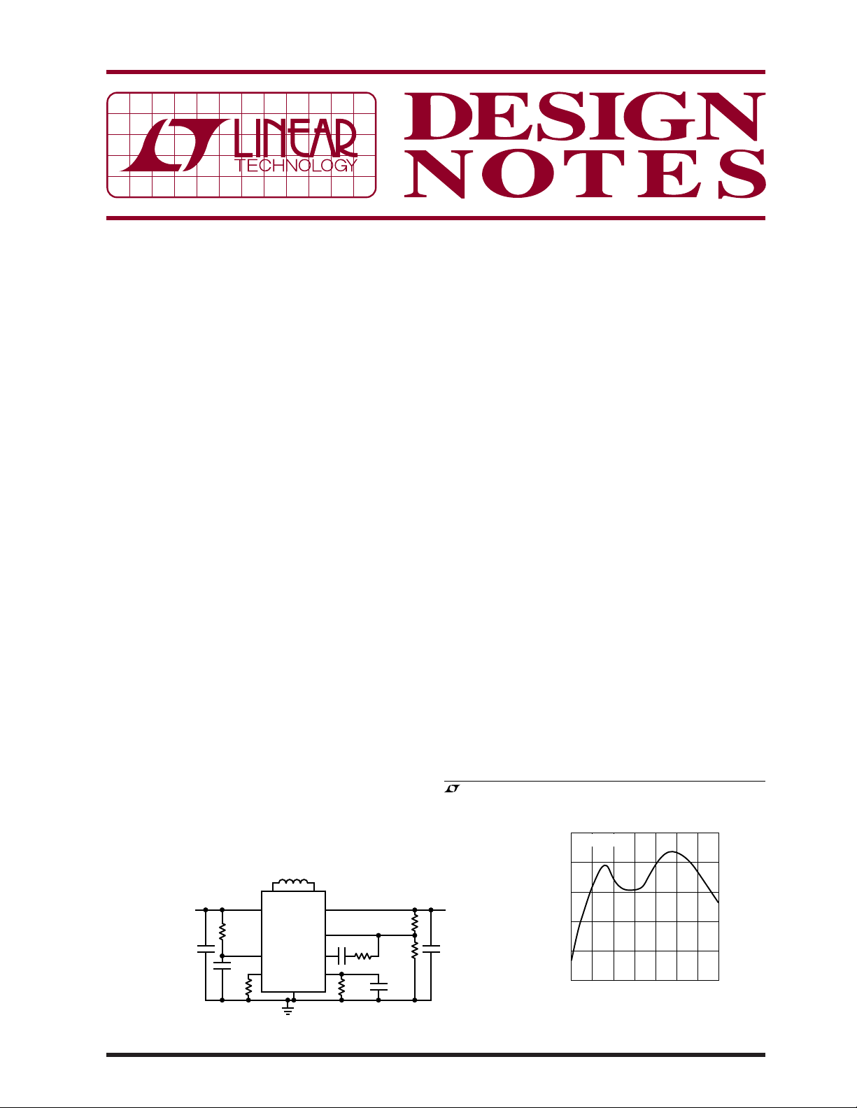
L1
4.7µH
V
IN
1.8V TO 5.5V
C
IN
10µF
Figure 1. 3.3V at 250mA from a 1.8V to 5.5V Input
SW1 SW2
V
V
IN
OUT
1M
0.01µF
33.2k 0.01µF
LTC3530
SHDN/SS
R
T
FB
330pF
V
C
BURST
GND
L1: TDK RLF7030T-4R7M3R4
100k
30.1k
340k
200k
250mA of load current is supported when the input is
1.8V. The ou tput voltage is user-programmable from 1.8V
to 5.25V via an external resistor divider. The LTC3530
includes a soft-star t circuit to minimize the inrush current
transient during power-up. The duration of the soft-start
period can be programmed via the time constant of an
external resistor and capacitor.
The switching frequency of the LTC3530 is user progr ammable via a single ex ternal resistor, allowing the converter
to be optimized to meet the space and effi ciency requirements of each particular application. An external resistor
and capacitor prov ide compensation of the feedback loop,
enabling the frequency response to be adjusted to suit a
wide array of external components. This fl exibility allows
for rapid output voltage transient response regardless of
inductor value and output capacitor size.
The LTC3530 features an automatic transition to Burst
Mode
to improve light load effi ciency. For noise sensitive applications, the LTC3530 c an be forced into fi xed fr equency
operation at all lo ad currents by co nnecting the BURST pin
to V
and overtemperature shutdown. Internal reverse current
limiting circuitry prevents damage to the part should
, LT, LTC, LTM and Burst Mode are registered trademarks of Linear Technology
Corporation. All other trademarks are the property of their respective owners.
V
OUT
3.3V
250mA
C
OUT
22µF
DN413 F01
®
operation at a user programmable current level
. The LTC3530 also fe atures short-circui t protection
IN
94
I
= 150mA
OUT
92
90
88
EFFICIENCY (%)
86
84
2
4
3
INPUT VOLTAGE (V)
5
DN413 F02
Figure 2. Effi ciency vs Input Voltage
of the Circuit in Figure 1
04/07/413
the output voltage be pulled above regulation through
an external path.
output voltage, and inductor value, unlike other devices
that rely on the level of peak inductor current.
Effi ciency
Figure 1 illustrates a typical LTC3530 application circuit
confi gured with a 1MHz switching frequency, which
represents a good compromise between the PCB area
and effi ciency for most applications. The effi ciency curve
versus input voltage for this application circuit is shown
in Figure 2. The LTC3530 achieves greater then 85%
effi ciency with an input voltage greater than or equal to
2V. These high levels of effi ciency in combination with
its wide input voltage range make the LTC3530 an attractive solution for battery-operated products and other
effi ciency-sensitive applications.
Programmable Burst Mode Operation
The LTC3530 provides automatic Burst Mode operation,
which greatly improves effi ciency at light load currents.
Burst Mode operation reduces the operating current of
the LTC3530 to only 40µA in order to improve light load
effi ciency and extend battery runtime. The LTC3530 automatically transitions to Burst Mode operation when the
average output current falls below a user programmable
level set via an external resistor. When the load current
rises above the Burst Mode threshold, the part automatically returns to fi xed frequency PWM operation.
The precise control circuitry of the LTC3530 allows the
Burst Mode threshold to be set at load currents as low
as 20mA. In addition, the LTC3530 directly monitors the
average load current thereby providing a Burst Mode
t r a ns i t io n t h r es h ol d t h a t i s in d ep e nd e n t o f i n pu t vo l t a ge ,
In noise sensitive applic ations, the LTC3530 c an be forced
into fi xed fr equency PWM operation at all lo ad currents by
simply connecting the BURST pin to V
. In addition, the
IN
BURST pin can be driven dynamically in the application to
provide low noise performance during critical phases of
opera tion, or to re duce vo lt age tr ansi ent s durin g peri ods
of expected large load transitions.
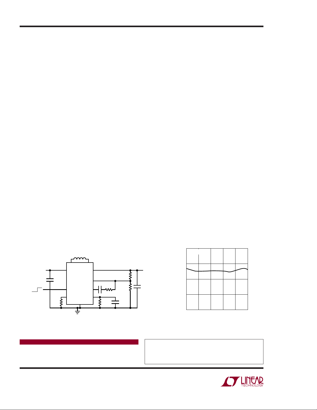
1.27mm Profi le Li-Ion to 3.3V Regulator
The high switching frequency and advanced buck-boost
switching algori thm of the LTC 3530 allow the use of small
external components. Figure 3 shows a circuit that is
optimized to reduce the total application size. The entire
converter h as a maximum height of 1.27mm and occupies
a PCB area of only 0.135 square inches making it ideal
for height constrained applications such as PC cards.
Figure 4 shows the effi ciency versus input voltage for
this area-optimized application circuit. This converter is
able to support a 600mA load for output voltages above
2.4V and obtains greater than 86% effi ciency over the
entire Li-Ion input voltage range.
Conclusion
The LTC3530 with its high effi ciency, wide input voltage
range, and tiny circuit size is well suited to a variety of
battery operated products and other effi ciency-sensitive applications. With the IC’s array of programmable
features, the circuit can be customized to meet the needs
of any application, while still maintaining a compact total
solution footprint.
L1
4.7µH
C
IN
10µF
SW1 SW2
V
SHDN/SS
R
V
IN
T
OUT
LTC3530
FB
V
C
BURST
GND
C
: MuRATA GRM21BR60J106K (0805 PACKAGE)
IN
: MuRATA GRM21BR60J226K (0805 PACKAGE)
C
OUT
L1: COOPER BUSSMAN SD12-2R2
330pF
100k
30.1k
340k
200k
DN413 F03
3V TO 4V
OFF ON
V
IN
33.2k 0.01µF
Figure 3. 1.27mm Profi le and Area Optimized Application Circuit
Data Sheet Download
http://www.linear.com
Linear Technology Corporation
1630 McCarthy Blvd., Milpitas, CA 95035-7417
●
(408) 432-1900
FAX: (408) 434-0507 ● www.linear.com
V
3.3V
650mA
C
OUT
22µF
OUT
94
I
= 150mA
OUT
90
86
EFFICIENCY (%)
82
78
3.2
3
INPUT VOLTAGE (V)
3.6
3.4
3.8
Figure 4. Effi ciency vs Input Voltage
of Figure 3 Circuit
For applications help,
call (408) 432-1900, Ext. 2759
dn413 LT/TP 0407 409K • PRINTED IN THE USA
© LINEAR TECHNOLOGY CORPORATION 2007
4
DN413 F04
 Loading...