

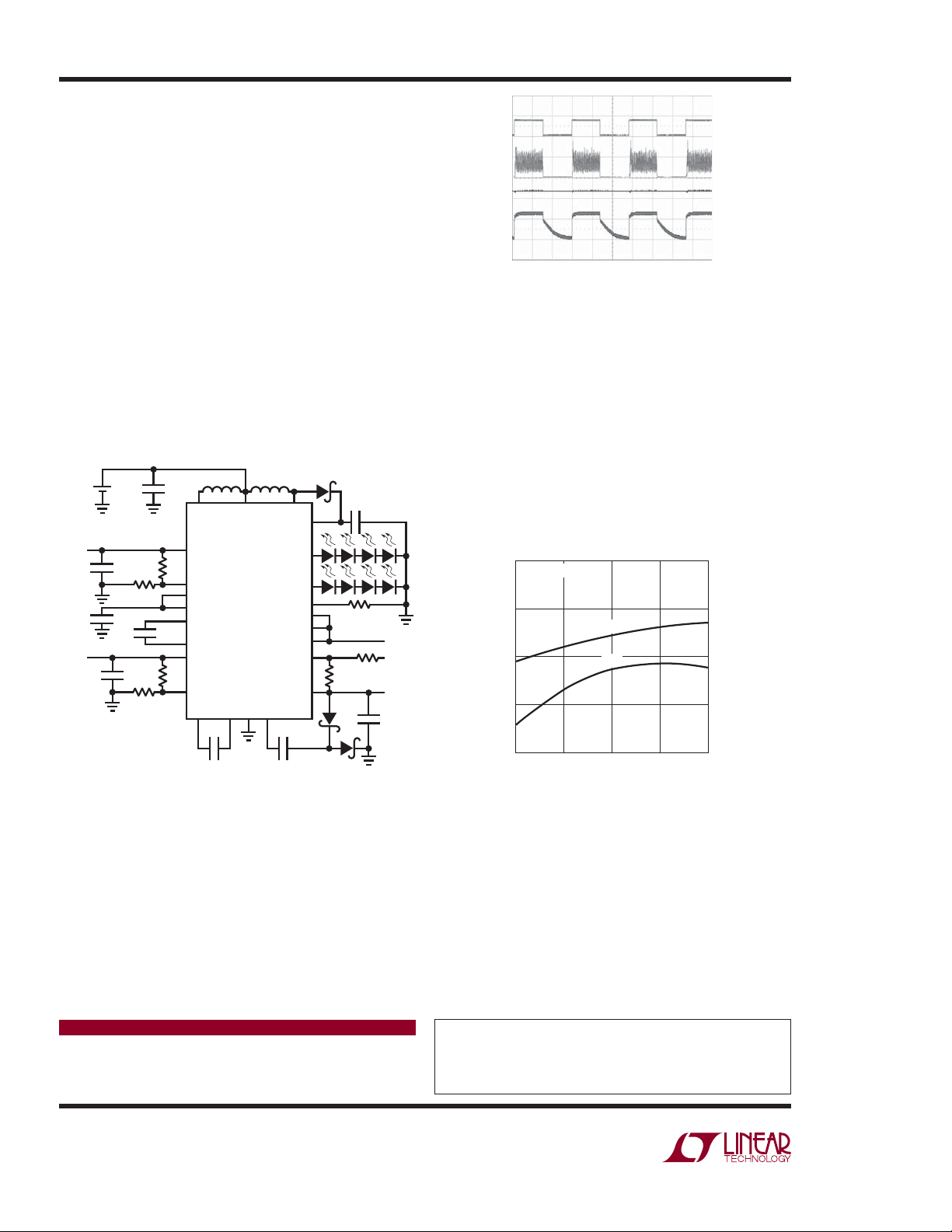
Versatile TFT LCD Bias Supply and White LED Driver
in a 4mm × 4mm QFN – Design Note 440
Eddy Wells
Introduction
The makers of h andheld medical, industrial and consumer
devices use a wide variety of high resolution, small to
medium sized color TFT LCD displays. The power supply
designers for these displays must contend with shrinking board area, tight schedules, and variations in display
®
type s and feature requirements. T he LTC
3524 simplifi es
the designer’s job by combining a versatile, easily programmed, TFT LCD bias supply and white LED backlight
driver in a low profi le 4mm × 4mm QFN package.
The LTC3524’s 2.5V to 6V input supply range is ideally
suited for portable devices powered from Li-Ion or
multiple alkaline or nickel cells. Both the LCD and LED
drivers operate at 1.5MHz, allowing the use of tiny, low
cost, inductors and capacitors.
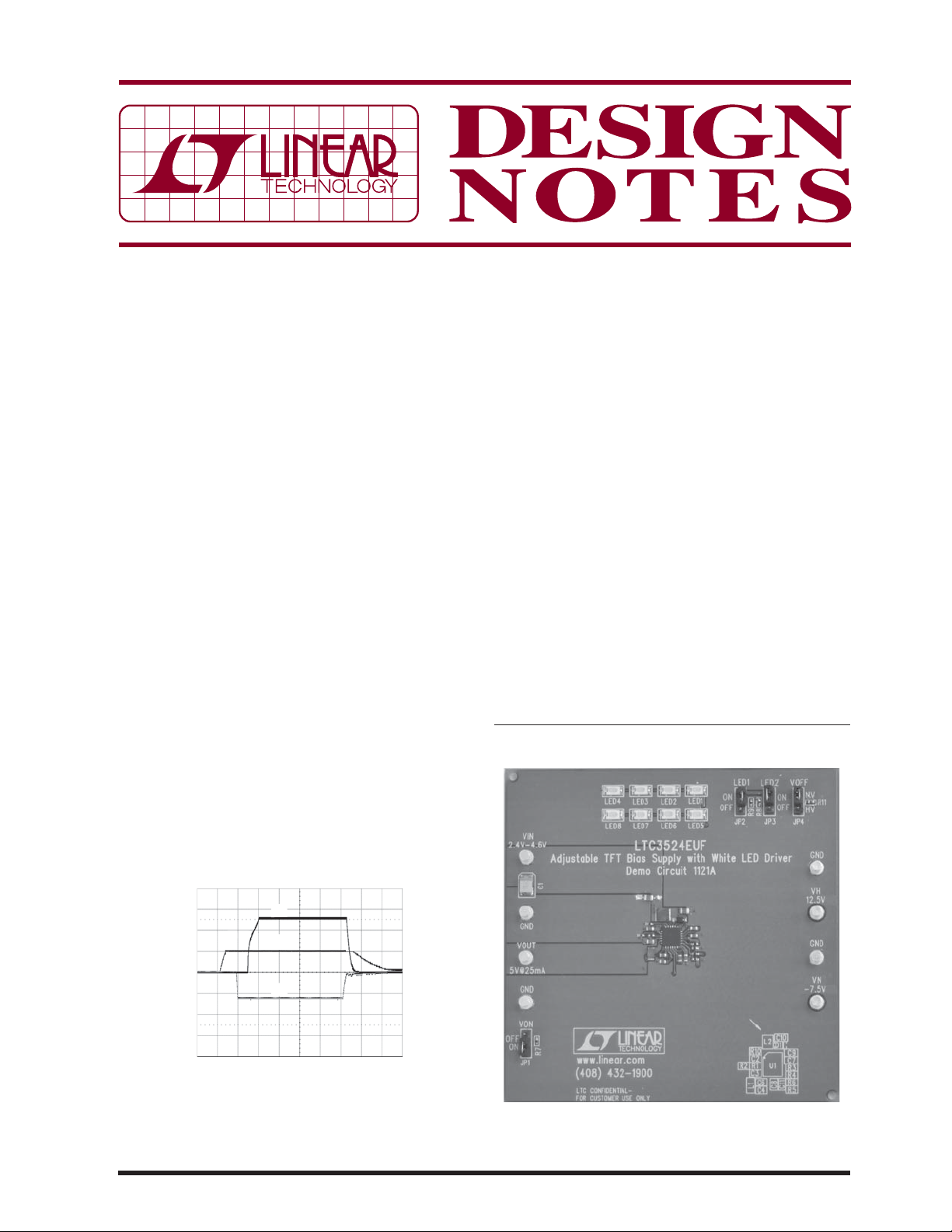
The TFT bias portion of the circuit consists of a synchronous boost converter, adjustable between 3V and
6V, providing the main analog V
for the TFT. Low
OUT
current gate drive voltages (VH and VN) are generated
using integrated charge-pump circuits. These low noise
outputs are pr ogrammable to ±20V, allowing optimal bias
for multiple display types and makers. The TFT outputs
are sequenced at power-up and dischar ged at power-down
as shown in Figure 1.
A second nonsynchronous boost converter gener ates the
voltage required to regulate one or two LED strings at
up to 25mA each. LED current can be adjusted by either
analog or digital means, optimizing the TFT display for
varying ambient light conditions. Each string is independently enabled and can contain 1 to 5 LEDs in series.
Internal circuitry maintains equal current in the strings,
even when the forward voltage drops of the LEDs do not
match. Open LED protection is provided to prevent the
output from exceeding 24V.
3-Output TFT Supply with Digitally Dimmed LED
Backlight
A LTC3524-based TFT and backlight solution for a 4 to 6
inch LCD is shown in Figure 2. High frequency operation
of the power components and the QFN package shrinks
the total converter footprint to approximately 120mm
2
(single sided).
L, LT, LTC and LTM are registered trademarks of Linear Technology Corporation.
All other trademarks are the property of their respective owners.
VH
V
OUT
5V/DIV
VN
5ms/DIV
Figure 1. LTC3524 TFT LCD Supply Sequencing
at Power-Up and Power-Down
05/08/440
DN4EW F01
DN4EW F02
Figure 2. LTC3524-Based LCD and White LED Supply
The circuit schematic is shown in Figure 3. The TFT bias
portion of the circuit provides a 5V, 25mA output for the
TFT drivers as well as 12.5V and –7.5V outputs with up
to 2mA for the gate bias. These voltages are programmed
using the FBVO, FBH, and FBN pins respectively.
As shown in Figure 1, these outputs are sequenced with
, V N , t h e n V H p o w e r e d , a s r e q u i r e d b y m o s t d i s p l a y s .
V
OUT
The output s are actively discharged w hen ELCD is brought
low, removing voltage from the display.
The white LED backlight for the Figure 3 circuit consists
of two strings with four series LEDs. The LEDs are
driven from the high side with the LTC3524, allowing the
strings to terminate at ground, reducing the number of
wires required to power the display. With R
PROG
= 100k,
each LED is regulated to 20mA. Maximum power for the
backlight is approximately 600mW, assuming a forward
voltage around 3.6V per element.
25mA
12.5V
2mA
+
Li-Ion
–
5V
10μF
10V
0.47μF
324k
0.47μF
220k
0.1μF
2.2μF
1M
2M
SW1
V
OUT
FBVO
VNIN
V2x
2
C
C2
VH
FBH
CH
+
–
+
0.1μF
Figure 3. Complete TFT and LED Solution
CH
IN
LTC3524
–
GND
3.3μH10μH
SW2V
VLED
LED2
LED1
PROG
ELED2
ELED1
ELCD
FBN
VN
+
C
N
0.1μF
10μF
100k for 20mA
470k
1M
DN4EW F03
V
IN
V
OUT
–7.5V
2mA
0.47μF
E
AND
LED1
E
LED2
I
BOOST
LED
INDUCTOR
V
LED2
LED
12.5V
12V
500μs/DIV
5V/DIV
200mA/DIV
10V/DIV
10V/DIV
DN4EW F04
Figure 4. Burst Dimming Waveforms
Effi ciency results for this design are given in Figure 5
with a 3.6V input. The LCD effi ciency curve shows the
performance of the synchronous boost converter with
at 5V and varying load current. This curve includes
V
OUT
the no load quiescen t current of the ch arge-pumps, which
are powered from V
OUT
.
Analog dimming of the LEDs can be implemented by
adjusting the current through the PROG pin. Effi ciency
for analog dimming is shown in Figure 5. Effi ciency with
PWM dimming would remain close to 78% over a wide
dimming range.
100
VIN = 3.6V
90
LCD
80
EFFICIENCY (%)
70
60
5
V
OUT
OR LED STRING CURRENT (mA)
LED
10
15
20
25
DN4EW F05
Dimming is achieved by changing the duty cycle of a 200Hz
power signal applied to the LED strings. The frequency is
high enough to prevent visually detectable fl ickering, but
low enough to allow a better than 100:1 dimming range.
Dimming is implemented by simply connecting a microprocessor controlled port to ELED1 and ELED2. Scope
waveforms at 50% duty cycle are shown in Figure 4.
Data Sheet Download
www.linear.com
Linear Technology Corporation
1630 McCarthy Blvd., Milpitas, CA 95035-7417
●
(408) 432-1900
FAX: (408) 434-0507 ● www.linear.com
Figure 5. LCD Bias and LED Effi ciency
Conclusion
The LTC3524 shrinks and simplifi es the design of small
to medium sized TFT LCDs by combining the LCD supply
and LED driver in a single compact package. LCD bias
voltages and LED currents are programmable, making
it possible to simplify parts stock by using the LTC3524
for a wide variety of displays.
For applications help,
call (408) 432-1900, Ext. 3222
dn440f LT/TP 0508 246K • PRINTED IN THE USA
© LINEAR TECHNOLOGY CORPORATION 2008
 Loading...