


FEATURES
■
350mA Constant Current Output
■
2.8V to 4V Output Compliance
■
1- or 2-Cell NiMH or Alkaline Input
■
Synchronous Rectification: Up to 90% Efficiency
■
Fixed Frequency Operation: 1.3MHz
■
Low Quiescent Current: <1mA
■
Very Low Shutdown Current: <50µA
■
Open LED Output Limited to 4.7V
■
VIN Range: 1V to 3.2V
■
Dimming Control
■
Undervoltage Lockout to Protect Batteries
■
Low Profile (0.75mm) 3mm × 3mm Thermally
Enhanced 8-Lead DD and S8 Packages
U
APPLICATIO S
■
Portable Lighting
■
Rechargeable Flashlights
LTC3490
Single Cell 350mA
LED Driver
U
DESCRIPTIO
The LTC®3490 provides a constant current drive for 1W
LED applications. It is a high efficiency boost converter
that operates from 1 or 2 NiMH or alkaline cells and
generates 350mA of constant current with up to 4V of
compliance. It contains a 100mΩ NFET switch and a
130mΩ PFET synchronous rectifier. The fixed switching
frequency is internally set to 1.3MHz.
The LTC3490 limits the output voltage to 4.7V if the output
load is disconnected. It also features an analog dimming
capability that reduces the drive current proportional to
the CTRL/SHDN pin voltage. A low-battery logic output
signals when the battery has dropped below 1V/cell. An
undervoltage lockout circuit shuts down the LTC3490
when the battery voltage drops below 0.85V/cell. The
feedback loop is internally compensated to minimize component count.
, LT, LTC and LTM are registered trademarks of Linear Technology Corporation.
All other trademarks are the property of their respective owners.
TYPICAL APPLICATIO
Single Cell Minimum Component LED Driver
3.3µH
V
IN
1 NiMH OR
ALKALINE
CELL
ON/OFF
+
1M
LTC3490
CTRL/SHDN
CELLS
GND
LOBAT
SW
CAP
LED
U
350mA
4.7µF
HIGH
CURRENT
LED
3490 TA01
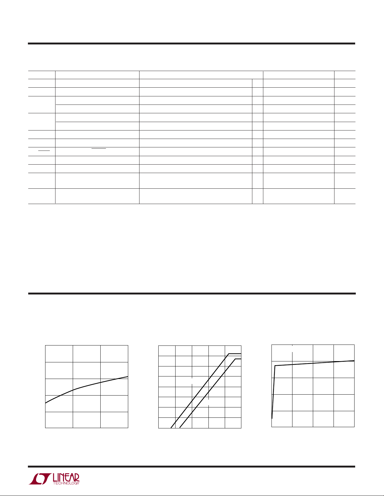
Efficiency vs V
100
I
= 350mA
OUT
90
80
70
60
50
40
EFFICIENCY (%)
30
20
10
0
1
1.5
IN
2
VIN (V)
at V
LED
= 3.5V
2.5
3
3490 TA02
3490fa
1
LTC3490
WWWU
ABSOLUTE AXI U RATI GS
(Note 1)
Supply Voltage (VIN) ................................... –0.3V to 6V
Input Voltages (CTRL/SHDN, CELLS) ......... – 0.3V to 6V
Output Voltages (CAP, LED, SW)................ – 0.3V to 6V
/
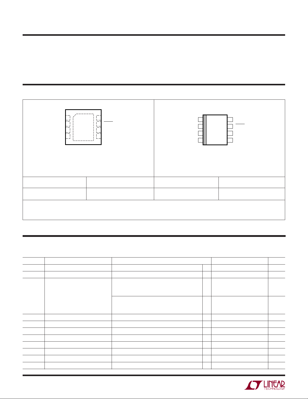
PACKAGE
O
RDER I FOR ATIO
1CELLS
V
2
IN
SW
3
GND
4
8-LEAD (3mm × 3mm) PLASTIC DFN
T
= 125°C, θJA = 43°C/ W (NOTE 4)
JMAX
EXPOSED PAD (PIN 9) IS GND
MUST BE SOLDERED TO PCB (NOTE 5)
ORDER PART NUMBER
LTC3490EDD
TOP VIEW
9
DD PACKAGE
WU
8
CTRL/SHDN
LOBAT
7
CAP
6
LED
5
DD PART MARKING
LBRQ
U
Operating Temperature Range (Note 2) .. –40°C to 85°C
Storage Temperature Range ................. –65°C to 125°C
Lead Temperature (Soldering, 10 sec, S8) .......... 300°C
TOP VIEW
CELLS
1
V
2
IN
SW
3
GND
4
S8 PACKAGE
8-LEAD PLASTIC SO
T
= 125°C, θJA = 150°C/ W (NOTE 4)
JMAX
CTRL/SHDN
8
LOBAT
7
CAP
6
LED
5
ORDER PART NUMBER S8 PART MARKING
LTC3490ES8
3490
Order Options
Lead Free: Add #PBF Lead Free Tape and Reel: Add #TRPBF
Lead Free Part Marking: http://www.linear.com/leadfree/
Consult LTC Marketing for parts specified with wider operating temperature ranges.
ELECTRICAL CHARACTERISTICS
Tape and Reel: Add #TR
The ● denotes specifications which apply over the full operating
temperature range, otherwise specifications are TA = 25°C. VIN = 2.5V unless otherwise specified.
SYMBOL PARAMETER CONDITIONS MIN TYP MAX UNITS
V
IN
V
IN(START)
I
LED(MAX)
I
LED(SHDN)
V
LED
V
LED(OVL)
I
IN(SHDN)
I
IN(ACTIVE)
f
SW
I
L(NMOS)
R
ON(NMOS)
Input Supply Range 1 3.2 V
Minimum Start-Up Voltage (Note 3) 0.9 1 V
LED Drive Current V
LED Drive Current in Shutdown V
Output Compliance Voltage
Output Voltage Overvoltage Limit Open LED
Input Current, Shutdown V
Input Current, Active Excluding Load Power 20 30 mA
Switching Frequency
Leakage Current, NMOS Switch 0.1 µA
On-Resistance, NMOS Switch 0.1 Ω
CTRL/SHDN
25°C to 85°C 330 350 370 mA
–40°C to <25°C 310 350 385 mA
V
CTRL/SHDN
25°C to 85°C 337 350 363 mA
–40°C to <25°C 325 345 365 mA
CTRL/SHDN
CTRL/SHDN
= VIN, DD Package
= VIN, S8 Package
= 0V 0.1 1 µA
●
2.8 4 V
●
4.2 4.7 V
= 0V, Excluding Switch Leakage 20 50 µA
●
1.0 1.3 1.6 MHz
3490fa
2
LTC3490
ELECTRICAL CHARACTERISTICS
temperature range, otherwise specifications are T
A
The ● denotes specifications which apply over the full operating
= 25°C. VIN = 2.5V unless otherwise specified.
SYMBOL PARAMETER CONDITIONS MIN TYP MAX UNITS
I
L(PMOS)
R
ON(PMOS)
V
IH
Leakage Current, PMOS Switch 0.1 µA
On-Resistance, PMOS Switch 0.13 Ω
Input High (CELLS) VIN – 0.4 V
Input High (SHDN) VIN • 0.9 V
V
IL
Input Low (CELLS) 0.4 V
Input Low (SHDN) VIN • 0.2 V
I
IN
K
CTRL
R
ON(LOBAT)
V
IN(LOBAT1)
V
IN(LOBAT2)
V
IN(UVLO2)
Input Current (CTRL/SHDN, CELLS) 0.01 µA
Control Gain, I
LED/VCTRL
On-Resistance, LOBAT Output VIN < V
Input Voltage, Low Battery, 1 Cell V
Input Voltage, Low Battery, 2 Cells V
Input Voltage, Undervoltage Lockout, V
Scales Linearity with VIN, VIN = 1V 500 mA/V
CELLS
CELLS
CELLS
IN(LOBAT)
= 0V
= V
IN
= V
IN
●
●
0.8 1.12 V
●
1.8 2.24 V
●
1.4 1.8 V
300 Ω
2 Cells
V
IN(UVLO1)
Input Voltage, Undervoltage Lockout, V
CELLS
= 0 V
●
0.7 0.9 V
1 Cell
Note 1: Stresses beyond those listed under Absolute Maximum Ratings
may cause permanent damage to the device. Exposure to any Absolute
Maximum Rating condition for extended periods may affect device
reliability and lifetime.
Note 2: The LTC3490 is guaranteed to meet performance specifications
from 0°C to 70°C. Specifications over the –40°C to 85°C range are
assured by design, characterization and correlation with statistical process
controls.
Note 4: This device includes overtemperature protection intended to
protect the device during momentary overload conditions. The maximum
junction temperature may be exceeded when overtemperature protection
is active. Continuous operation above the specified maximum operating
junction temperature may result in device degradation or failure.
Note 5: The Exposed Pad of the DFN package must be soldered to a
PCB pad for optimum thermal conductivity. This pad must be connected
to ground.
Note 3: The LTC3490 input voltage may drop below the minimum start-up
voltage once the LED voltage has risen above 2.3V.
UW
TYPICAL PERFOR A CE CHARACTERISTICS
Oscillator Frequency
vs V
400
350
300
250
(mA)
200
LED
I
150
100
I
LED
50
0
0
CTRL
MAXIMUM
MINIMUM
0.2 0.4 0.8
V
CTRL/VIN
0.6
(V)
vs Temperature
1.400
1.360
1.320
1.280
FREQUENCY (MHz)
1.240
1.200
–50
0
TEMPERATURE (°C)
50
100
3490 G01
3490 G02
I
vs V
LED
375
350
325
(mA)
LED
I
300
275
250
1
1
IN
V
= 3.5V
LED
1.5
2
VIN (V)
2.5
3
3490 G03
3490fa
3
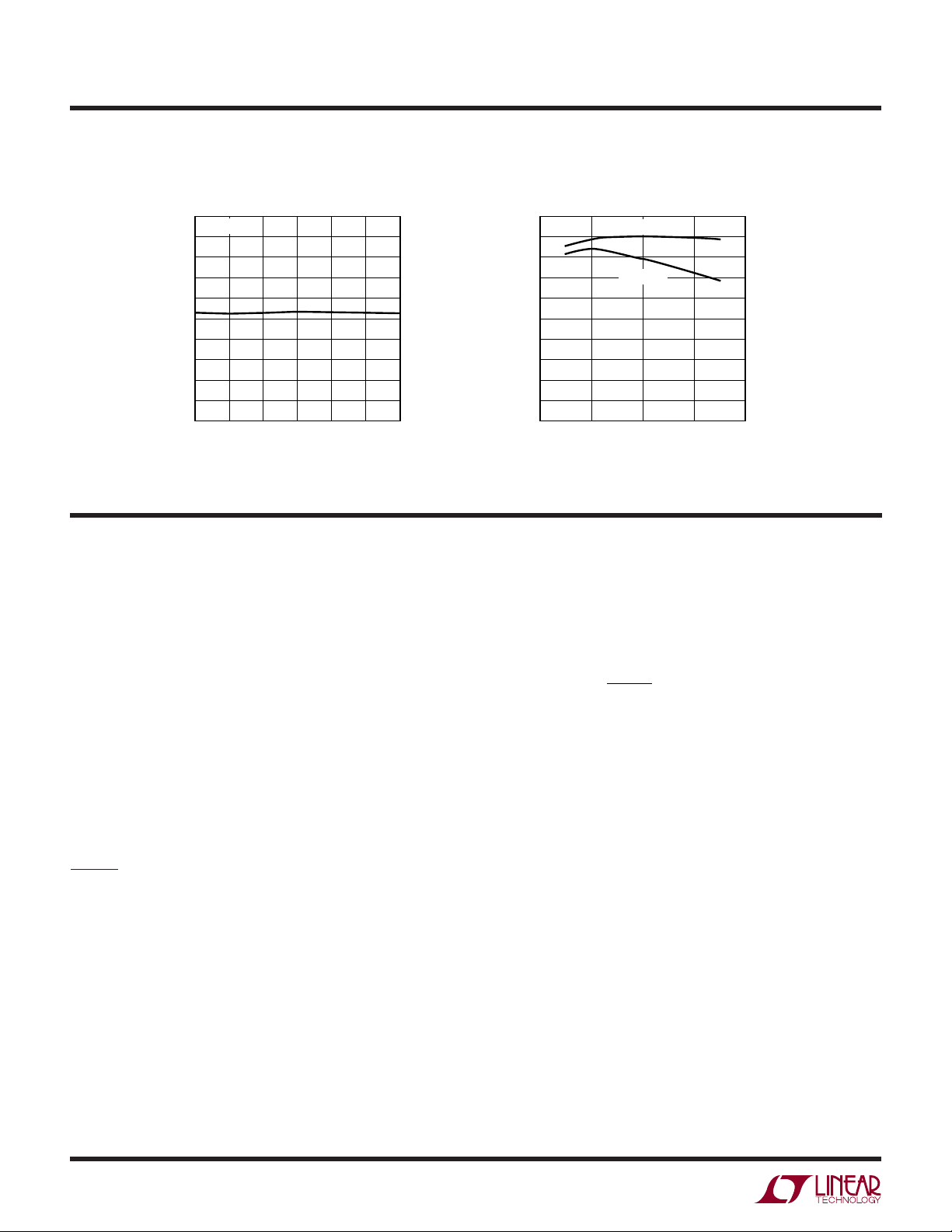
LTC3490
I
LED
(mA)
0
0
EFFICIENCY (%)
10
30
40
50
100
70
100
200
3490 G05
20
80
90
60
300
400
VIN = 2.4V
VIN = 1.2V
UW
TYPICAL PERFOR A CE CHARACTERISTICS
I
360
358
356
354
352
(mA)
350
LED
I
348
346
344
342
340
LED
VIN = 2.4V
2.8
vs V
3 3.2
LED
3.4 3.6 3.8
V
(V)
LED
4
3490 G04
Efficiency vs I
LED
PI FU CTIO S
U
UU
CELLS (Pin 1): A logic input to set the low-battery and
undervoltage shutdown thresholds. A logic low (tied to
GND) will set the thresholds for 1 cell. A logic high (tied to
VIN) will set the thresholds for 2 cells.
(Pin 2): Supply Voltage.
V
IN
SW (Pin 3): Switch Input. Connect this pin to an external
inductor from V
IN
.
GND (Pin 4): Circuit Ground.
LED (Pin 5): Output Drive Current to LED.
CAP (Pin 6): Filter Capacitor. A 4.7µF low ESR capacitor
should be tied to this pin.
LOBAT (Pin 7): Low active, open-drain logic output indicating a low-battery condition.
4
CTRL/SHDN (Pin 8): Analog Control Voltage and Shutdown. When V
• 0.2 < V
IN
< VIN • 0.9, the LED drive
CTRL
current varies according to the formula:
⎛
I
LED
When V
500 0 2•–.
=
CTRL
V
⎜
⎝
> VIN • 0.9, the LED drive current is clamped
at 350mA. When V
CTRL
V
IN
CTRL
⎞
mA
⎟
⎠
< VIN • 0.2, then the part is in low
power shutdown.
Exposed Pad (Pin 9, DD Package): Ground. This pin must
be soldered to the PCB to provide both electrical contact
to ground and good thermal contact to the PCB.
3490fa

LTC3490
U
U
W
FU CTIO AL DIAGRA
–
V
IN
2
+
GATE
CONTROL
DRIVERS
PWM
LOGIC
START-UP
AND
LIMIT
P BODY
CONTROL
OSCILLATOR
3
SW
SENSE
OVERVOLTAGE
DETECT
AMP
CAP
6
0.1Ω
19.2Ω
+
–
250k
LED
5
–
+
V
/2
REF
40k
8
1
CTRL/
SHDN
CELLS
DIMMING
–
AMP
+
I
REF
GND
4
BATTERY
MONITOR
SHUTDOWN
LOBAT
7
3490 FD
3490fa
5

LTC3490
OPERATIO
U
The LTC3490 is a high efficiency, constant current source
for 1W high intensity white LEDs. These high intensity
LEDs require a fixed current of 350mA with a voltage
compliance of 2.8V to 4V.
The LTC3490 operates with 1 or 2 NiMH or alkaline cells.
It functions as a boost converter with a current sense resistor providing the control feedback. If the battery voltage
is greater than the required LED compliance, it will cycle
off periodically to maintain the correct average current. It
features a low voltage start-up circuit that will start with an
input voltage of only 1V. Once the drive voltage exceeds
2.3V, the circuit operates from the drive voltage.
All of the loop compensation is internal; only the main filter
capacitor is needed for stable operation.
Dimming Function
During normal operation with the CTRL/SHDN pin connected to V
350mA. The drive current can be reduced by changing the
voltage on the CTRL/SHDN pin.
For VIN • 0.2 < V
proportional to V
ometer from V
, the LED drive current is controlled at
IN
< VIN • 0.9, the LED current is
CTRL
CTRL/VIN
to control the current without sensitivity
IN
. This allows a simple potenti-
to the battery voltage. The LED drive current is given by the
formula:
⎛
V
500 0 2•–.
I
=
LED
When V
at 350mA.
Open-Circuit Protection
Since this is a boost converter attempting to drive a current into the load, an open or high impedance load will cause
the regulator loop to increase the output voltage in an effort to achieve regulation. To protect the device, maximum
output voltage is limited to 4.7V under all conditions.
Undervoltage Sense and Protection
The undervoltage lockout prevents excessive inductor
peak current and protects the batteries from deep discharging which can damage them. The low-battery indicator allows the end user to be made aware that the batteries
are nearing the end of their useful life.
CTRL
CTRL
⎜
⎝
V
IN
> VIN • 0.9, the LED drive current is clamped
⎞
⎟
⎠
mA
6
3490fa

WUUU
APPLICATIO S I FOR ATIO
LTC3490
The LTC3490 requires only four external components to
operate: an inductor, an output capacitor, a switch and a
pull-down resistor. The inductor is nominally set at 3.3µH
and the capacitor at 4.7µF. Optional components include
an input capacitor and dimming resistors.
COMPONENT SELECTION
Inductor Selection
The high frequency operation of the LTC3490 allows the
use of small surface mount inductors. The minimum
inductance value is proportional to the operating frequency and is limited by the following constraints:
3
LfH
≥
and
VV V
IN MIN OUT MAX IN MIN
≥
L
•–
() ( ) ()
()
••
f Ripple V
OUT MAX
()
H
where:
f = Operating Frequency (Hz)
Ripple = Inductor Current Ripple (A)
V
V
= Minimum Input Voltage (V)
IN(MIN)
OUT(MAX)
= Maximum Output Voltage (V)
The inductor current ripple is typically set to 20% to 40%
of the inductor current.
The peak inductor current is given by:
where:
= Input Voltage (V)
V
IN
= Output Voltage (V)
V
OUT
I
= LED Drive Current (A)
OUT
= Input Current = V
I
IN
= R
R
P
R
= R
N
of the PFET Switch (Ω)
DSON
of the NFET Switch (Ω)
DSON
OUT/VIN
• I
OUT
(A)
For high efficiency, choose an inductor with a high frequency core material, such as ferrite, to reduce core
losses. The inductor should have low ESR (equivalent
2
series resistance) to reduce the I
R losses and must be
able to handle the peak inductor current at full load without
saturating. In single cell applications, the inductor ESR
must be below 25mΩ to keep the efficiency up and
maintain output current regulation. Dual cell applications
can tolerate significantly higher ESR (up to 75mΩ) with
minimal efficiency degradation. Molded chokes or chip
inductors usually do not have enough core to support the
peak inductor currents in the 1A to 2A region. If radiated
noise is an issue, use a toroid, pot core or shielded bobbin
inductor to minimize radiated noise. See Table 1 for a list
of suggested inductors. Look closely at the manufacturers
data sheets; they specify saturation current differently.
Table 1. Inductor Information
INDUCTOR PART NUMBER ESR (mΩ) SATURATION CURRENT (A)
TOKO A918CY-3R3M 47 1.97
TYCO DN4835-3R3M 58 2.15
TDK SLF7045T-3R3M2R5 20 2.5
II
=
LPK OUT
()
+
VIRRI
+
OUT OUT P N IN
VV V
()
IN OUT IN
•••2
LfV
•–•
–•
VRI
IN N IN
–
OUT
Output Capacitor Selection
The output capacitor value and equivalent series resistance (ESR) are the primary factors in the output ripple.
The output ripple is not a direct concern for LED drive as
the LED will operate at the average current value. However
the peak pulsed forward current rating of the LED must not
be exceeded to avoid damaging the LED.
3490fa
7

LTC3490
WUUU
APPLICATIO S I FOR ATIO
The output ripple voltage has two primary components.
The first is due to the value of the capacitor and is given by:
IV
•
VR
CAP
LPK IN
=
CV f
••
OUT
The second is due to the capacitor ESR:
VR
= I
LPK
• R
ESR
ESR
The LED current ripple and peak pulsed current are calculated by:
IR
LED
II
PPFC OUT
VR VR
=
RR
=+
•
CAP ESR
IR
+
LE
DD
SENSE LED
2
where:
R
R
= Internal Sense Resistor = 0.1Ω
SENSE
= Dynamic Impedance of the LED
LED
Component values will be calculated for 1 or 2 NiMH cells
and assumes the end-of-charge voltage to be 0.9V per cell.
The operating frequency is assumed to be 1MHz, the
worst-case low frequency. The allowed inductor ripple
current is 0.31A. Table 3 shows a summary of the key
parameters.
Table 3. Summary of Key Parameters
PARAMETER 1-CELL 2-CELL UNITS
L
MIN
Choose L 3.3 3.3 µH
I
IN
I
LPK
Choose C 4.7 4.7 µF
Cap ESR 5 5 mΩ
VR
CAP
VR
ESR
IR
LED
I
PPFC
2.2 3.2 µH
1.56 0.78 A
1.93 0.96 A
0.09 0.09 V
0.01 0.005 V
0.10 0.09 A
0.40 0.39 A
where:
Low ESR capacitors should be used to minimize output
ripple. Ceramic X5R or X7R type capacitors are recommended. See Table 2 for a list of component suppliers.
Table 2. Capacitor Information
CAPACITOR PART NUMBER DESCRIPTION
TDK C2012X5R0J475K 4.7µF, 6.3V, X5R in 0805
AVX 1210ZC475MAT 4.7µF, 10V, X7R in 1210
Taiyo Yuden CELMK316BJ475ML 4.7µF, 10V, X7R in 1206
Input Capacitor Selection
Most battery-powered applications do not need an input
capacitor. In supply-powered applications or battery applications with long leads to the battery, a low ESR 3.3µF
capacitor reduces switching noise and peak currents.
Design Example
The example will use a Lumileds DS25 white LED. The key
specifications are:
V
(at IF= 350mA) = 3.4 ±0.6V
F
I
is the peak inductor current
LPK
VR
is the ripple voltage due to the output capacitor
CAP
value
is the ripple voltage due to the output capacitor
VR
ESR
ESR
is the LED current ripple
IR
LED
I
is the LED peak pulsed forward current
PPFC
PC Board Layout Checklist
Keep the inductor and output capacitor as close to the IC
as possible. Make traces as short and wide as is feasible.
Parasitic resistance and inductance reduce efficiency and
increase ripple.
Keep resistance in the battery connections as low as
possible. In single cell applications, only 0.1Ω in the
battery connections will have a dramatic effect in efficiency and battery life. I2R losses can exceed 100mW and
the converter operates lower on the efficiency curve.
R
= 1Ω
LED
Peak Pulsed Forward Current = 0.5A
8
3490fa

WUUU
APPLICATIO S I FOR ATIO
LTC3490
Red Luxeon LEDs
The red, red-orange and amber Luxeon LEDs have a lower
forward voltage than the white, blue and green LEDs. Since
the LTC3490 internal circuitry is powered from the output,
it requires a minimum LED voltage of 2.5V for reliable
operation. The minimum forward voltage on the red LEDs
U
TYPICAL APPLICATIO S
2-Cell Adjustable Amplitude LED Driver
3.3µH
V
IN
LTC3490
CTRL/SHDN
CELLS
GND
2 NiMH OR
ALKALINE
CELLS
ON/OFF
+
+
1M
is only 2.31V. The LTC3490 requires an additional 190mV
for proper operation. In non-dimming applications, this can
be accomplished with a 0.6Ω resistor in series with the
LED. The resistor voltage drops too low in dimming applications, so a Schottky diode is recommended to keep
sufficient voltage at the output at lower currents.
SW
CAP
LED
LOBAT
4.7µF
LUMILEDS
LUXEON
LXHL-BW02
1 NiMH OR
ALKALINE
CELL
3490 TA03
Soft Turn-Off LED Driver
3.3µH
LTC3490
GND
SW
CAP
LED
LOBAT
350mA
4.7µF
LUMILEDS
LUXEON
LXHL-BW02
3490 TA04
V
IN
ON/OFF
+
CTRL/SHDN
1µF
1M
CELLS
3490fa
9

LTC3490
U
TYPICAL APPLICATIO S
Luxeon Red LED Driver Without Dimming
3.3µH
1 NiMH OR
ALKALINE
CELL
1 NiMH OR
ALKALINE
CELL
ON/OFF
V
IN
+
CTRL/SHDN
1M
CELLS
LTC3490
GND
SW
CAP
LED
LOBAT
0.6Ω
4.7µF
LUMILEDS
LUXEON
LXHL-BD03
3490 TA06
Luxeon Red LED Driver with Dimming
3.3µH
ON/OFF
V
IN
+
1M
CTRL/SHDN
CELLS
LTC3490
GND
SW
CAP
LED
LOBAT
4.7µF
MBRM120E
LUMILEDS
LUXEON
LXHL-BD03
3490 TA07
10
Efficiency vs VIN with Red LED
90
80
70
60
50
40
EFFICIENCY (%)
30
20
10
0
1
RESISTOR
1.5
2
VIN (V)
SCHOTTKY
2.5
3
3490 G06
3490fa

PACKAGE DESCRIPTIO
U
DD Package
8-Lead Plastic DFN (3mm × 3mm)
(Reference LTC DWG # 05-08-1698)
0.675 ±0.05
R = 0.115
TYP
LTC3490
0.38 ± 0.10
85
3.5 ±0.05
1.65 ±0.05
(2 SIDES)2.15 ±0.05
PACKAGE
OUTLINE
0.25 ± 0.05
RECOMMENDED SOLDER PAD PITCH AND DIMENSIONS
2.38 ±0.05
(2 SIDES)
0.50
BSC
8-Lead Plastic Small Outline (Narrow .150 Inch)
.050 BSC
PIN 1
TOP MARK
(NOTE 6)
0.200 REF
NOTE:
1. DRAWING TO BE MADE A JEDEC PACKAGE OUTLINE M0-229 VARIATION OF (WEED-1)
2. DRAWING NOT TO SCALE
3. ALL DIMENSIONS ARE IN MILLIMETERS
4. DIMENSIONS OF EXPOSED PAD ON BOTTOM OF PACKAGE DO NOT INCLUDE
MOLD FLASH. MOLD FLASH, IF PRESENT, SHALL NOT EXCEED 0.15mm ON ANY SIDE
5. EXPOSED PAD SHALL BE SOLDER PLATED
6. SHADED AREA IS ONLY A REFERENCE FOR PIN 1 LOCATION
ON TOP AND BOTTOM OF PACKAGE
S8 Package
(Reference LTC DWG # 05-08-1610)
.045 ±.005
8
3.00 ±0.10
(4 SIDES)
0.75 ±0.05
0.00 – 0.05
.189 – .197
(4.801 – 5.004)
NOTE 3
7
6
1.65 ± 0.10
(2 SIDES)
5
0.25 ± 0.05
2.38 ±0.10
(2 SIDES)
BOTTOM VIEW—EXPOSED PAD
14
0.50 BSC
(DD8) DFN 1203
.245
MIN
.030
±
.005
TYP
RECOMMENDED SOLDER PAD LAYOUT
.010 – .020
(0.254 – 0.508)
.008 – .010
(0.203 – 0.254)
NOTE:
1. DIMENSIONS IN
2. DRAWING NOT TO SCALE
3. THESE DIMENSIONS DO NOT INCLUDE MOLD FLASH OR PROTRUSIONS.
MOLD FLASH OR PROTRUSIONS SHALL NOT EXCEED .006" (0.15mm)
Information furnished by Linear Technology Corporation is believed to be accurate and reliable.
However, no responsibility is assumed for its use. Linear Technology Corporation makes no representation that the interconnection of its circuits as described herein will not infringe on existing patent rights.
× 45°
.016 – .050
(0.406 – 1.270)
INCHES
(MILLIMETERS)
.160
±
.005
0°– 8° TYP
.228 – .244
(5.791 – 6.197)
.053 – .069
(1.346 – 1.752)
.014 – .019
(0.355 – 0.483)
TYP
.150 – .157
(3.810 – 3.988)
NOTE 3
1
3
2
4
.004 – .010
(0.101 – 0.254)
.050
(1.270)
BSC
SO8 0303
3490fa
11

LTC3490
TYPICAL APPLICATIO
U
LED Driver Drops to 20% Amplitude on Low-Battery Detect
3.3µH
1 NiMH OR
ALKALINE
CELL
ON/OFF
1M
1M
432k
+
V
IN
CTRL/SHDN
CELLS
LTC3490
GND
SW
CAP
350mA/70mA
LED
LOBAT
RELATED PARTS
PART NUMBER DESCRIPTION COMMENTS
LT®1618 Constant Current, Constant Voltage 1.4MHz, VIN: 1.6V to 18V, V
High Efficiency Boost Regulator Packages
LT1932 Constant Current, 1.2MHz, High Efficiency White VIN: 1V to 10V, V
LED Boost Regulator
LT1937 Constant Current, 1.2MHz, High Efficiency White VIN: 2.5V to 10V, V
LED Boost Regulator Packages
LTC3205 High Efficiency, Multi-Display LED Controller VIN: 2.8V to 4.5V, V
LTC3216 1A Low Noise, High Current LED Charge Pump with VIN: 2.9V to 4.4V, V
Independent Flash/Torch Current Control
LTC3402 2A, 3MHz Micropower Synchronous Boost Converter VIN: 0.85V to 5V, V
MS/EDD Packages
LTC3453 500mA Synchronous Buck-Boost High Current LED VIN: 2.7V to 5.5V, V
Driver in QFN
LT3465/LT3465A Constant Current, 1.2MHz/2.7MHz, High Efficiency VIN: 2.7V to 16V, V
White LED Boost Regulator with Integrated Schottky
Diode
LT3466 Dual Constant Current, 2MHz, High Efficiency VIN: 2.7V to 24V, V
White LED Boost Regulator with Integrated Schottky
Diode
LT3479 3A, Full-Featured DC/DC Converter with Soft-Start VIN: 2.5V to 24V, V
and Inrush Current Protection Packages
ThinSOT is a trademark of Linear Technology Corporation.
OUT(MAX)
4.7µF
LUMILEDS
LUXEON
LXHL-BWO2
3490 TA05
= 34V, IQ = 1.8mA, ISD < 1µA, MS/EDD
OUT(MAX)
= 34V, IQ = 1.2mA, ISD < 1µA, ThinSOT Packages
= 34V, IQ = 1.9mA, ISD < 1µA, ThinSOTTM/SC70
OUT(MAX)
= 6V, IQ = 50µA, ISD < 1µA, QFN24 Package
OUT(MAX)
= 5.5V, IQ = 300µA, ISD < 2.5µA, DFN Package
OUT(MAX)
= 5V, IQ = < 38µA, ISD < 1µA,
OUT(MAX)
= 5.5V, IQ = 0.6mA, ISD < 6µA, QFN Package
OUT(MAX)
= 34V, IQ = 1.9mA, ISD < 1µA, ThinSOT Package
OUT(MAX)
= 40V, IQ = 5mA, ISD < 16µA, DFN Package
OUT(MAX)
= 40V, IQ = 6.5mA, ISD < 1µA, DFN/TSSOP
OUT(MAX)
12
Linear Technology Corporation
1630 McCarthy Blvd., Milpitas, CA 95035-7417
(408) 432-1900 ● FAX: (408) 434-0507
●
www.linear.com
3490fa
LT 0606 REV A • PRINTED IN THE USA
© LINEAR TECHNOLOGY CORPORATION 2005
 Loading...