

Page 1
advertisement
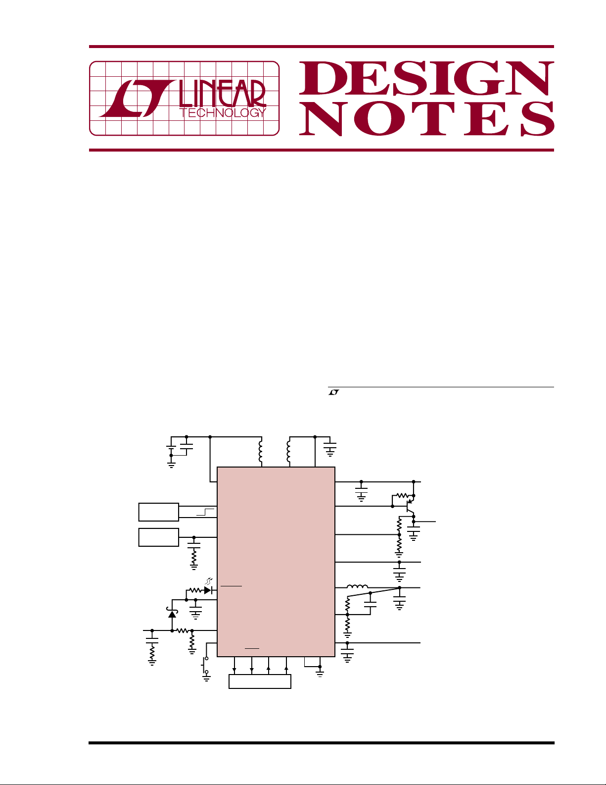
Multiple Output DC/DC Converter Runs Off 2-Cell AA Batteries,
USB or AC Wall Adapter
– Design Note 1006
Gurjit Ghandi and Minjong Kim
Introduction
The LTC®3456 is a low profile, total power management
solution optimized for the confined spaces and diverse
power requirements of mobile devices, including MP3
players, portable GPS units, digital cameras and handheld
computers. The LTC3456 seamlessly manages power
flow between an AC adapter, USB cable and a 2-cell AA
battery while complying with USB power standards and
fits in a 4mm × 4mm 24-pin QFN package.
The device generates two separate power rails: a 3.3V
(fixed) main supply and a 1.8V (adjustable) core supply.
In addition, the LTC3456 contains a USB power manager,
a Hot Swap
always-alive V
ADAPTER
(5V ±10%)
TM
output, a low-battery indicator and an
output.
MAX
+
2 AA
CELLS
USB
CONTROLLER
USB POWER
(4.35V TO 5.5V)
LED ON WITH
EXTERNAL POWER
D1
AC
C3
4.7µF
1Ω
C1
4.7µF
100mA/500mA
1k
11.3k
4.32k
ON/OFF
ON OFF
V
BUS
C2
4.7µF
1Ω
C4
10µF
L2
4.7µH
V
USBHP
SUSPEND
USB
EXT_PWR
V
WALLFB
PWRKEY
SW2_BST
BATT
EXT
PBSTAT RESET MODE
MICROCONTROLLER
L3
10µH
SW2_BK
LTC3456
PWRON PGND AGND
3.3V (FIXED)
V
INT
V
V
The 3.3V and core supplies are generated by switching
regulators operating at 1MHz constant frequency. High
switching frequency allows the use of tiny, low profile
inductors and capacitors. All switchers are current mode
PWM type with internal compensation, reducing pin and
part counts.
Complete Power Solution for Handhelds from
Two AA Cells
The circuit shown in Figure 1 generates five output
voltages from one of three power sources: AC adapter,
USB or 2-cell alkaline battery. The first output is the Core
, LTC, LT and Burst Mode are registered trademarks of Linear Technology
Corporation. Hot Swap is a trademark of Linear Technology Corporation.
All other trademarks are the property of their respective owners.
C10
22µF
MAIN OUTPUT
MAIN
AIN
HSO
SW1
FB1
MAX
DN1006 F01
C9
1µF
A0
49.9k
20k
L1
10µH
220pF100k
80.6k
C5
1µF
3.3V
150mA
100k
Q1 LINEAR LDO REGULATOR
LCD LOGIC BIAS
2.8V
C8
5mA
2.2µF
FLASH MEMORY CARD
3.3V (SHORT-CIRCUIT PROTECTED)
C7
50mA
1µF
CORE OUTPUT
1.8V
200mA
C6
10µF
(HIGHEST OF V
V
MAX
1mA
(TO REAL-TIME CLOCK)
BATT
, V
, V
AND USB)
INT
EXT
C1, C6 TO C10: X5R OR X7R, 4V
C2 TO C5: X5R OR X7R, 6.3V
D1: ON SEMICONDUCTOR MBRM120E
L1, L3: MURATA LQH32CN100K53
L2: MURATA LQH32CN4R7M53
Q1: PHILIPS MMBT3906
Figure 1. Complete Power Supply for Handheld Devices. Includes Two Switching Channels and One Linear Regulator
09/05/1006
Page 2
1.8V, 200mA supply for the system processor. This is an
adjustable output set by feedback resistors connected to
the FB1
pin. This output uses internal synchronous power
switches, improving efficiency and eliminating the need
for an external Schottky diode. The second output is the
3.3V, 150mA Main output for peripheral circuitry. The
third output is a second 3.3V supply (at 50mA) at the Hot
Swap output (HSO) for hot swappable memory cards.
The fourth output, which is generated from the Main
output using an internal gain block, provides 2.8V at 5mA
which is suitable for biasing LCD drivers. The fifth output
is V
is the highest available supply voltage: V
or USB voltage. The V
which is a direct unregulated output of whichever
MAX
, V
BATT
INT
output can be used to supply up
MAX
, V
EXT
to 1mA to a critical block like a real-time clock which needs
to stay alive at all times.
The LTC3456 provides power supply sequencing for all
outputs. After start-up, V
powers up, followed by the
INT
Core, Main and Hot Swap outputs. During shutdown, both
V
and Hot Swap outputs are discharged to ground via
MAIN
internal pull-down resistors. V
is also discharged in
CORE
this manner, preventing the microprocessor from entering into a spurious operating mode.
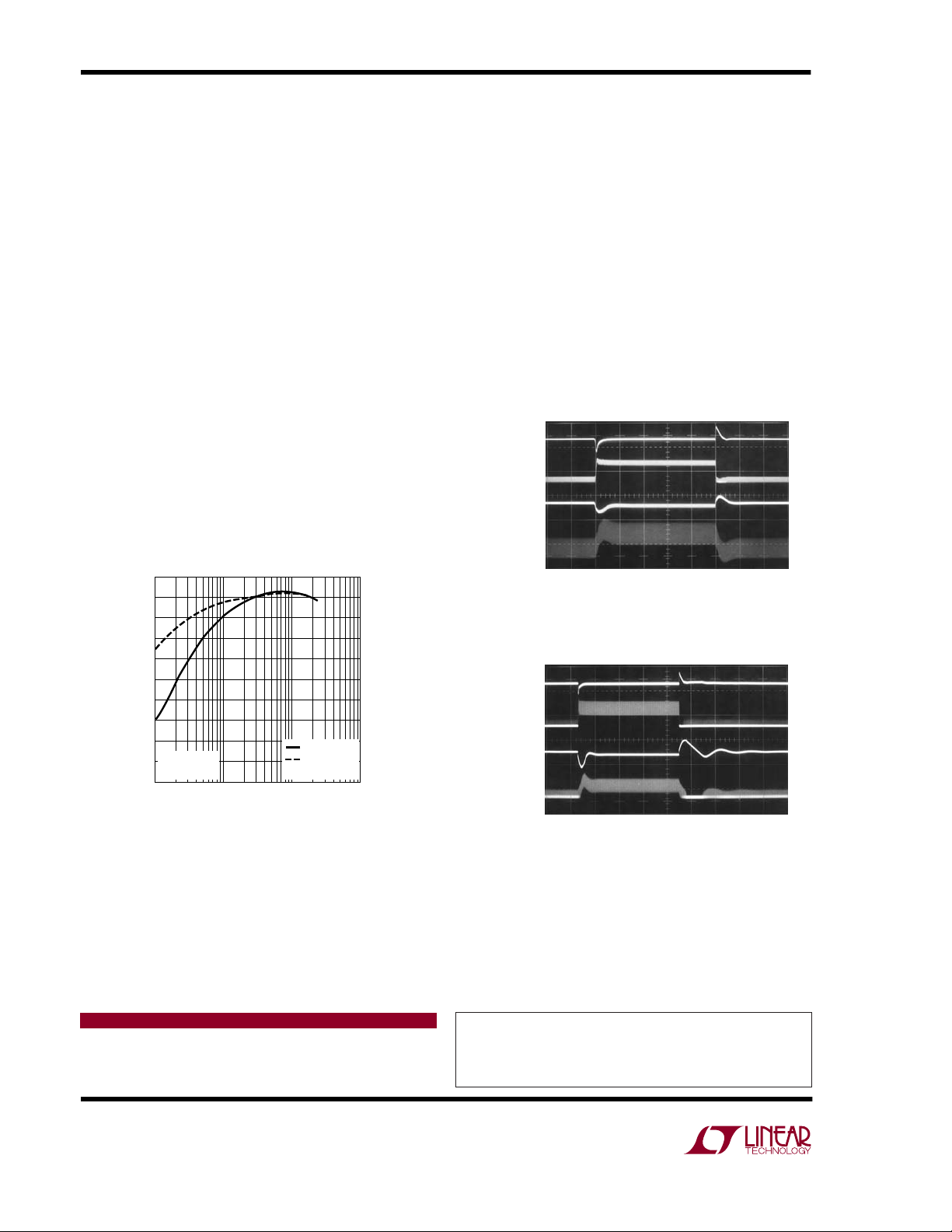
Figure 2 shows the efficiency of the core converter when
powered by a 2-cell alkaline. Efficiency reaches 93% at the
higher load currents. Burst Mode
®
operation improves
efficiency at light loads.
Figures 3 and 4 show the stable load step response of the
Core and Main outputs—±3% deviation from nominal—
for a 20mA to 150mA load transient on the Core output
and a 20mA to 100mA transient on the Main output.
Conclusion
With its low profile and seamless transition between input
power sources, the LTC3456 simplifies and shrinks power
supply designs for portable devices such as personal GPS
navigators, MP3 players, digital cameras and handheld
computers.
V
CORE
100mV/DIV
(AC COUPLED)
I
SW1
200mA/DIV
V
MAIN
200mV/DIV
(AC COUPLED)
I
SW2(BST)
200mA/DIV
100
90
80
70
60
50
40
EFFICIENCY (%)
30
20
V
10
= 2.4V
BATT
= 1.8V
V
CORE
0
1
10 100 1000
LOAD CURRENT (mA)
PWM MODE
Burst Mode
OPERATION
DN1006 F02
Figure 2. Core Converter Efficiency of the LTC3456
When Powered by a 2-Cell Alkaline
Data Sheet Download
http://www.linear.com
100µs/DIV
Figure 3. Load Transient (BATT = 2.4V)
V
CORE
100mV/DIV
(AC COUPLED)
I
SW1
200mA/DIV
V
MAIN
200mV/DIV
(AC COUPLED)
I
SW2
200mA/DIV
200µs/DIV
Figure 4. Load Transient (AC Wall/USB = 5V)
For applications help,
call (408) 432-1900, Ext. 2759
DN1006 F03
DN1006 F04
Linear Technology Corporation
1630 McCarthy Blvd., Milpitas, CA 95035-7417
(408) 432-1900 ● FAX: (408) 434-0507 ● www.linear.com
dn1006f 0905 • PRINTED IN THE USA
© LINEAR TECHNOLOGY CORPORATION 2005
 Loading...