

FEATURES
■
High Efficiency: Up to 96%
■
Very Low Quiescent Supply Current: 32µA During
Linear Regulator Operation
■
600mA Output Current (Buck Converter)
■
Optionally Operates as Linear Regulator Below
3mA—External or Automatic ON/OFF
■
2.5V to 5.5V Input Voltage Range
■
1.5MHz or 2.25MHz Constant Frequency Operation
or External Synchronization
■
No Schottky Diode Required
■
Low Dropout Operation: 100% Duty Cycle
■
0.6V Reference Allows Low Output Voltages
■
Shutdown Mode Draws <1µA Supply Current
■
Current Mode Operation for Excellent Line and
Load Transient Response
■
Overtemperature Protected
■
Low Profile (3mm × 3mm) 8-Lead DFN and 8-Lead
MSOP Packages
U
APPLICATIO S
■
Cellular Telephones
■
Personal Information Appliances
■
Wireless and DSL Modems
■
Digital Still Cameras
■
MP3 Players
■
Portable Instruments
, LTC and LT are registered trademarks of Linear Technology Corporation.
All other trademarks are the property of their respective owners.
Protected by U.S. Patents including 5481178, 6580258, 6304066, 6127815,
6498466, 6611131. Others pending.
LTC34 4 8
1.5MHz/2.25MHz, 600mA
Synchronous Step-Down
Regulator with LDO Mode
U
DESCRIPTIO
The LTC®3448 is a high efficiency, monolithic, synchronous
buck regulator using a constant frequency, current mode
architecture. Supply current during operation is only 32µA
(linear regulator mode) and drops to <1µA in shutdown. The
2.5V to 5.5V input voltage range makes the LTC3448 ideally suited for single Li-Ion battery-powered applications.
100% duty cycle provides low dropout operation, extending battery life in portable systems. At moderate output load
levels, PWM pulse skipping mode operation provides very
low output ripple voltage for noise sensitive applications.
The LTC3448 automatically switches into linear regulator
operation at very low load currents to maintain <5mV
output voltage ripple. Supply current in this mode is
typically 32µA. The switch to linear regulator mode occurs
at a threshold of 3mA. Linear regulator operation can be set
to on, off or automatic turn on/off.
Switching frequency is selectable at either 1.5MHz or
2.25MHz, allowing the use of small surface mount inductors and capacitors.
The internal synchronous switch increases efficiency and
eliminates the need for an external Schottky diode. Low
output voltages are easily supported with the 0.6V feedback reference voltage. The LTC3448 is available in a low
profile 3mm × 3mm DFN package or thermally enhanced
8-lead MSOP.
P-P
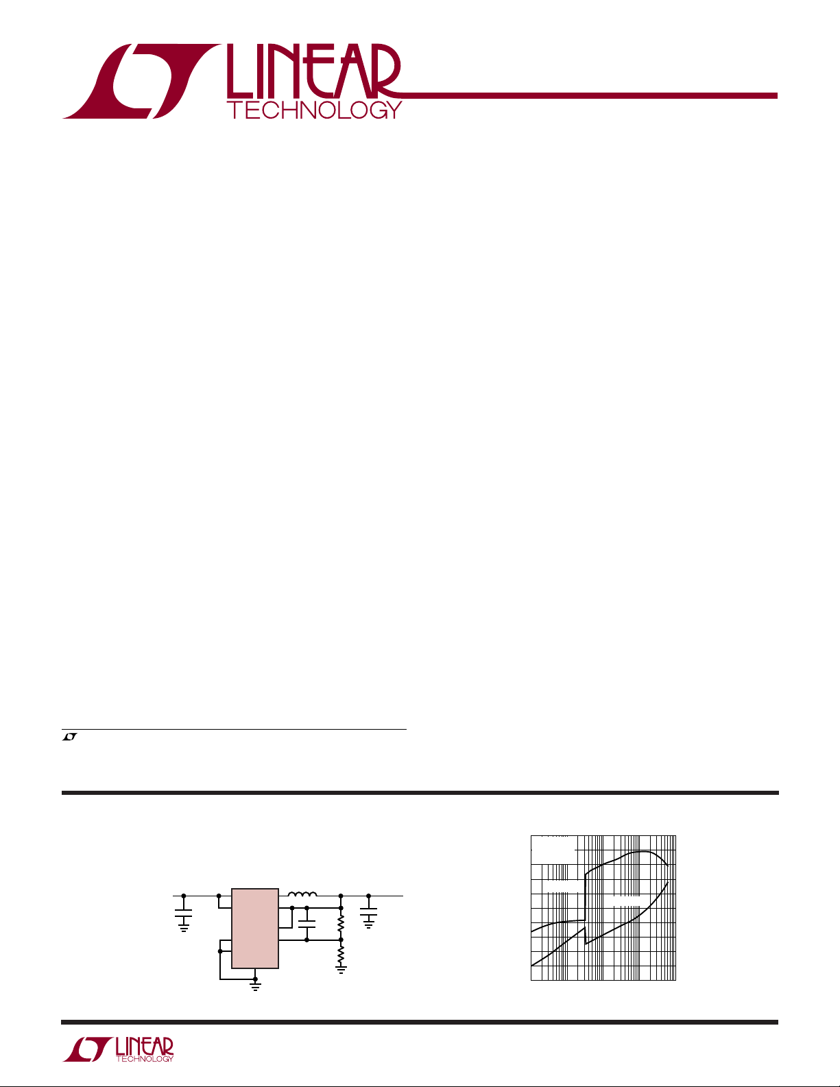
TYPICAL APPLICATIO
1.5V High Efficiency Regulator with Automatic LDO Mode
V
2.5V TO 5.5V
IN
C
IN
4.7µF
V
IN
RUN
LTC3448
FREQ
SYNC
GND
SW
V
OUT
MODE
V
3448 TA01a
U
2.2µH
474k
22pF
FB
316k
C
OUT
4.7µF
V
1.5V
OUT
Efficiency and Power Loss vs Load Current
100
VIN = 3.6V
= 1.5V
V
90
OUT
= 25°C
T
A
80
70
EFFICIENCY
60
50
40
EFFICIENCY (%)
30
20
10
0
0.0001 0.01 0.1 1
0.001
POWER LOSS
LOAD CURRENT (A)
23448 TA01b
1
0.1
POWER LOSS (W)
0.01
0.001
0.0001
3448f
1
LTC34 4 8
TOP VIEW
9
DD PACKAGE
8-LEAD (3mm × 3mm) PLASTIC DFN
5
6
7
8
4
3
2
1V
FB
V
OUT
MODE
V
IN
RUN
SYNC
FREQ
SW
WWWU
ABSOLUTE AXI U RATI GS
Input Supply Voltage .................................. – 0.3V to 6V
RUN, SYNC Voltages ................... –0.3V to (V
MODE Voltage ............................. – 0.3V to (V
FREQ, V
SW Voltage .................................. – 0.3V to (V
V
OUT
P-Channel Switch Source Current (DC) ............. 800mA
N-Channel Switch Sink Current (DC) ................. 800mA
Voltages...................... – 0.3V to (VIN + 0.3V)
FB
Voltage................................ – 0.3V to (VIN + 0.3V)
+ 0.3V)
IN
+ 0.3V)
IN
+ 0.3V)
IN
(Note 1)
V
(LDO) Source Current .................................. 25mA
OUT
Peak SW Sink and Source Current ........................ 1.3A
Operating Temperature Range (Note 2) .. –40°C to 85°C
Junction Temperature (Notes 3, 7) ...................... 125°C
Storage Temperature Range ................ –65°C to 125°C
Lead Temperature (Soldering, 10 sec)
MSOP Only ...................................................... 300°C
UU
W
PACKAGE/ORDER I FOR ATIO
ORDER PART
NUMBER
LTC3448EDD
V
OUT
MODE
DD PART MARKING
T
= 125°C, θJA = 43°C/ W
JMAX
EXPOSED PAD (PIN 9) IS GND
MUST BE SOLDERED TO PCB
Consult LTC Marketing for parts specified with wider operating temperature ranges.
ELECTRICAL CHARACTERISTICS
temperature range, otherwise specifications are TA = 25°C. VIN = 3.6V unless otherwise specified.
SYMBOL PARAMETER CONDITIONS MIN TYP MAX UNITS
I
VFB
V
FB
∆V
FB
∆V
OVL
∆V
OUT
I
PK
V
LOADREG
V
OUT(MAX)
V
IN
Feedback Current ● ±30 nA
Regulated Feedback Voltage TA = 25°C 0.5880 0.6 0.6120 V
(Note 4) 0°C ≤ T
Reference Voltage Line Regulation VIN = 2.5V to 5.5V (Note 4) ● 0.2 0.4 %/V
Output Overvoltage Lockout ∆V
Output Voltage Line Regulation VIN = 2.5V to 5.5V (LDO) 0.1 0.8 %/V
Peak Inductor Current VFB = 0.5V or V
Output Voltage Load Regulation LDO, 1mA to 10mA 0.5 %/V
Maximum Output Voltage (Note 9) VIN – 0.7 VIN – 0.3 V
Input Voltage Range ● 2.5 5.5 V
LBMJ
The ● denotes specifications which apply over the full operating
≤ 85°C 0.5865 0.6 0.6135 V
A
–40°C ≤ T
∆V
Duty Cycle < 35%
≤ 85°C ● 0.5850 0.6 0.6150 V
A
= V
= (V
– V
OVL
FB
– V
OVL
) • 100/V
OUT
= 90%, 0.7 1 1.3 A
OUT
OUT
OVL
OVL
TOP VIEW
V
1
FB
2
3
4
V
IN
MS8E PACKAGE
8-LEAD PLASTIC MSOP
T
= 125°C, θJA = 40°C/ W
JMAX
EXPOSED PAD (PIN 9) IS GND
MUST BE SOLDERED TO PCB
8
7
9
6
5
RUN
SYNC
FREQ
SW
15 35 55 mV
2.5 5.8 9.2 %
ORDER PART
NUMBER
LTC3448EMS8E
MS8 PART MARKING
LTBMK
2
3448f
LTC34 4 8
ELECTRICAL CHARACTERISTICS
The ● denotes specifications which apply over the full operating
temperature range, otherwise specifications are TA = 25°C. VIN = 3.6V unless otherwise specified.
SYMBOL PARAMETER CONDITIONS MIN TYP MAX UNITS
I
S
f
OSC
f
SYNC
V
TH(SYNC)
R
PFET
R
NFET
I
LSW
V
RUNH
V
RUNL
I
RUN
V
FREQH
V
FREQL
I
FREQ
V
MODEH
V
MODEL
I
MODE
I
SYNC
I
LDO(ON)
I
LDO(OFF)
Input DC Bias Current VIN = 3.6V (Note 5)
Active Mode (Pulse Skip, No LRO) V
Linear Regulator Operation (LRO) I
Shutdown V
= 0.5V or V
FB
= 0.5V or V
V
FB
≤ I
LOAD
LDO(ON)
= 0V, VIN = 5.5V 0.1 1 µA
RUN
= 90%, I
OUT
= 90%, I
OUT
= 0A, 1.5MHz 250 375 µA
LOAD
= 0A, 2.25MHz 275 400 µA
LOAD
32 43 µA
Oscillator Frequency FREQ = Low, VIN = 3.6V ● 1.2 1.5 1.8 MHz
FREQ = High
● 1.8 2.25 2.7 MHz
Synchronization Frequency (Note 6) 1.5 >4 MHz
SYNC Activation Input Threshold 1 1.3 V
R
of P-Channel FET ISW = 100mA 0.4 Ω
DS(ON)
R
of N-Channel FET ISW = –150mA 0.35 Ω
DS(ON)
SW Leakage V
= 0V, VSW = 0V or 5V, VIN = 5V ±0.01 ±1 µA
RUN
RUN Threshold High ● 1.5 V
RUN Threshold Low ● 0.3 V
RUN Leakage Current ● ±0.01 ±1 µA
FREQ Threshold High ● VIN – 1 V
FREQ Threshold Low ● 1V
FREQ Leakage Current ● ±0.01 ±1 µA
MODE Threshold High ● VIN – 0.15 V
MODE Threshold Low ● 0.12 V
MODE Leakage Current ● ±0.1 ±1 µA
SYNC Leakage Current ● ±0.01 ±1 µA
LRO ON Load Current Threshold 2.2mH Inductor (Note 8) 3 5 mA
LRO OFF Load Current Threhold 8 11 17 mA
Note 1: Absolute Maximum Ratings are those values beyond which the life
of a device may be impaired.
Note 2: The LTC3448E is guaranteed to meet performance specifications
from 0°C to 70°C. Specifications over the –40°C to 85°C operating
temperature range are assured by design, characterization and correlation
with statistical process controls.
Note 3: T
dissipation P
is calculated from the ambient temperature TA and power
J
according to the following formula:
D
T
= TA + (PD)(43°C/W)
J
Note 4: The LTC3448 is tested in a proprietary test mode that connects
to the output of the error amplifier.
V
FB
Note 5: Dynamic supply current is higher due to the gate charge being
delivered at the switching frequency. LRO is “linear regulator operation.”
Note 6: 4MHz operation is guaranteed by design but is not production
tested and is subject to duty cycle limitations.
Note 7: This IC includes overtemperature protection that is intended to
protect the device during momentary overload conditions. Junction
temperature will exceed 125°C when overtemperature is active. Continuous operation above the specified maximum operating junction temperature may impair device reliability.
Note 8: The load current below which the switching regulator turns off and
the LDO turns on is, to first order, inversely proportional to the value of
the inductor. This effect is covered in more detail in the Operation section.
This parameter is not production tested but is guaranteed by design.
Note 9: For 2.5V < V
< 2.7V the output voltage is limited to VIN – 0.7V
IN
to ensure regulation in linear regulator mode. This parameter is not
production tested but is guaranteed by design.
3448f
3
LTC34 4 8
LOAD CURRENT (A)
30
EFFICIENCY (%)
90
100
20
10
80
50
70
60
40
0.0001 0.01 0.1 1
23448 G03
0
0.001
V
OUT
= 1.5V
T
A
= 25°C
VIN = 2.7V
V
IN
= 3.6V
V
IN
= 4.2V
TEMPERATURE (°C)
–50
FREQUENCY (MHz)
1.65
25
3448 G06
1.50
1.40
–25 0 50
1.35
1.30
1.70
1.60
1.55
1.45
75 100 125
VIN = 3.6V
UW
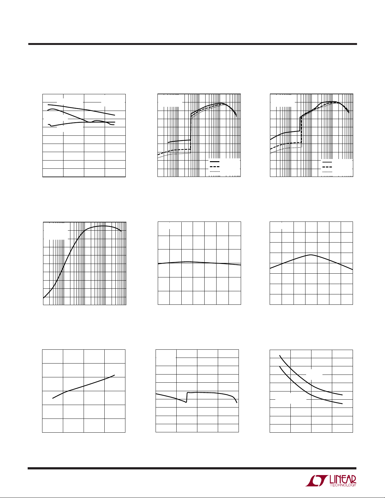
TYPICAL PERFOR A CE CHARACTERISTICS
(From Figure1a Except for the Resistive Divider Resistor Values)
Efficiency vs Input Voltage
100
95
90
I
= 30mA
OUT
85
80
75
70
EFFICIENCY (%)
65
60
55
50
2
I
= 100mA
OUT
I
= 600mA
OUT
3
INPUT VOLTAGE (V)
4
V
OUT
T
A
5
= 25°C
Efficiency vs Load Current
(Switcher Only)
100
VIN = 2.7V
90
= 2.5V
V
OUT
= 25°C
T
A
80
70
60
50
40
EFFICIENCY (%)
30
20
10
0
0.0001 0.01 0.1 1
0.001
LOAD CURRENT (A)
= 1.8V
3448 G01
23448 G04
6
0.615
0.610
0.605
0.600
0.595
REFERENCE VOLTAGE (V)
0.590
0.585
Efficiency vs Load Current
100
V
= 1.2V
OUT
90
= 25°C
T
A
80
70
60
50
40
EFFICIENCY (%)
30
20
10
0
0.0001 0.01 0.1 1
0.001
LOAD CURRENT (A)
VIN = 2.7V
= 3.6V
V
IN
= 4.2V
V
IN
23448 G02
Reference Voltage
vs Temperature
VIN = 3.6V
–50
–25 0
TEMPERATURE (°C)
50 100 125
25 75
3448 G05
Efficiency vs Load Current
Oscillator Frequency
vs Temperature
Oscillator Frequency
vs Supply Voltage
1.8
= 25°C
T
A
1.7
1.6
1.5
1.4
FREQUENCY (MHz)
1.3
1.2
4
2
34 56
SUPPLY VOLTAGE (V)
3448 G07
Output Voltage vs Load Current
1.525
VIN = 3.6V
1.520
= 25°C
T
A
1.515
1.510
1.505
1.500
1.495
1.490
OUTPUT VOLTAGE (V)
1.485
1.480
1.475
0.0001
0.001
0.01
LOAD CURRENT (A)
0.1
3448 G08
R
vs Input Voltage
DS(ON)
0.40
0.38
0.36
0.34
0.32
(Ω)
0.30
0.28
0.26
0.24
0.22
0.20
SYNCHRONOUS
2
DS(ON)
R
1
MAIN
SWITCH
SWITCH
3
4
INPUT VOLTAGE (V)
TA = 25°C
5
6
3448 G09
3448f

UW
TEMPERATURE (°C)
–50
DYNAMIC SUPPLY CURRENT (µA)
280
300
320
25 75
3448 G12
260
240
–25 0
50 100 125
220
200
VIN = 3.6V
I
LOAD
= 0A
2.25MHz
1.5MHz
TYPICAL PERFOR A CE CHARACTERISTICS
(From Figure1a Except for the Resistive Divider Resistor Values)
LTC34 4 8
R
vs Temperature
DS(ON)
0.6
0.5
0.4
(Ω)
0.3
DS(ON)
R
0.2
0.1
0
–50
MAIN SWITCH
–25 0
SYNCH SWITCH
2.5V
3.6V
4.2V
25 75
TEMPERATURE (°C)
2.5V
3.6V
4.2V
50 100 125
Switch Leakage vs Temperature
350
VIN = 5.5V
RUN = 0V
300
250
200
150
100
SWITCH LEAKAGE (nA)
50
0
–50
–25 0
SYNCHRONOUS
SWITCH
50 100 125
25 75
TEMPERATURE (°C)
MAIN
SWITCH
3448 G10
3448 G13
Dynamic Supply Current
vs Supply Voltage
340
I
= 0A
LOAD
= 25°C
T
A
320
300
280
260
240
DYNAMIC SUPPLY CURRENT (µA)
220
200
2
2.25MHz
1.5MHz
34
SUPPLY VOLTAGE (V)
Switch Leakage vs Input Voltage
10
RUN = 0V
= 25°C
T
A
1
0.1
SWITCH LEAKAGE (nA)
0.01
0.001
0
SYNCHRONOUS
1234
SWITCH
INPUT VOLTAGE (V)
SWITCH
5
MAIN
56
3448 G11
3448 G14
6
500mA/DIV
Dynamic Supply Current
vs Temperature
Start-Up from Shutdown
RUN
5V/DIV
V
OUT
1V/DIV
I
L
= 3.6V
V
IN
= 1.5V
V
OUT
= 600mA
I
LOAD
40µs/DIV
3448 G15
Load Step
V
OUT
200mV/DIV
AC COUPLED
I
LOAD
100mA/DIV
500mA/DIV
I
L
= 3.6V
V
IN
= 1.5V
V
OUT
I
LOAD
= 10µF
C
OUT
10µs/DIV
= 100µA TO 200mA
3448 G16
100mV/DIV
AC COUPLED
250mA/DIV
500mA/DIV
V
I
LOAD
OUT
I
Load Step
L
= 3.6V
V
IN
= 1.5V
V
OUT
= 50mA TO 600mA
I
LOAD
= 10µF
C
OUT
10µs/DIV
3448 G17
3448f
5
LTC34 4 8
UW
TYPICAL PERFOR A CE CHARACTERISTICS
(From Figure 1a Except for the Resistive Divider Resistor Values)
Load Step
V
V
OUT
100mV/DIV
AC COUPLED
I
LOAD
250mA/DIV
500mA/DIV
I
L
OUT
20mV/DIV
AC COUPLED
MODE PIN
2V/DIV
External Mode Control (Constant
1mA Load)
SWITCHER SWITCHER
LDO
3448 G18
U
V
= 3.6V
IN
= 1.5V
V
OUT
= 100mA TO 600mA
I
LOAD
10µs/DIV
UU
PI FU CTIO S
VFB (Pin 1): Feedback Pin. This pin receives the feedback
voltage from an external resistive divider across the
output.
V
(Pin 2): Output Pin. This pin connects to an external
OUT
resistor divider and the linear regulator output. Connect
externally to the inductor and the output capacitor. The
internal linear regulator will supply current up to the
I
LDO(OFF)
the buck regulator. Internal circuitry automatically enables
the buck switching regulator at load currents higher than
the I
pin is 2µF.
MODE (Pin 3): Linear Regulator Control. Grounding this
pin turns off the linear regulator. Setting this pin to V
turns on the linear regulator regardless of the load current.
Tying this pin midrange (i.e., to V
regulator in auto mode, where turn on/off is a function of
the load current. In applications where MODE is externally
driven high or low, this pin should be held low for 50µs
after the RUN pin is pulled high.
current. Load currents above that are supplied by
LDO(OFF)
. The minimum required capacitance on this
) will place the linear
OUT
IN
= 1.5V
V
OUT
= 25°C
T
A
V
(Pin 4): Main Supply Pin. This pin must be closely
IN
200µs/DIV
3448 G19
decoupled to GND with a 2.2µF or greater ceramic
capacitor.
SW (Pin 5): Switch Node Connection to Inductor. This pin
connects to the drains of the internal main and synchronous power MOSFET switches.
FREQ (Pin 6): Frequency Select. Switching frequency is
set to 1.5MHz when FREQ = 0V and to 2.25MHz when
FREQ = VIN. Do not float this pin.
SYNC (Pin 7): External Synchronization Pin. The oscillation frequency can be synchronized to an external oscillator applied to this pin. For external frequencies above
2.2MHz, pull FREQ high.
RUN (Pin 8): Run Control Input. Forcing this pin above
1.5V enables the part. Forcing this pin below 0.3V shuts
down the device. In shutdown, all functions are disabled
drawing <1µA supply current. Do not leave RUN floating.
Exposed Pad (Pin 9): Ground. This pin must be soldered
to PCB.
6
3448f

LTC34 4 8
U
U
W
FU CTIO AL DIAGRA
SYNC
7
FREQ
6
V
V
OUT
2
V
1
RUN
8
IN
LDO
DRIVE
FB
V
IN
0.6V REF
SHUTDOWN
OSC
0.6V
0.6V + ∆OVL
SLOPE
COMP
+
EA
–
–
OVDET
+
MODE
3
LDO CONTROL
LOGIC
V
4
3448 F01
IN
SW
5
GND
9
–
+
5Ω
OSC
Q
S
R
Q
RS LATCH
SWITCHING
LOGIC
AND
BLANKING
CIRCUIT
–
I
COMP
ANTI-
SHOOT-
THRU
I
RCMP
+
+
–
Figure 1
U
OPERATIO
Main Control Loop
The LTC3448 uses a constant frequency, current mode,
step-down architecture. Both the main (P-channel MOSFET) and synchronous (N-channel MOSFET) switches are
internal. During normal operation, the internal top power
MOSFET is turned on each cycle when the oscillator sets
the RS latch, and turned off when the current comparator,
I
, resets the RS latch. The peak inductor current at
COMP
which I
output of error amplifier EA. When the load current
increases, it causes a slight decrease in the feedback
voltage FB
causes the EA amplifier’s output voltage to increase until
the average inductor current matches the new load current. While the top MOSFET is off, the bottom MOSFET is
turned on until either the inductor current starts to reverse, as indicated by the current reversal comparator
I
, or the beginning of the next clock cycle. The
RCMP
resets the RS latch, is controlled by the
COMP
relative to the 0.6V reference, which in turn,
INT
(Refer to Functional Diagram)
comparator OVDET guards against transient overshoots
5.8% by turning off the main switch and keeping it off until
the fault is removed.
Pulse Skipping Mode Operation
At light loads, the inductor current may reach zero or
reverse on each pulse. The bottom MOSFET is turned off
by the current reversal comparator, I
, and the switch
RCMP
voltage will ring. This is discontinuous mode operation,
and is normal behavior for the switching regulator. At very
light loads, the LTC3448 will automatically skip pulses to
maintain output regulation.
Low Ripple LDO Mode Operation
At load currents below I
LDO(ON),
and when enabled, the
LTC3448 will switch into very low ripple, linear regulating
operation (LRO). In this mode, the current is sourced from
3448f
7

LTC34 4 8
OPERATIO
U
(Refer to Functional Diagram)
the V
pin and both the main and synchronous switches
OUT
are turned off. The control loop is stabilized by the load
capacitor and requires a minimum value of 2µF. The
LTC3448 will change back to switching mode and turn off
the LDO when the load current exceeds approximately
11mA.
When MODE is connected to an intermediate voltage level
(i.e., V
), this switchover is automatic. If MODE is pulled
OUT
high to VIN, the LDO remains on and the switcher off
regardless of the load current. The LDO is capable of
providing a maximum of approximately 15mA before the
load regulation will degrade to unacceptable levels. If
MODE is pulled to GND, the switcher remains on and the
LDO off regardless of the load current.
4.5
4.0
3.5
3.0
(mA)
2.5
2.0
LDO(ON)
I
1.5
1.0
0.5
5.0
4.5
4.0
3.5
3.0
(mA)
2.5
2.0
LDO(ON)
I
1.5
1.0
0.5
0
0
2
Figure 2. I
2
0
Figure 3. I
V
= 1.2V
OUT
V
= 1.5V
OUT
V
= 1.8V
OUT
VIN (V)
LDO(ON)
4
4
68
LDO(ON)
3
INDUCTOR VALUE (µH)
TA = 25°C
L = 2.2µH
5
vs VIN, V
VIN = 3.6V
V
OUT
= 25°C
T
A
vs L
OUT
3448 F02
OUT
= 1.5V
10
3448 F03
6
12
Some applications may be able to anticipate the transition
from high to low and low to high load currents. In these
cases it may be desirable to switch between modes by
controlling the MODE pin with a processor signal. In these
applications it is important that the MODE pin is pulled
high no earlier than 50µs after the RUN pin is pulled high.
This will ensure proper start-up of internal reference
circuitry.
The load current I
LDO(ON)
below which the switcher will
automatically turn off and the LDO turn on is independent
of the external capacitor, and to first order, independent
of supply and output voltage. There is an inverse relationship between I
LDO(ON)
and the value of the inductor.
These dependencies are shown in Figures 2 and 3.
Automatic operation with inductor values below 1µH is
not recommended.
At the low load currents at which the switcher to linear
regulator transition occurs, the switcher is operating in
pulse skipping mode. During each switching cycle in this
mode, while the synchronous switch (bottom MOSFET) is
on, the inductor current decays until the reverse current
comparator is triggered. At this occurrence, the bottom
MOSFET is turned off. Ideally, this occurs when the
inductor current is precisely zero. In reality, because of onchip delays, this current will be negative at higher output
voltages.
The internal algorithm which controls the LDO turn-on
load current level makes certain assumptions about the
amount of charge transferred to the output on each
switching cycle. These assumptions are no longer met
when the inductor current begins to reverse. This causes
the load current at which the transition takes place to move
to lower levels at higher output voltages. For this reason
use of the LDO auto mode is not recommended for output
levels above 2V. For output voltages above 2V, the MODE
pin should be driven externally.
Short-Circuit Protection
When the output is shorted to ground, the main switch
cycle will be skipped, and the synchronous switch will
remain on for a longer duration. This allows the inductor
current more time to decay, thereby preventing runaway.
8
3448f

OPERATIO
LTC34 4 8
U
(Refer to Functional Diagram)
1200
1000
V
= 1.8V
OUT
800
V
= 1.5V
OUT
600
400
200
MAXIMUM OUTPUT CURRENT (mA)
0
2.5
3.0
Figure 4. Maximum Output Current vs Input Voltage
V
= 2.5V
OUT
3.5 4.0 4.5
SUPPLY VOLTAGE (V)
5.0 5.5
3448 F04
Dropout Operation
As the input supply voltage decreases to a value approaching the output voltage, the duty cycle increases toward the
maximum on-time. Further reduction of the supply voltage
forces the main switch to remain on for more than one cycle
until it reaches 100% duty cycle. The output voltage will then
be determined by the input voltage minus the voltage drop
across the P-channel MOSFET and the inductor.
An important detail to remember is that at low input supply
voltages, the R
of the P-channel switch increases
DS(ON)
(see Typical Performance Characteristics). Therefore, the
user should calculate the power dissipation when the
LTC3448 is used at 100% duty cycle with low input voltage
(See Thermal Considerations in the Applications Information section).
Low Supply Operation
The LTC3448 will operate with input supply voltages as
low as 2.5V, but the maximum allowable output current is
reduced at this low voltage. Figure 4 shows the reduction
in the maximum output current as a function of input
voltage for various output voltages.
Slope Compensation and Inductor Peak Current
Slope compensation provides stability in constant frequency architectures by preventing sub-harmonic oscillations at high duty cycles. It is accomplished internally by
adding a compensating ramp to the inductor current
signal at duty cycles in excess of 40%. This normally
results in a reduction of maximum inductor peak current
for duty cycles >40%. However, the LTC3448 uses a
patent-pending scheme that counteracts this compensat-
ing ramp, which allows the maximum inductor peak
current to remain unaffected throughout all duty cycles.
WUUU
APPLICATIO S I FOR ATIO
The basic LTC3448 application circuit is shown on the first
page of this data sheet. External component selection is
driven by the load requirement and begins with the selection of L followed by C
Inductor Selection
For most applications, the value of the inductor will fall in
the range of 1µH to 4.7µH. Its value is chosen based on the
desired ripple current. Large value inductors lower ripple
current and small value inductors result in higher ripple
currents. Higher VIN or V
current as shown in equation 1. A reasonable starting point
for setting ripple current is ∆IL = 240mA (40% of 600mA).
IN
and C
OUT
.
OUT
also increases the ripple
∆ =
I
1
L OUT
fL
()( )
⎛
1
V
−
⎜
⎝
V
OUT
V
IN
⎞
⎟
⎠
(1)
The DC current rating of the inductor should be at least
equal to the maximum load current plus half the ripple
current to prevent core saturation. Thus, a 720mA rated
inductor should be enough for most applications (600mA
+ 120mA). For better efficiency, choose a low DC-resistance inductor.
If the LTC3448 is to be used in auto LDO mode, inductor
values less than 1µH should not be used.
3448f
9

LTC34 4 8
WUUU
APPLICATIO S I FOR ATIO
Inductor Core Selection
Different core materials and shapes will change the size/
current and price/current relationship of an inductor.
Toroid or shielded pot cores in ferrite or permalloy materials are small and don’t radiate much energy, but generally cost more than powdered iron core inductors with
similar electrical characteristics. The choice of which style
inductor to use often depends more on the price vs size
requirements and any radiated field/EMI requirements
than on what the LTC3448 requires to operate. Table 1
shows some typical surface mount inductors that work
well in LTC3448 applications.
Table 1. Representative Surface Mount Inductors
PART VALUE DCR MAX DC SIZE
NUMBER (µH) (Ω MAX) CURRENT (A) W × L × H (mm
Sumida 1.5 0.043 1.55 3.8 × 3.8 × 1.8
CDRH3D16 2.2 0.075 1.20
3.3 0.110 1.10
4.7 0.162 0.90
Sumida 2.2 0.116 0.950 3.5 × 4.3 × 0.8
CMD4D06 3.3 0.174 0.770
4.7 0.216 0.750
Coilcraft 2.2 0.104 1.8 2.5 × 3.2 × 2.0
ME3220 3.3 0.138 1.3
4.7 0.190 1.2
Murata 1.0 0.060 1.00 2.5 × 3.2 × 2.0
LQH3C 2.2 0.097 0.79
4.7 0.150 0.65
CIN and C
Selection
OUT
3
)
In continuous mode, the source current of the top MOSFET is a square wave of duty cycle V
OUT/VIN
. To prevent
large voltage transients, a low ESR input capacitor sized
for the maximum RMS current must be used. The maximum RMS capacitor current is given by:
12/
VVV
OUT IN OUT
CI
required I
IN OMAX
RMS
≅
[]
This formula has a maximum at VIN = 2V
I
RMS
= I
/2. This simple worst-case condition is com-
OUT
−
()
V
IN
, where
OUT
monly used for design. Note that the capacitor
manufacturer’s ripple current ratings are often based on
2000 hours of life. This makes it advisable to further derate
the capacitor, or choose a capacitor rated at a higher
temperature than required. Always consult the manufacturer if there is any question.
The selection of C
is driven by the required effective
OUT
series resistance (ESR). Typically, once the ESR requirement for C
generally far exceeds the I
case, if LDO mode is enabled, the value of C
has been met, the RMS current rating
OUT
RIPPLE(P-P)
requirement. In any
must have
OUT
a minimum value of 2µF to ensure loop stability. The
output ripple ∆V
∆≅∆ +
V I ESR
OUT L
where f = operating frequency, C
is determined by:
OUT
⎛
⎜
⎝
1
8
fC
OUT
⎞
⎟
⎠
= output capacitance
OUT
and ∆IL = ripple current in the inductor. For a fixed output
voltage, the output ripple is highest at maximum input
voltage since ∆IL increases with input voltage.
Aluminum electrolytic and dry tantalum capacitors are
both available in surface mount configurations. In the case
of tantalum, it is critical that the capacitors are surge tested
for use in switching power supplies. An excellent choice is
the AVX TPS series of surface mount tantalum. These are
specially constructed and tested for low ESR so they give
the lowest ESR for a given volume. Other capacitor types
include Sanyo POSCAP, Kemet T510 and T495 series, and
Sprague 593D and 595D series. Consult the manufacturer
for other specific recommendations.
Using Ceramic Input and Output Capacitors
Higher values, lower cost ceramic capacitors are now
becoming available in smaller case sizes. Their high ripple
current, high voltage rating and low ESR make them ideal
for switching regulator applications. Because the
LTC3448’s control loop does not depend on the output
capacitor’s ESR for stable operation, ceramic capacitors
can be used freely to achieve very low output ripple and
small circuit size.
However, care must be taken when ceramic capacitors are
used at the input and the output. When a ceramic capacitor
is used at the input and the power is supplied by a wall
adapter through long wires, a load step at the output can
induce ringing at the input, VIN. At best, this ringing can
couple to the output and be mistaken as loop instability. At
3448f
10

WUUU
APPLICATIO S I FOR ATIO
LTC34 4 8
worst, a sudden inrush of current through the long wires
can potentially cause a voltage spike at VIN, large enough
to damage the part.
When choosing the input and output ceramic capacitors,
choose the X5R or X7R dielectric formulations. These
dielectrics have the best temperature and voltage characteristics of all the ceramics for a given value and size.
Output Voltage Programming
The output voltage is set by tying VFB to a resistive divider
according to the following formula:
VV
⎛
=+
06 1
OUT
.
⎜
⎝
⎞
R
2
⎟
R
1
⎠
(2)
The external resistive divider is connected to the output,
allowing remote voltage sensing as shown in Figure 5.
0.6V ≤ V
V
FB
LTC3448
GND
Figure 5. Setting the LTC3448 Output Voltage
OUT
≤ 5.5V
R2
R1
3448 F05
Efficiency Considerations
The efficiency of a switching regulator is equal to the
output power divided by the input power times 100%. It is
often useful to analyze individual losses to determine what
is limiting the efficiency and which change would produce
the most improvement. Efficiency can be expressed as:
Efficiency = 100% – (L1 + L2 + L3 + ...)
where L1, L2, etc. are the individual losses as a percentage
of input power.
Although all dissipative elements in the circuit produce
losses, two main sources usually account for most of the
losses in LTC3448 circuits: VIN quiescent current and I2R
losses. When in switching mode, VIN quiescent current
loss dominates the efficiency loss at low load currents,
whereas the I2R loss dominates the efficiency loss at
medium to high load currents. At very low load currents
with the part operating in LDO mode, efficiency can be
dominated by I2R losses in the pass transistor and is a
strong function of (VIN – V
). In a typical efficiency plot,
OUT
the efficiency curve at very low load currents can be
misleading since the actual power lost is of little consequence as illustrated in Figure 6.
1
VIN = 3.6V
FREQ = 0V
LDOCNTRL = V
0.1
0.01
POWER LOSS (W)
0.001
0.0001
0.0001
Figure 6. Power Loss vs Load Current
OUT(AUTO)
0.010.001 10.1
LOAD CURRENT (A)
1.2V
1.5V
1.8V
3448 F06
1. The VIN quiescent current is due to two components:
the DC bias current as given in the Electrical Characteristics and the internal main switch and synchronous
switch gate charge currents. The gate charge current
results from switching the gate capacitance of the
internal power MOSFET switches. Each time the gate is
switched from high to low to high again, a packet of
charge, dQ, moves from VIN to ground. The resulting
dQ/dt is the current out of VIN that is typically larger than
the DC bias current and proportional to frequency. Both
the DC bias and gate charge losses are proportional to
VIN and thus their effects will be more pronounced at
higher supply voltages.
2. I2R losses are calculated from the resistances of the
internal switches, RSW, and external inductor RL. In
continuous mode, the average output current flowing
through inductor L is “chopped” between the main
switch and the synchronous switch. Thus, the series
resistance looking into the SW pin is a function of both
3448f
11

LTC34 4 8
WUUU
APPLICATIO S I FOR ATIO
top and bottom MOSFET R
and the duty cycle
DS(ON)
(DC) as follows:
RSW = (R
The R
DS(ON)
DS(ON)TOP
for both the top and bottom MOSFETs can
)(DC) + (R
DS(ON)BOT
)(1 – DC)
be obtained from the Typical Performance Characteristics curves. Thus, to obtain I2R losses, simply add R
SW
to RL and multiply the result by the square of the
average output current.
3. At load currents below the selected threshold the
LTC3448 will switch into low ripple LDO mode if enabled. In this case the losses are due to the DC bias
currents as given in the electrical characteristics and
I2R losses due to the (VIN – V
) voltage drop across
OUT
the internal pass transistor.
Other losses when in switching operation, including C
IN
and COUT ESR dissipative losses and inductor core losses,
generally account for less than 2% total additional loss.
Thermal Considerations
The LTC3448 requires the package backplane metal (GND
pin) to be well soldered to the PC board. This gives the DFN
and MSOP packages exceptional thermal properties, making it difficult in normal operation to exceed the maximum
junction temperature of the part. In most applications the
LTC3448 does not dissipate much heat due to its high
efficiency. In applications where the LTC3448 is running at
high ambient temperature with low supply voltage and high
duty cycles, such as in dropout, the heat dissipated may
exceed the maximum junction temperature of the part if it
is not well thermally grounded. If the junction temperature
reaches approximately 150°C, both power switches will be
turned off and the SW node will become high impedance.
To avoid the LTC3448 from exceeding the maximum
junction temperature, the user will need to do some
thermal analysis. The goal of the thermal analysis is to
determine whether the power dissipated exceeds the
maximum junction temperature of the part. The temperature rise is given by:
TR = PDθ
JA
where PD is the power dissipated by the regulator and θ
JA
is the thermal resistance from the junction of the die to the
ambient temperature.
The junction temperature, TJ, is given by:
TJ = TA + T
R
where TA is the ambient temperature.
As an example, consider the LTC3448 in dropout at an
input voltage of 2.7V, a load current of 600mA and an
ambient temperature of 70°C. From the typical performance graph of switch resistance, the R
DS(ON)
of the
P-channel switch at 70°C is approximately 0.52Ω. Therefore, power dissipated by the part is:
LOAD
2
• R
DS(ON)
= 187.2mW
PD = I
For the 3mm × 3mm DFN package, the θJA is 43°C/W.
Thus, the junction temperature of the regulator is:
TJ = 85°C + (0.1872)(43) = 93°C
which is well below the maximum junction temperature of
125°C.
Note that at higher supply voltages, the junction temperature is lower due to reduced switch resistance R
DS(ON).
Checking Transient Response
The regulator loop response can be checked by looking at
the load transient response. Switching regulators take
several cycles to respond to a step in load current. When
a load step occurs, V
equal to (∆I
resistance of C
charge C
OUT
• ESR), where ESR is the effective series
LOAD
OUT
, which generates a feedback error signal. The
regulator loop then acts to return V
value. During this recovery time V
immediately shifts by an amount
OUT
. ∆I
also begins to charge or dis-
LOAD
to its steady-state
OUT
can be monitored for
OUT
overshoot or ringing that would indicate a stability problem. For a detailed explanation of switching control loop
theory, see Application Note 76.
A second, more severe transient is caused by switching in
loads with large (>1µF) supply bypass capacitors. The
discharged bypass capacitors are effectively put in parallel
12
3448f

WUUU
APPLICATIO S I FOR ATIO
LTC34 4 8
with C
, causing a rapid drop in V
OUT
. No regulator can
OUT
deliver enough current to prevent this problem if the load
switch resistance is low and it is driven quickly. The only
solution is to limit the rise time of the switch drive so that
the load rise time is limited to approximately (25 • C
LOAD
).
Thus, a 10µF capacitor charging to 3.3V would require a
250µs rise time, limiting the charging current to about
130mA.
PC Board Layout Checklist
When laying out the printed circuit board, the following
checklist should be used to ensure proper operation of the
LTC3448. These items are also illustrated graphically in
Figures 7 and 8. Check the following in your layout:
1. The power traces, consisting of the GND trace, the SW
trace and the VIN trace should be kept short, direct and
wide.
GND
SW
V
OUT
MODE
V
9
5
2
3
1
FB
V
IN
4
V
IN
8
RUN
C
IN
LTC3448
6
FREQ
7
SYNC
2. Does the VFB pin connect directly to the feedback
resistors? The resistive divider R1/R2 must be connected between the (+) plate of C
and ground.
OUT
3. Does the (+) plate of CIN connect to VIN as closely as
possible? This capacitor provides the AC current to the
internal power MOSFETs.
4. Keep the switching node, SW, away from the sensitive
VFB node.
5. Keep the (–) plates of CIN and C
as close as possible.
OUT
Design Example
As a design example, assume the LTC3448 is used in a
single lithium-ion battery-powered cellular phone
application. The VIN will be operating from a maximum of
4.2V down to about 2.7V. The load current requirement
is a maximum of 0.6A but most of the time it will be in
standby mode, requiring only 2mA. Efficiency at both low
L
R
FB2
R
FB1
3448 F07
C
FF
V
OUT
C
OUT
Figure 7. LTC3448 Layout Design
Figure 8. LTC3448 Layout
3448 F08
3448f
13

LTC34 4 8
WUUU
APPLICATIO S I FOR ATIO
and high load currents is important. Output voltage is
1.8V. With this information we can calculate L using
Equation (1),
L
1
=
fI
L
()∆()
Substituting V
V
OUT
OUT
⎛
−
1
⎜
⎝
= 1.8V, V
⎞
V
OUT
⎟
V
⎠
IN
= 4.2V, ∆IL = 240mA and
IN
(3)
f = 1.5MHz in Equation (3) gives:
V
18
L
1 5 240
.
MHz mA
.( )..
⎛
1
⎜
⎝
18
42
V
⎞
=µ
286
.
⎟
⎠
V
H= −
A 2.2µH inductor works well for this application. For best
efficiency choose a 720mA or greater inductor with less
than 0.2Ω series resistance.
V
2.7V
TO 5.5V
IN
4
V
IN
8
C
IN
4.7µF
CER
RUN
LTC3448
6
FREQ
7
SYNC
GND
C
: TAIYO YUDEN JMK212BJ475MG
IN
: TAIYO YUDEN JMK212BJ475MG
C
OUT
*MURATA LQH32CN2R2M11
MODE
9
2.2µH*
5
SW
2
V
OUT
3
1
V
FB
3448 F09a
Figure 9a
22pF
632k
316k
C
OUT
15µF
CER
V
OUT
1.8V
C
will require an RMS current rating of at least 0.3A ≅
IN
I
LOAD(MAX)
/2 at temperature and C
will require an ESR
OUT
of less than 0.25Ω. In most cases, a ceramic capacitor will
satisfy this requirement.
For the feedback resistors, choose R1 = 316k. R2 can
then be calculated from Equation (2) to be:
V
⎛
R
2
OUT
⎜
⎝
06
⎞
Rk
1 1 632= −
=
⎟
⎠
.
Figure 9 shows the complete circuit along with its efficiency curve.
100
VIN = 3.6V
90
= 1.8V
V
OUT
= 25°C
T
A
80
70
60
50
40
EFFICIENCY (%)
30
20
10
0
0.0001 0.01 0.1 1
0.001
LOAD CURRENT (A)
3448 F09b
Figure 9b
100mV/DIV
AC COUPLED
I
100mA/DIV
500mA/DIV
14
V
OUT
LOAD
I
L
V
= 3.6V
IN
V
OUT
I
LOAD
= 1.8V
= 100µA TO 200mA
20µs/DIV
Figure 9c
3448 F09c
V
OUT
100mV/DIV
AC COUPLED
I
LOAD
250mA/DIV
500mA/DIV
I
L
V
= 3.6V
IN
V
OUT
I
LOAD
= 1.8V
= 50mA TO 600mA
20µs/DIV
Figure 9d
3448 F09d
3448f

TYPICAL APPLICATIO S
LTC34 4 8
U
V
IN
2.7V
TO 5.5V
V
OUT
100mV/DIV
AC COUPLED
I
LOAD
100mA/DIV
Single Li-Ion 1.5V/600mA Regulator for
High Efficiency and Small Footprint
2.2µH*
MODE
GND
V
9
3448 TA03
SW
OUT
V
FB
5
2
3 22pF
1
474k
216k
4
V
IN
8
C
IN
4.7µF
CER
RUN
LTC3448
6
FREQ
7
SYNC
C
: TAIYO YUDEN CERAMIC JMK212BJ475MG
IN
: TAIYO YUDEN CERAMIC JMK212BJ475MG
C
OUT
*MURATA LQH32CN2R2M33
C
OUT
15µF
V
OUT
1.5V
V
OUT
100mV/DIV
AC COUPLED
I
LOAD
250mA/DIV
Efficiency vs Output Current
100
V
= 1.5V
OUT
90
= 25°C
T
A
80
70
60
50
40
EFFICIENCY (%)
30
20
10
0
0.0001 0.01 0.1 1
0.001
LOAD CURRENT (A)
VIN = 2.7V
= 3.6V
V
IN
= 4.2V
V
IN
Load StepLoad Step
23448 G03
I
L
500mA/DIV
V
= 3.6V
IN
= 1.5V
V
OUT
= 100µA TO 200mA
I
LOAD
20µs/DIV
3448 TA05
Note: Performance data measured on the LTC3448 with external resistors
500mA/DIV
I
L
V
= 3.6V
IN
V
OUT
I
LOAD
= 1.5V
= 50mA TO 600mA
20µs/DIV
3448 TA06
3448f
15

LTC34 4 8
TYPICAL APPLICATIO S
Single Li-Ion 1.2V/600mA Regulator for
High Efficiency and Small Footprint Efficiency vs Output Current
U
V
IN
2.7V
TO 5.5V
V
100mV/DIV
AC COUPLED
I
LOAD
100mA/DIV
OUT
4
V
IN
8
C
IN
4.7µF
CER
RUN
LTC3448
6
FREQ
7
SYNC
GND
C
: TAIYO YUDEN JMK212BJ475MG
IN
: TAIYO YUDEN JMK212BJ475MG
C
OUT
*MURATA LQH32CN2R2M33
SW
V
OUT
MODE
V
9
3448 TA07
2.2µH*
5
2
3
1
FB
22pF
316k
316k
C
OUT
10µF
CER
V
OUT
1.2V
100
V
= 1.2V
OUT
90
T
= 25°C
A
80
70
60
50
40
EFFICIENCY (%)
30
20
10
0
0.0001 0.01 0.1 1
0.001
LOAD CURRENT (A)
VIN = 2.7V
= 3.6V
V
IN
= 4.2V
V
IN
23448 G02
Load StepLoad Step
V
OUT
100mV/DIV
AC COUPLED
I
LOAD
250mA/DIV
500mA/DIV
I
L
V
= 3.6V
IN
V
OUT
I
LOAD
= 1.2V
= 100µA TO 200mA
20µs/DIV
3448 TA09
500mA/DIV
I
L
= 3.6V
V
IN
V
OUT
I
LOAD
= 1.2V
= 50mA TO 600mA
20µs/DIV
3448 TA10
3448f
16

TYPICAL APPLICATIO S
Single Li-Ion 2.5V/600mA Regulator with 1.8MHz External
LTC34 4 8
U
Synchronization and External MODE
V
OUT
100mV/DIV
AC COUPLED
LDOCNTRL
2V/DIV
I
LOAD
250mA/DIV
= 3.6V
V
IN
= 2.5V
V
OUT
= 100µA TO 300mA
I
LOAD
V
2.5V TO 5.5V
OR GREATER 1.8MHz
EXTERNAL CLOCK
IN
µPROCESSOR
CONTROL
TO 0V TO 1.3V
C
IN
4.7µF
CER
2.2µH
GND
V
9
3448 TA12
SW
OUT
V
5
2
C
1.58M
1
FB
500k
FF
22pF
4
V
IN
8
RUN
LTC3448
TO
3
MODE
6
FREQ
7
SYNC
C
OUT
10µF
CER
V
OUT
2.5V
600mA
Load Step Load Step
V
OUT
100mV/DIV
AC COUPLED
LDOCNTRL
2V/DIV
I
LOAD
250mA/DIV
40µs/DIV
3448 TA12b
= 3.6V
V
IN
= 2.5V
V
OUT
= 100µA TO 600mA
I
LOAD
40µs/DIV
3448 TA12c
Single Li-Ion 1.2V/600mA Regulator with 2.5MHz External Synchronization
V
2.5V TO 5.5V
TO 0V TO 1.3V OR
GREATER 2.5MHz
EXTERNAL CLOCK
2.2µH
GND
SW
V
OUT
MODE
V
9
3448 TA13
5
2
C
316k
3
1
FB
316k
FF
22pF
IN
C
IN
4.7µF
CER
4
8
6
7
V
IN
RUN
LTC3448
FREQ
SYNC
C
OUT
10µF
CER
V
OUT
1.2V
600mA
3448f
17

LTC34 4 8
PACKAGE DESCRIPTIO
U
DD Package
8-Lead Plastic DFN (3mm × 3mm)
(Reference LTC DWG # 05-08-1698)
0.675 ±0.05
3.5 ±0.05
1.65 ±0.05
(2 SIDES)2.15 ±0.05
PACKAGE
OUTLINE
0.25 ± 0.05
RECOMMENDED SOLDER PAD PITCH AND DIMENSIONS
PIN 1
TOP MARK
(NOTE 6)
0.200 REF
NOTE:
1. DRAWING TO BE MADE A JEDEC PACKAGE OUTLINE M0-229 VARIATION OF (WEED-1)
2. DRAWING NOT TO SCALE
3. ALL DIMENSIONS ARE IN MILLIMETERS
4. DIMENSIONS OF EXPOSED PAD ON BOTTOM OF PACKAGE DO NOT INCLUDE
MOLD FLASH. MOLD FLASH, IF PRESENT, SHALL NOT EXCEED 0.15mm ON ANY SIDE
5. EXPOSED PAD SHALL BE SOLDER PLATED
6. SHADED AREA IS ONLY A REFERENCE FOR PIN 1 LOCATION
ON TOP AND BOTTOM OF PACKAGE
0.50
BSC
2.38 ±0.05
(2 SIDES)
3.00 ±0.10
(4 SIDES)
0.75 ±0.05
0.00 – 0.05
1.65 ± 0.10
(2 SIDES)
R = 0.115
TYP
0.25 ± 0.05
2.38 ±0.10
(2 SIDES)
BOTTOM VIEW—EXPOSED PAD
0.38 ± 0.10
85
14
0.50 BSC
(DD8) DFN 1203
18
3448f

PACKAGE DESCRIPTIO
2.794 ± 0.102
(.110 ± .004)
U
MS8E Package
8-Lead Plastic MSOP
(Reference LTC DWG # 05-08-1662)
0.889 ± 0.127
(.035 ± .005)
BOTTOM VIEW OF
EXPOSED PAD OPTION
1
LTC34 4 8
2.06 ± 0.102
(.081 ± .004)
1.83 ± 0.102
(.072 ± .004)
5.23
(.206)
MIN
0.42 ± 0.038
(.0165 ± .0015)
TYP
RECOMMENDED SOLDER PAD LAYOUT
0.254
(.010)
GAUGE PLANE
0.18
(.007)
NOTE:
1. DIMENSIONS IN MILLIMETER/(INCH)
2. DRAWING NOT TO SCALE
3. DIMENSION DOES NOT INCLUDE MOLD FLASH, PROTRUSIONS OR GATE BURRS.
MOLD FLASH, PROTRUSIONS OR GATE BURRS SHALL NOT EXCEED 0.152mm (.006") PER SIDE
4. DIMENSION DOES NOT INCLUDE INTERLEAD FLASH OR PROTRUSIONS.
INTERLEAD FLASH OR PROTRUSIONS SHALL NOT EXCEED 0.152mm (.006") PER SIDE
5. LEAD COPLANARITY (BOTTOM OF LEADS AFTER FORMING) SHALL BE 0.102mm (.004") MAX
DETAIL “A”
DETAIL “A”
2.083 ± 0.102
(.082 ± .004)
0.65
(.0256)
BSC
0° – 6° TYP
3.20 – 3.45
(.126 – .136)
0.53 ± 0.152
(.021 ± .006)
SEATING
PLANE
3.00 ± 0.102
(.118 ± .004)
(NOTE 3)
4.90 ± 0.152
(.193 ± .006)
0.22 – 0.38
(.009 – .015)
TYP
1.10
(.043)
MAX
8
8
12
0.65
(.0256)
BSC
7
0.52
5
4
(.0205)
REF
3.00 ± 0.102
(.118 ± .004)
(NOTE 4)
0.86
(.034)
REF
0.127 ± 0.076
(.005 ± .003)
MSOP (MS8E) 0603
6
3
Information furnished by Linear Technology Corporation is believed to be accurate and reliable.
However, no responsibility is assumed for its use. Linear Technology Corporation makes no representation that the interconnection of its circuits as described herein will not infringe on existing patent rights.
3448f
19

LTC34 4 8
RELATED PARTS
PART NUMBER DESCRIPTION COMMENTS
LT1616 500mA (I
DC/DC Converter I
LT1776 500mA (I
DC/DC Converter I
LTC1877 600mA (I
DC/DC Converter I
LTC1879 1.2A (I
DC/DC Converter I
LTC3403 600mA (I
DC/DC Converter with Bypass Transistor I
LTC3405/LTC3405A 300mA (I
DC/DC Converter I
LTC3406 600mA (I
DC/DC Converter I
LTC3406B-2 600mA (I
DC/DC Converter I
LTC3407/LTC3407-2 Dual 600mA/800mA (I
Synchronous Step-Down DC/DC Converter I
LTC3409 600mA Low VIN Buck Regulator 95% Efficiency, VIN = 1.6V to 5.5V, IQ = 65µA
LTC3411 1.25A (I
DC/DC Converter I
LTC3412 2.5A (I
DC/DC Converter I
LTC3440 600mA (I
DC/DC Converter I
LTC3441 1.2A (I
DC/DC Converter I
LTC3442 1.2A (I
DC/DC Converter I
LTC3443 1.2A (I
DC/DC Converter I
), 1.4MHz, High Efficiency Step-Down 90% Efficiency, VIN = 3.6V to 25V, V
OUT
), 200kHz, High Efficiency Step-Down 90% Efficiency, VIN = 7.4V to 40V, V
OUT
), 550kHz, Synchronous Step-Down 95% Efficiency, VIN = 2.7V to 10V, V
OUT
), 550kHz, Synchronous Step-Down 95% Efficiency, VIN = 2.7V to 10V, V
OUT
), 1.5MHz, Synchronous Step-Down 96% Efficiency, VIN = 2.5V to 5.5V, V
OUT
), 1.5MHz, Synchronous Step-Down 96% Efficiency, VIN = 2.5V to 5.5V, V
OUT
), 1.5MHz, Synchronous Step-Down 96% Efficiency, VIN = 2.5V to 5.5V, V
OUT
), 2.25MHz, Synchronous Step-Down 96% Efficiency, VIN = 2.5V to 5.5V, V
OUT
), 1.5MHz/2.25MHz, 96% Efficiency, VIN = 2.5V to 5.5V, V
OUT
), 4MHz, Synchronous Step-Down 95% Efficiency, VIN = 2.5V to 5.5V, V
OUT
), 4MHz, Synchronous Step-Down 95% Efficiency, VIN = 2.5V to 5.5V, V
OUT
), 2MHz, Synchronous Buck-Boost 95% Efficiency, VIN = 2.5V to 5.5V, V
OUT
), 1MHz, Synchronous Buck-Boost 95% Efficiency, VIN = 2.4V to 5.5V, V
OUT
), 2MHz, Synchronous Buck-Boost 95% Efficiency, VIN = 2.4V to 5.5V, V
OUT
), 600kHz, Synchronous Buck-Boost 95% Efficiency, VIN = 2.4V to 5.5V, V
OUT
= <1µA, ThinSOT Package
SD
= 30µA, N8, S8 Packages
SD
= <1µA, MS8 Package
SD
= <1µA, TSSOP-16 Package
SD
= 20µA, ISD = <1µA, DFN Package
Q
= <1µA, ThinSOT Package
SD
= <1µA, ThinSOT Package
SD
= <1µA, ThinSOT Package
SD
= <1µA, MS10, DFN Packages
SD
= <1µA, DFN Package
I
SD
= <1µA, MS Package
SD
= <1µA, TSSOP-16E Package
SD
= <1µA, MS Package
SD
= <1µA, DFN Package
SD
= <1µA, DFN Package
SD
= <1µA, DFN Package
SD
≥ 1.25V, IQ = 1.9mA,
OUT
≥ 1.24V, IQ = 3.2mA,
OUT
≥ 0.8V, IQ = 10µA,
OUT
≥ 0.8V, IQ = 15µA,
OUT
= Dynamically Adjustable,
OUT
≥ 0.8V, IQ = 20µA,
OUT
≥ 0.6V, IQ = 20µA,
OUT
≥ 0.6V, IQ = 300µA,
OUT
≥ 0.6V, IQ = 40µA,
OUT
≥ 0.8V, IQ = 60µA,
OUT
≥ 0.8V, IQ = 60µA,
OUT
≥ 2.5V, IQ = 25µA,
OUT
≥ 2.4V to 5.25V, IQ = 25µA,
OUT
≥ 2.4V to 5.25V, IQ = 35µA,
OUT
≥ 2.4V to 5.25V, IQ = 28µA,
OUT
20
Linear Technology Corporation
1630 McCarthy Blvd., Milpitas, CA 95035-7417
(408) 432-1900 ● FAX: (408) 434-0507
●
www.linear.com
3448f
LT/TP 0505 500 • PRINTED IN USA
© LINEAR TECHNOLOGY CORPORATION 2005
 Loading...