

Page 1
advertisement
4-Phase Monolithic Synchronous Boost Converter Delivers 2.5A
with Output Disconnect in a 5mm × 5mm QFN Package
Design Note 332
David Salerno
Introduction
The LTC®3425 is the industry’s first 4-phase, monolithic
synchronous boost converter. It can start up with as little
as 1V and operate with inputs up to 4.5V. The output
voltage range is 2.4V to 5.25V, making it well suited for
battery-powered applications as well as point-of-load
regulation in low voltage systems. The 4-phase architecture allows for an effective switching frequency of up to
8MHz, which in turn reduces output ripple current and
peak inductor current by a factor of four (over an equivalent single-phase circuit). This allows the use of small, low
cost, low profile inductors and ceramic capacitors even at
high load currents.
Integrated output disconnect allows V
to go to 0V in
OUT
shutdown while eliminating the high inrush current typical of traditional boost converters during start-up. With
V
IN
2V TO 3V
GND
C
1µF
IN
32
C
SS
0.047µF
1
2
L1
2.7µH
3
4
V
OUT
5
L2
2.7µH
6
7
8
R
FF
C
BULK
: TDK C1608X5R1A105M
C
IN
10k
: TDK C3225X5R0J476M
31 30 29 28 27 26
SHDN SYNCIN
SS
GNDA
GNDA
SWA
V
OUTA
V
OUTB
SWB
GNDB
GNDB
REFEN V
R
SGND FB COMP BURST REFOUT PGOOD
OUTS
9
10 11 12
1M
F2
22pF
C
FF
590k
R
F1
V
INRTILIM
LTC3425
13 14 15 16
R
47k
C
: TDK C2012X5ROJ106M ×4
OUT
L1 TO L4: TDK RLF5018T-2R7M1R8
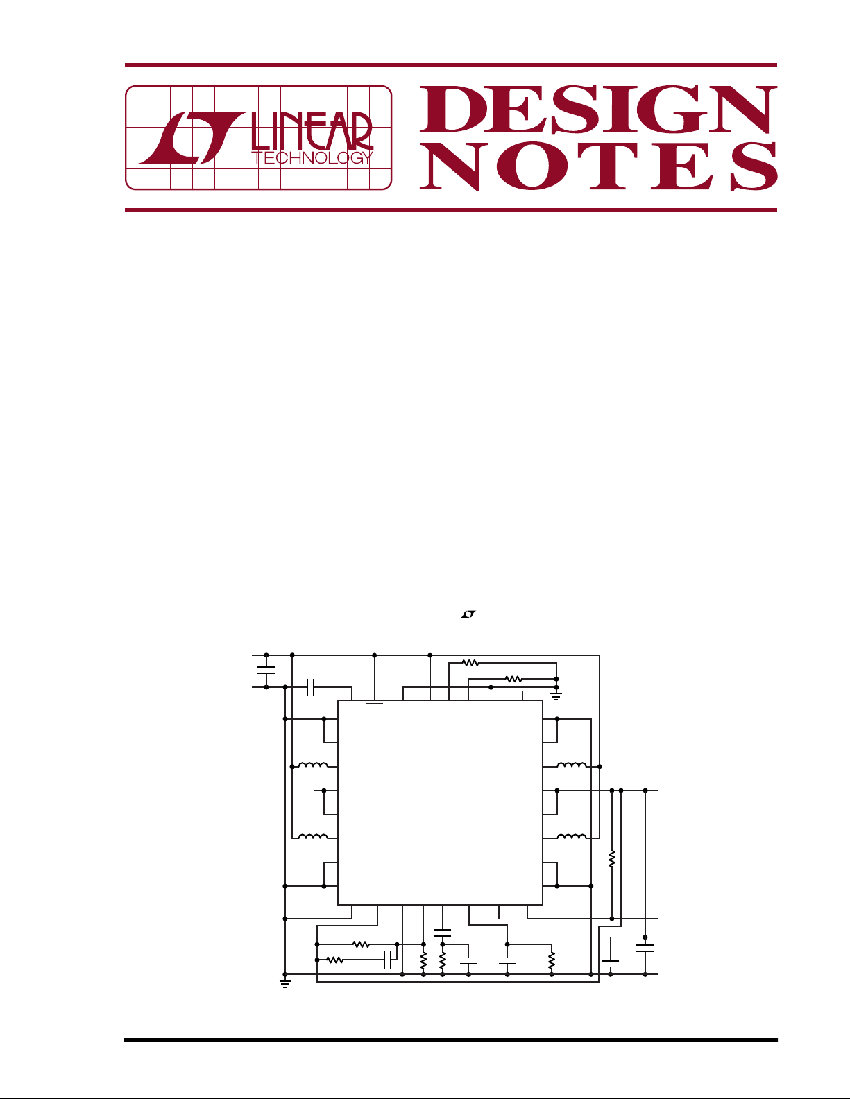
Figure 1. 2-Cell to 3.3V/2.5A Boost Converter
5A peak current capability and an effective switch R
DS(ON)
of 40mΩ (NMOS) and 50mΩ (PMOS), the LTC3425 is
capable of efficiently delivering 2.5A load current from a
0.8mm maximum profile, 32-pin 5mm × 5mm QFN
package.
Multiple Operating Modes Optimize Performance in
Different Applications
The LTC3425 can be configured for automatic Burst
®
operation, fixed frequency mode with forced
Mode
continuous conduction or fixed frequency mode with
pulse skipping. Programmable automatic Burst Mode
operation is ideal for portable applications, where the
load current can vary over a wide range and efficiency is
paramount. A quiescent current of just 12µA in Burst
, LTC, LT and Burst Mode are registered trademarks of Linear Technology
Corporation.
R
75k
LIM
COM SYNCOUT
GNDD
GNDD
V
V
GNDC
GNDC
C
C
P
15pF
0.022µF
25
SWD
OUTD
OUTC
SWC
B
24
23
L4
2.7µH
22
V
BULK
OUT
3.3V
2.5A
PGOOD
C
OUT
10µF
×4
GND
21
20
L3
2.7µH
19
18
17
R
27k
R1
100k
B
DN332 F01
C
47µF
C
330pF
C
R
15k
T
Z
03/04/332
Page 2
Mode operation extends battery life during light load
operation. For noise-sensitive applications fixed frequency
mode can be selected, with either forced conduction for
low noise at light load or pulse skipping for improved light
load efficiency. Quiescent current in shutdown is less
than 1µA.
Fault Protection
The LTC3425 includes short-circuit protection, programmable peak current limit and thermal shutdown.
High Power and High Efficiency in
a Small Package
Figure 1 shows an LTC3425 application using all ceramic
capacitors and low profile inductors to deliver 2.5A load
current at 3.3V from a 2-cell input (V
of 2V to 3V).
IN
Maximum component profile is only 2.5mm. In this
example, the oscillator frequency is programmed for
4MHz (1MHz/phase), resulting in 10mV
output ripple
P-P
at full load (see Figure 2). The burst resistor is selected to
automatically transition from Burst Mode operation to
fixed frequency mode when the load exceeds 100mA for
optimal efficiency (peaking at 96%) over the load range
(see Figure␣ 3). No-load input current is only 39µA at 2.4V.
The current mode architecture results in excellent transient
response during a load step (see Figure 4). The use of a
small feed-forward RC network across the top feedback
resistor provides improved transient response and reduced
output ripple in Burst Mode operation, especially when
using low output capacitor values. The feed-forward capacitor also compensates for the effect of stray capacitance at
the FB pin when using large value feedback resistors.
The open-drain PGOOD output goes low when V
11.5% below its regulated value and goes high when V
OUT
is
OUT
is within 9% of its regulated value.
Conclusion
The LTC3425’s multiphase architecture makes it possible
to deliver high power in a small, low profile package with
very low output ripple. It offers features that are demanded in high performance portable applications, including output disconnect, automatic Burst Mode and
high efficiency over a wide load range. It also offers
flexible design features, including its programmable softstart, current limit and oscillator frequency, external compensation and multiple available operating modes.
Figure 2. Output Voltage Ripple at 2.5A Load
for Converter of Figure 1
100
VIN = 3V
90
80
70
60
50
40
EFFICIENCY (%)
30
20
10
0
0.1
VIN = 2V
1 10 100 1k 10k
VIN = 2.4V
LOAD CURRENT (mA)
DN332 F03
Figure 3. Efficiency vs Load of the Converter in Figure 1
Data Sheet Download
http://www.linear.com/go/dnLT3425
V
OUT
100mV/DIV
AC COUPLED
I
LOAD
0.5A/DIV
0A
VIN = 2.4V 100µs/DIV DN332 F04
V
= 3.3V
OUT
= 0.5A TO 1.5A
I
LOAD
Figure 4. Response of the Circuit in Figure 1
to a 1A Load Step
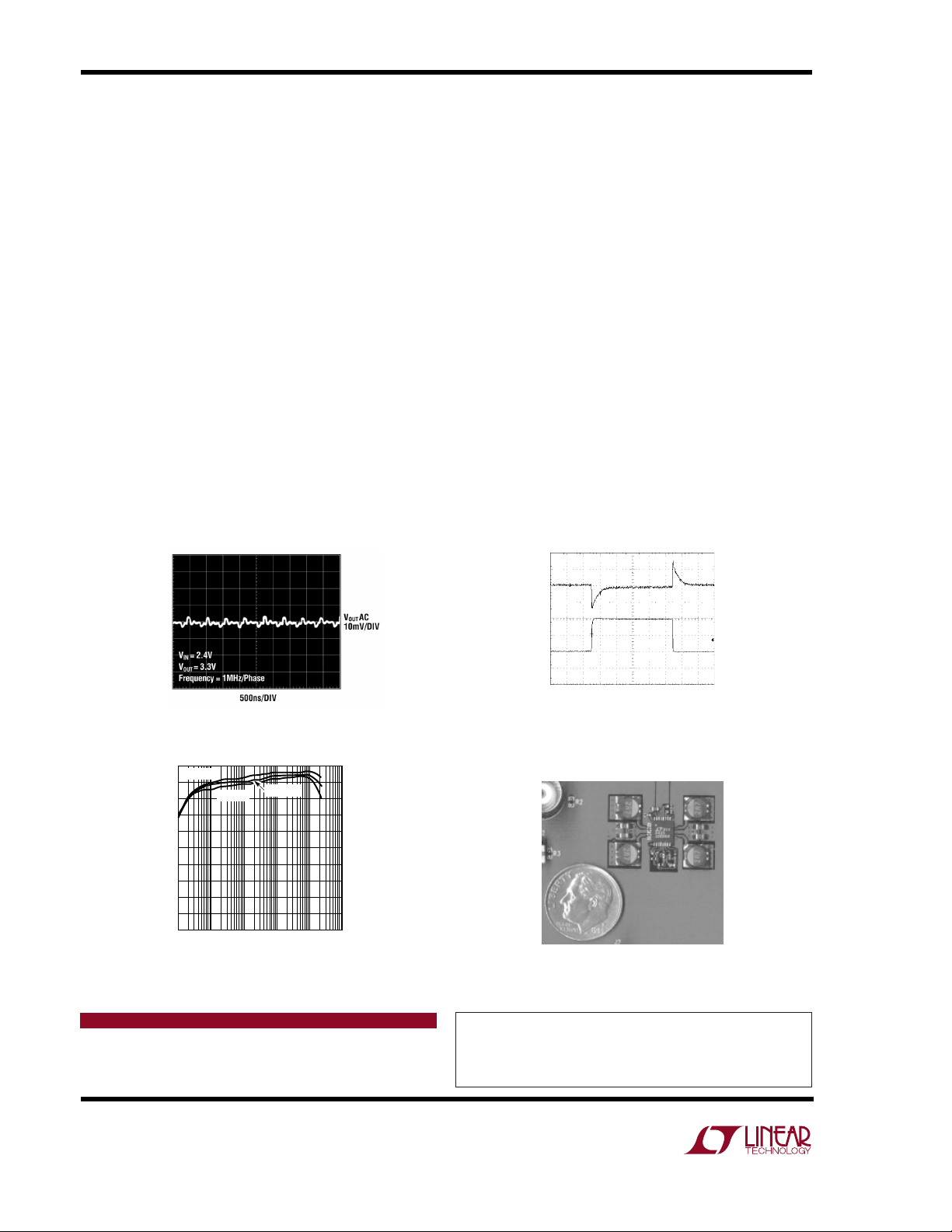
Figure 5. The LTC3425 Can Deliver 10W in a
Low Profile 0.7in2 Footprint
For applications help,
call (408) 432-1900, Ext. 2759
Linear Technology Corporation
1630 McCarthy Blvd., Milpitas, CA 95035-7417
(408) 432-1900 ● FAX: (408) 434-0507 ● www.linear.com
dn332f LT/TP 0304 344K • PRINTED IN THE USA
LINEAR TECHNOLOGY CORPORATION 2004
 Loading...