

advertisement
Cascadable 7A Point-of-Load Monolithic Buck Converter
Design Note 387
Peter Guan
Introduction
Easy-to-use and compact point-of-load power supplies
are necessary in systems with widely distributed, high
®
current, low voltage loads. The LTC
3415 provides a
compact, simple and versatile solution. It includes a pair
of integrated complementary power MOSFETs (32mΩ
top and 25mΩ bottom) and requires no external sense
resistor. A complete design requires an inductor and
input/output capacitors, and that’s it. The result is a fast,
constant frequency, 7A current mode DC/DC switching
regulator.
Features
The overall solution is extremely compact since the
LTC3415’s 5mm × 7mm QFN package footprint is small
and its high operating frequency of 1.5MHz allows the
use of small low-profi le surface mount inductors and
ceramic capacitors. For loads higher than 7A, multiple
LTC3415s can be cascaded to share the load while running mutually anti-phase, which reduces overall ripple
at both the input and the output.
Other features include:
• Spread spectrum operation to reduce system noise
• Output tracking for controlled V
ramp-up and
OUT
ramp-down
• Output margining for easy system stress testing
• Burst Mode® operation to lower quiescent current and
boost effi ciency during light loads
• Low shutdown current of less than 1µA
• 100% duty-cycle for low drop out operation
• Phase-lock-loop to allow frequency synchronization of
±50% of nominal frequency
• Internal or external ITH compensation for ease of use
or loop optimization, respectively
Operation
The LTC3415 offers several operating modes to optimize
effi ciency and noise reduction: Burst Mode operation,
pulse-skipping mode or forced continuous mode. The
mode is set by t ying the Mode pin to SV
, SVIN/2 or SGND,
IN
respectively. Burst Mode operation offers high effi ciency
at light load by shutting off the internal power MOSFETs
as well as most of the internal circuitry between pulses.
Forced continuous mode maintains a constant switching
frequency throughout the entire load range, making it
easier to fi lter switching noise for sensitive applications.
P u l s e - s k i p p i n g m o d e a l l o w s c o n s t a n t f r e q u e n c y o p e r a t i o n
until the inductor current reaches zero, at which point it
goes into discontinuous operation and fi nally it will skip
cycles. Pulse-skipping mode offers low output voltage
ripple while of fering effi ciency levels be tween Burst Mode
operation and forced continuous mode.
, LTC, LT and Burst Mode are registered trademarks of Linear Technology
Corporation. All other trademarks are the property of their respective owners.
0.1µF
V
IN
47µF
6.3V
3x
10pF
MODE SV
38 37 36 35 34 33 32
CLKOUT RUN PV
1
NC
2
SGNDSGND
3
PLLLPF
4
PV
IN
5
PV
IN
6
SW
7
SW
8
SW
9
SW
10
MODE
11
CLKIN
12
PHMODE
PGND PGND PGND PGND PGND PGND PGND
13 14 15 16 17 18 19
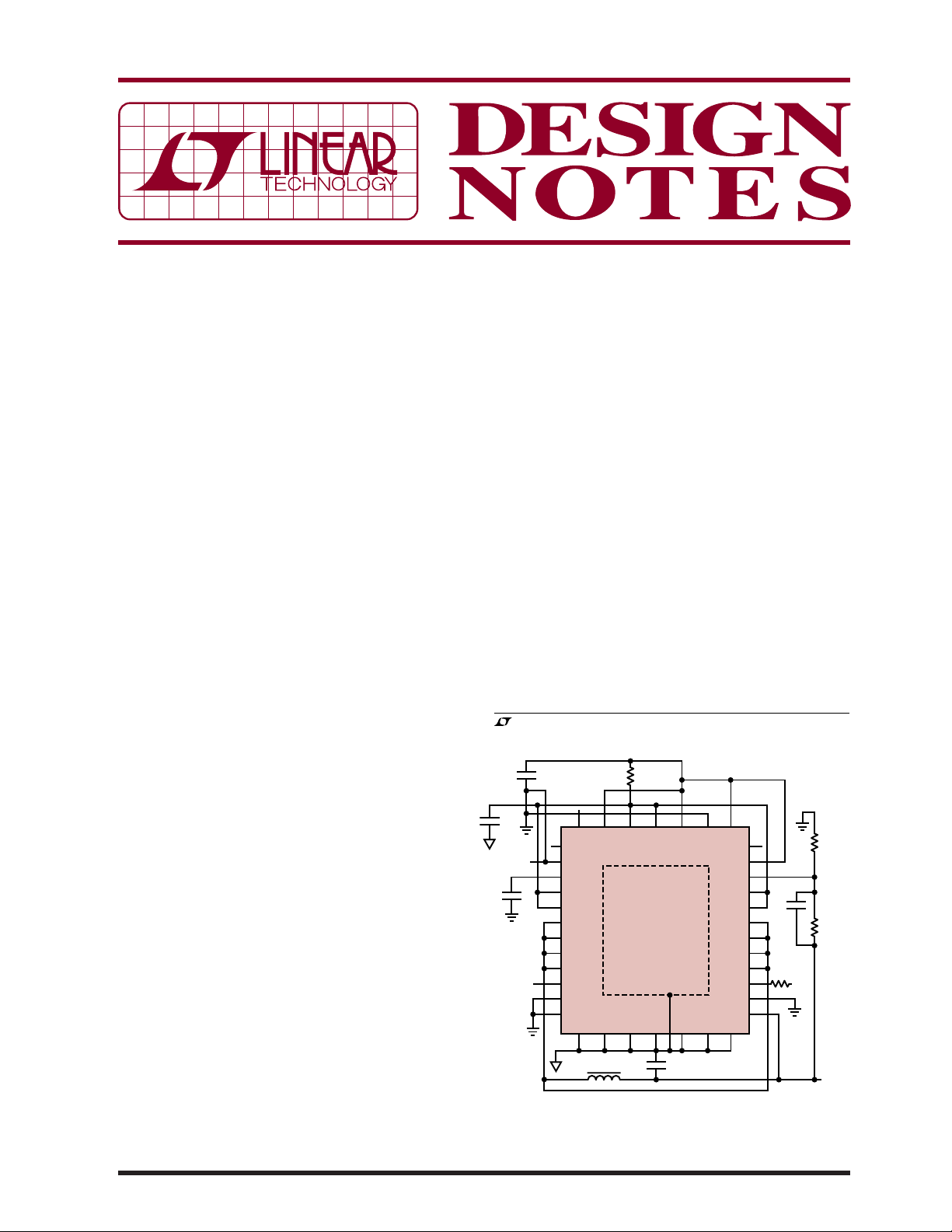
Figure 1. 3.3V to 1.8V/7A Application
1Ω
INPVINSVINITHMITH
LTC3415EUHF
5mm × 7mm QFN
0.2µH
PGND (39)
100µF, 6.3V
2x
31
NC
30
TRACK SV
29
V
FB
28
PV
IN
27
PV
IN
26
22pF
SW
25
SW
24
SW
23
SW
10k
22
PGOOD
21
BSEL
20
MGN
15k
DN387 F01
IN
30.5k
IN
V
OUT
1.8V/7A
04/06/387
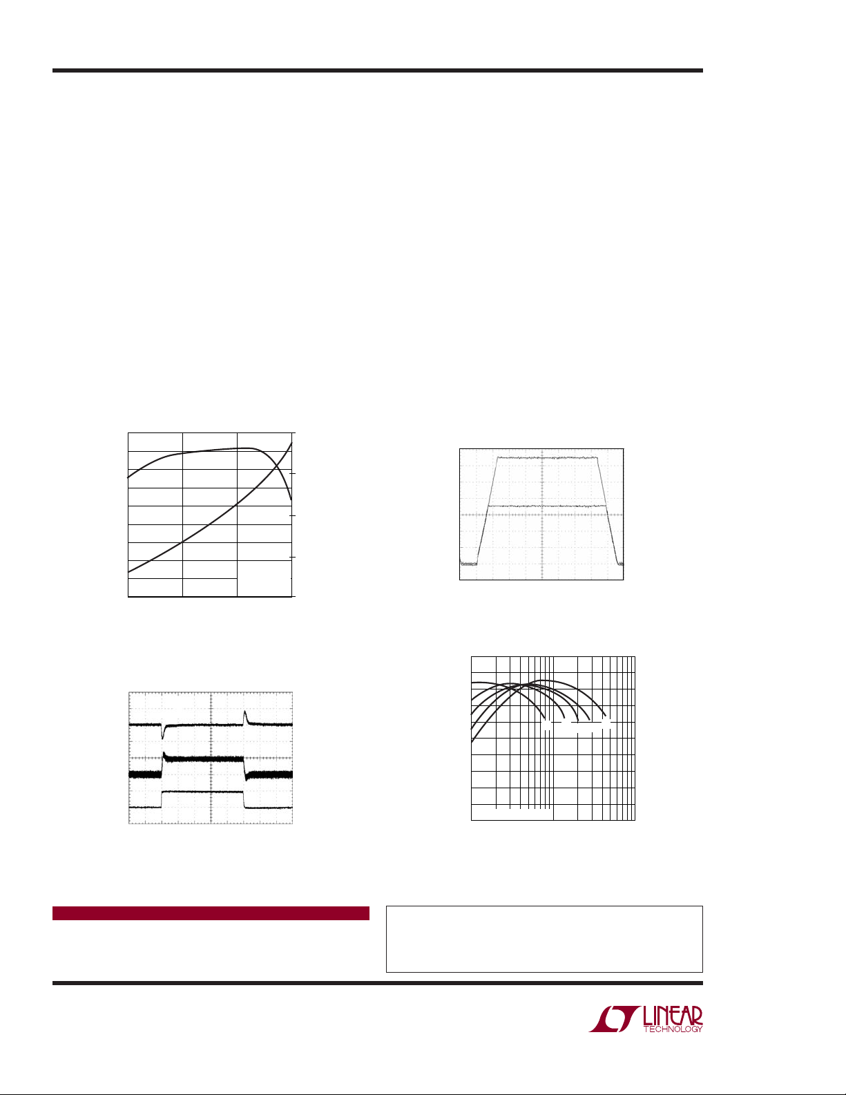
Figure 1 shows an application of the LTC3415 in a 3.3V
to 1.8V/7A step-down converter confi guration. Figure 2
shows its effi ciency and power loss vs load current in
Burst Mode operation. Ef fi ciency reaches as high as 92%.
Figure 3 shows its fast transient response to a 5A load
step. As shown, V
recovers in 10µs with a dip of less
OUT
than 100mV. Frequency can be changed easily from its
nominal 1.5MHz to 1MHz or 2MHz by simply strapping
the PLLLPF pin to SGND or SV
, respectively. Or if a
IN
particular frequency is desired, an external clock can
be used to synchronize the operating frequency from
750KHz to 2.25MHz with the internal phase-lock-loop.
Spread spectrum operation is available for EMI-sensitive
applications by tying the CLKIN pin to SV
.
IN
For applications that require controlled output voltage
tracking between various outputs in order to prevent
excessive current draw or even latch-up during turn-on
and turn-off, the LTC3415 has a Track pin that allows
the user to program how its output voltage ramps dur-
95
90
85
80
75
70
EFFICIENCY (%)
65
60
55
50
10
EFFICIENCY
POWER LOSS
VIN = 3.3V
V
OUT
BURST MODE
100 10000
LOAD CURRENT (mA)
1000
= 1.8V
DN387 F02
10000
1000
POWER LOSS (mW)
100
10
1
ing start-up and shutdown. Figure 4 shows the output
waveforms of two LTC3415s in track mode.
Greater than 7A Outputs
By stacking multiple LTC3415s together, more output
power is attained without increasing the number of input
and output capacitors. Operating multiple LTC3415s out
of phase not only allows accurate current sharing, but it
also reduces the overall voltage ripple at both the input
and the output, thus allowing fewer capacitors. Figure
5 shows an effi ciency curve of the LTC3415 in 1-phase,
2-phase, 3-phase, 4-phase and 6-phase operation.
Conclusion
With its many operational features and compact total
solution size, the LTC3415 is an ideal fi t for today’s pointof-load power supplies. It allows for accurate, compact,
effi cient and scalable power supplies with advanced
features, including tracking and margining.
=
V
OUT2
3.3V/7A
500mV/DIV
=
V
OUT1
1.8V/14A
500mV/DIV
500µs/DIV
Figure 4. Output Tracking of Two LTC3415s
DN387 F04
Figure 2. Effi ciency and Power Loss of
3.3V to 1.8V/7A Application in Figure 1
V
L = 0.2µH
C
Figure 3. V
= 3.3V
IN
= 2 × 100µF
OUT
OUT
40µs/DIV
Transient Response to a 0A to 5A
DN387 F03
Load Step of the Circuit Shown in Figure 1
Data Sheet Download
www.linear.com
Linear Technology Corporation
1630 McCarthy Blvd., Milpitas, CA 95035-7417
(408) 432-1900
●
FAX: (408) 434-0507 ● www.linear.com
= 1.8V
V
OUT
100mV/DIV
AC COUPLED
I
INDUCTOR
5A/DIV
STEP
I
OUT
0A TO 5A
5A/DIV
100
95
90
85
80
75
70
EFFICIENCY (%)
65
60
55
* PHASE OPERATION
50
1
1*
10 100
LOAD CURRENT (A)
6*
2*
4*
3*
DN387 G05
Figure 5. Effi ciency vs Load Current of
LTC3415s in Multiphase Operation
For applications help,
call (408) 432-1900, Ext. 2759
dn387f LT/TP 0406 305K • PRINTED IN THE USA
© LINEAR TECHNOLOGY CORPORATION 2006
 Loading...